Complementary Split Ring Resonator for Isolation Enhancement
in 5G Communication Antenna Array
Raghuraman Selvaraju1, Mohd H. Jamaluddin1, *, Muhamad R. Kamarudin2, Jamal Nasir3, and Muhammad H. Dahri1
Abstract—A square-shaped complementary split ring resonator (CSRR) filtering structure for isolation improvement is presented in this paper. The proposed research work investigates the design and development of a simple and compact CSRR structure. In order to verify the performance of the proposed filtering element and to improve the isolation among the closely placed antenna elements, arrays of configured CSRR structures are implemented between two antenna elements. An array of configured CSRR elements has been integrated with the printed antenna on the top and bottom layers. The proposed filtering elements offer an enhancement in isolation by 25 dB as compared to the simple array. The entire configuration has been simulated using the Ansoft HFSS simulator. Finally, the proposed design is fabricated and experimentally validated. In the experiment, coupling suppression of
−51 dB at the operating frequency is successfully achieved, resulting in a recovery of the array pattern. The proposed antenna is highly efficient, which is suitable to be utilized for 5G communication.
1. INTRODUCTION
In recent years, the intense growth of many advanced services increases the demand for high data transmission capacity and hence high data rate. A single antenna element has a broad radiation pattern and low directivity. The antenna directivity can be increased by increasing the radiator physical dimensions, but it is impractical. Alternatively, the electrical size of the antenna can be increased by assembling an array of similar elements to increase the antenna directivity [1]. A phased array antenna consists of precisely organized, finite sized radiating elements, which are fed by a suitable feed network. Especially printed antennas are the best candidates for the phased array elements because of their advantages in terms of low profile, light-weight, low cost, and easy fabrication [2]. The mutual coupling between the antenna elements affects the terminal impedance, radiation pattern and the gain of the adaptive array [3]. To avoid the terminal impedance mismatch, the mutual impedance should be completely reactive (Zij = 0) at resonant frequency [4].
The mutual coupling becomes very critical in arrays where coupling arises from two reasons; free space radiation and surface wave effects [5, 6]. Various techniques have been suggested to mitigate the coupling effects by several researchers. These include open-circuit voltage method [7–9], S -parameter method [10], full-wave method [11], element pattern method [12], perturbation method [13] and calibration method [14]. These mathematical methods yield precise results; however, the complexity increases with the array size and beam scanning. Moreover, these methods require several preliminary experimental results to perform the coupling compensation.
Received 10 January 2018, Accepted 24 March 2018, Scheduled 24 April 2018 * Corresponding author: Mohd Haizal Jamaluddin ([email protected]).
1Wireless Communication Center, Universiti Teknologi Malaysia, Johor, Malaysia. 2Centre for Electronic Warfare, Information and
Cyber, Cranfield Defence and Security, Cranfield University, Defence Academy of the United Kingdom, Shrivenham, SN6 8LA, UK.
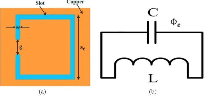
are well known single negative metamaterial elements. The first model of mu-negative (MNG) SRR was originally proposed by Pendry et al. [31]. The application of Babinet’s principle leads to the implementation of complementary SRR [32]. The epsilon negative (ENG) CSRR was first introduced in [33] and derived by applying duality to the SRR, replacing metal with dielectric and vice versa. The electrical and magnetic properties of the CSRR are interchanged with respect to the SRR. However, the resonant frequency of both the CSRR and the SRR should be approximately the same [33]. Therefore, in a straightforward way the resonance frequency of the CSRR can be derived from SRR. Figure 1 shows the schematic diagram and equivalent circuit model of CSRR. The major advantage of the CSRR is high filtering (band-rejection) capability which is useful for coupling suppression, compact size (less than one-tenth of a λ) and easy fabrication.
(a) (b)
Figure 1. CSRR unit cell. (a) Schematic diagram. (b) Equivalent circuit model.
Several CSRR structures have been proposed only to reduce the amount of mutual coupling between array elements. This paper focuses on developing a CSRR filtering element to make the mutual impedance purely reactive in antenna arrays (Zij = 0). This paper is organized as follows. Section 2 consists of theoretical analysis. CSRR computational modeling and verification are presented in Section 3. The filtering characteristics of the proposed CSRR are verified along with patch array antenna in Section 4 while the conclusion is made in Section 5.
2. THEORETICAL ANALYSIS
The SRR behaves as an externally driven LC resonant circuit. The resonance frequency of the SRR unit cell is determined by the self-inductance L and capacitance per unit length Cpul[31, 33–35].
The resonant frequency (f0) of the square SRR is given by
f0=
1
2π√LnetCnet (1)
whereLnetandCnetare the total inductance and capacitance of the structure. The net total capacitance
Cnet can be expressed as
Cnet= (cs+cg)
In Equation (2),csandcg are the series capacitance and gap capacitance, respectively. From the general capacitance equation, the gap capacitance cg is defined as
cg = ε0wt
g (3)
where w and t are the width and thickness of the metal rings, respectively, and ε0 is the free space permittivity.
The distributed capacitance cs is a function of the split gap dimension g and ring dimension ae, and is given as
cs= (4ae−g)cpul (4)
The capacitance per unit length (cpul) is calculated as
cpul=
√
εr
CZ0
(5)
Here εr is the effective permittivity of the medium, C the velocity of light, and Z0 the characteristic impedance of the line. Substituting the values of cs and cg in Equation (2), we get,
Cnet=
2ae− g 2
cpul+
ε0wt
g
(6)
The total inductance of the proposed circuit model can be calculated by using the following relation:
Lnet = (0.0002)l
2.303 log104l
w −γ
(7)
Here the parameterγ = 2.853 is a constant for the wire loop of square geometry, andlis the wire length which can be calculated as follows
l= 8ae−g (8)
The resonant frequency f0 can be calculated by substituting the total capacitance and inductance in Equation (1).
3. BAND GAP CHARACTERIZATION ANALYSIS
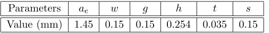
In order to design the proposed CSRR, first, a square-shaped SRR is designed, and it is converted into a complementary structure. The dimensions of the proposed CSRR are listed in Table 1. A standard 0.254 mm thickness Rogers RT Duroid material (ε = 2.2) is chosen as the substrate. The proposed CSRR is analysed by using the high frequency structural simulator (HFSS).
Table 1. Unit cell deimentions.
Parameters ae w g h t s
Value (mm) 1.45 0.15 0.15 0.254 0.035 0.15
To investigate the performance and find the stopband response of the CSRR, a pair of unit cells is loaded with the coplanar waveguide (CPW) as shown in Figures 2(a) and 2(b). The unit cells are arranged in a mirror orientation, and this mirror orientation does not significantly shift the operating frequency of the CSRR. The detailed study regarding this phenomenon is presented in [36]. The unit cell simulation setup (Figure 2(c)) shows that the CSRR structure is positioned at the middle of the waveguide. The front and back sides of a waveguide are defined as PEC walls, while its top and bottom sides are attributed as PMC walls, and the other two sides are used for the signal excitation.
(a) (b) (c)
Figure 2. Unit cell simulation setup. (a) Top view. (b) Bottom view. (c) Simulation setup.
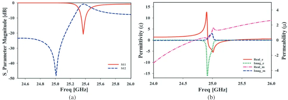
(a) (b)
Figure 3. Unit cell simulation response. (a)S-parameter. (b) Constitutive properties.
the scattering (S) parameters as given by the following equations [37, 38]. The calculated constitutive properties are plotted in Figure 3(b).
ε = n
z (9)
μ = n×z (10)
where the refractive index (n) and wave impedance (z) are calculated by using the following equations [37, 38].
n= 1
kdcos
−1
1−S112 +S212
2S21
(11)
Here kand dare the wave number and the distance between the ports, respectively.
z=
(1 +S11)2−S221
(1−S11)2−S221 (12)
The calculated constitutive parameters clearly show negative responses of permittivity that can be obtained by configured CSRR.
4. ISOLATION ENHANCEMENT USING CSRR
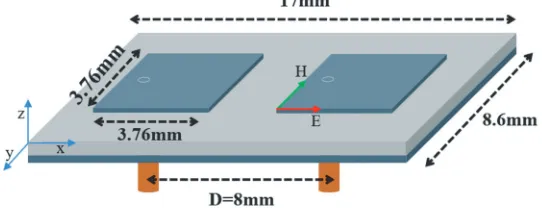
Figure 4. Printed patch array.
in Figure 4. The dimensions of the antenna element are calculated for an operating frequency of 25 GHz. The antennas are etched on the top of the standard Rogers RT Duroid substrate, and they are separated by a center-to-center distance of 8 mm (0.67λ). The total dimensions of the antenna array are 8.6×17 mm2.
In this proposed work, the antenna elements are arrayed in the electric plane. In antenna arrays at some distance, the total fields radiated by the array can be found by the sum of the fields radiated by individual elements of the array.
Array pattern= (Element pattern)×(Array f actor) (13) The array factor of a uniformly spaced two-element linear array is given by
Array f actor=
W1ej(
1
2)Ψ+W2e−j(
1 2)Ψ
(14)
whereWn are the complex weights (excitation coefficients) and
Ψ = πd
λ sinθ (15)
Here θrepresents the antenna radiation angle.
The effect of mutual coupling is not considered in the above formulation and is derived under ideal condition. Moreover, it is assumed that the elements of the array do not interact with each other and that the individual element radiation pattern (active element pattern) is same as the isolated element pattern. Obviously, such an assumption is erroneous in practical array antennas. Because when two antenna elements are closely placed, the current distribution on one is affected by the field radiated from the other. Due to this effect, the port impedance (active impedance) of all the array elements get modified thus severely affecting the array performance.
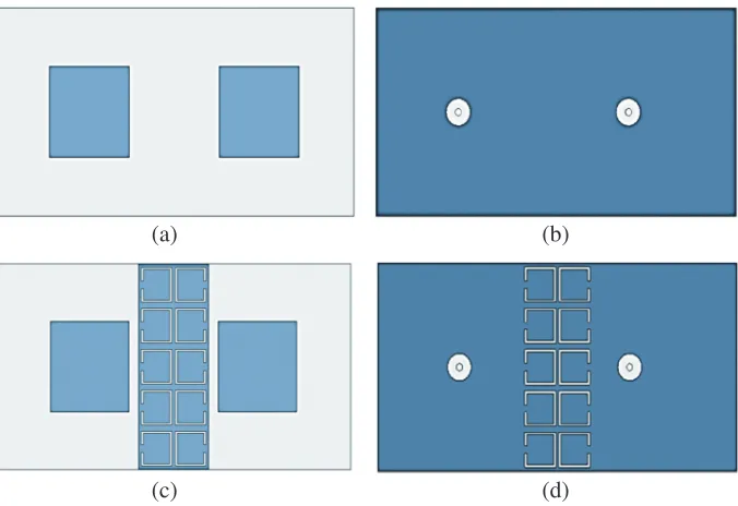
The solution to this problem is to bring the antenna mutual impedance (both real and imaginary parts) close to zero at antenna resonance. This condition can be achieved by increasing the isolation between the antenna elements. To improve the antenna isolation, the CSRR filtering structure is introduced between the microstrip patches. By placing single CSRR it is difficult to achieve such a good stopband response with conventional microstrip antenna. Here our concern is to enhance good band-rejection characteristics by arranging the CSRRs periodically in an array as illustrated in Figures 5(c) & 5(d). The CSRR filtering structures are introduced between the patches on surface and ground plan to investigate the mutual coupling suppression attributes.
5. SIMULATION VERIFICATION
(a) (b)
(c) (d)
Figure 5. Top and bottom view of two elements array with and without decoupling elements. (a) Top view without CSRR. (b) Bottom view without CSRR. (c) [Top view with CSRR. (d) Bottom view with CSRR.
Figure 6. Computed scattering parameter results of the two-element antenna array with and without CSRR.
(a) (b)
Figure 8. Computed mutual impedance with and without CSRR.
Figure 9. Normalized array radiation pattern at 25 GHz.
surface current distributions between the antenna elements with and without CSRR filtering elements are shown in Figure 7. It clearly shows that the current flow between the antenna elements is controlled by implementing the CSRRs.
The simulated mutual impedances (Z12) between array elements with and without filtering elements are shown in Figure 8. It is noticed that after implementing the CSRR the mutual impedance is close to zero. Furthermore, the ideal array pattern (without mutual coupling) is obtained by solving the above-mentioned array factor Equations (14) and (15) using MATLAB. The simulated mutual coupling suppressed and non-suppressed array patterns are compared with the ideal pattern. Figure 9 shows that compared to the simple array (without CSRR) pattern the mutual coupling suppressed array antenna pattern is closer to the ideal pattern.
Table 2 summarizes the simulated values (mutual coupling, maximum gain and radiation efficiency) of the proposed design and the simple array. After implementing the CSRR’s in between the array elements, the mutual coupling and nulls depth are considerably improved, and a slight improvement is also obtained in the array antenna gain, directivity and radiation efficiency.
Table 2. Array performance with and without CSRR.
At 25 GHz Without CSRR With CSRR
Return loss −31.4 dB −38.44 dB Mutual coupling −24.3 dB −53 dB
Maximum gain 10.39 dB 10.53 dB
Radiation efficiency 85% 88.5%
Peak directivity 11.39 11.53
Nulls depth −20 dB −55 dB
6. PRACTICAL IMPLEMENTATION
(a) (b)
(c) (d)
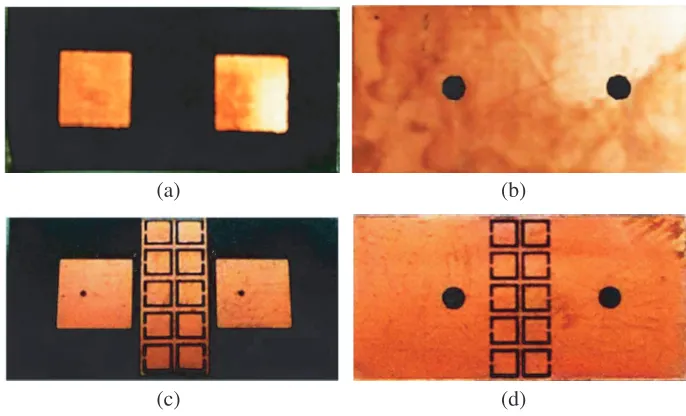
Figure 10. Prototype of the fabricated antenna array. (a) Top view without CSRR. (b) Bottom view without CSRR. (c) Top view with CSRR. (d) Bottom view with CSRR.
(a) (b)
Figure 11. Antenna measurement setup. (a) Scattering parameter measurement setup. (b) Radiation pattern measurement setup.
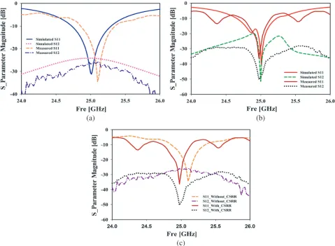
Figure 12 shows the simulated and measured S parameters results of the proposed design. The measuredS11 of the array is deviated a little from the simulated one. Also, measuredS12is better than the simulated one; however, at the required frequency it is very close to the simulated one. The slight deviation in the measured results is attributed to fabrication tolerance and the effect of measurement setup. Figure 13 shows the measured and computed normalized radiation patterns of the proposed array in the yz plane, with and without the CSRR elements. The main beam is pointing in the broadside direction with two nulls at±50. The simulated and measured radiation patterns are in close agreement with some deviations that has been explained previously.
(a) (b)
(c)
Figure 12. Computed and measured S-parameter results comparison. (a) Computed and measured results of an array without CSRR. (b) Computed and measured results of an array with CSRR. (c) Measured results of an array with and without CSRR.
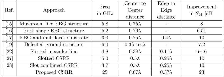
[15] Mushroom like EBG structure 5.8 0.75λ - 8
[16] Fork shape EBG structure 5.2 0.76λ - 6.51
[17] EBG and multilayer substrate 3.0 0.75λ 0.4λ 10
[19] Defected ground structure 6.0 0.3λto λ - 7.2
[22] Slotted meander line 4.8 0.38λ 0.11λ 6–16
[27] Slotted CSRR 5.0 0.5λ 0.25λ 10
[28] Slot combined CSRR 3.7 0.5λ 0.25λ 10
Proposed CSRR 25 0.67λ 0.37λ 23
7. CONCLUSIONS
In this work, a simple epsilon negative (ENG) CSRR band gap decoupling structure is investigated, and simulation and experiments are performed. From the experimental results, −51 dB isolation has been achieved at the operating frequency by implementing the proposed design. The improvement in isolation results in a recovery of the array pattern, which is evident from the pattern measurement performed. The computed and measured results conclude that employing the CSRR’s in between the radiators offers an excellent coupling reduction. The advantage of the proposed design is its small size (equal to λ/10) and ease of fabrication compared to other metamaterial structures. This isolation enhancement band gap structure can be used in various compact antenna arrays. In future, this work can be continued to analyze the performance of CSRR along with numerous array elements in a linear and a planar array configurations for different element spacings to obtain compact and accurate beam steering array.
ACKNOWLEDGMENT
This project is sponsored by the Ministry of Education Malaysia and Universiti Teknologi Malaysia under Vot 4J211, Vot 03G33, Vot 4J220, Vot 13H26 and Vot 11H59. The authors would like to thank the staff of the Wireless Communication Centre (WCC) of Universiti Teknologi Malaysia (UTM) for the technical support.
REFERENCES
1. Balanis, C. A., Antenna Theory: Analysis and Design, 3rd Edition, John Wiley & Sons, 2016. 2. Hansen, R. C., Microwave Scanning Antennas, R. C. Hansen (ed.), Vol. 1, Academic Press,
Apertures, 1964.
3. Gupta, I. and A. Ksienski, “Effect of mutual coupling on the performance of adaptive arrays,”
IEEE Transactions on Antennas and Propagation, Vol. 31, No. 5, 785–791, 1983.
4. Bait-Suwailam, M. M., M. S. Boybay, and O. M. Ramahi, “Electromagnetic coupling reduction in high-profile monopole antennas using single-negative magnetic metamaterials for MIMO applications,” IEEE Transactions on Antennas and Propagation, Vol. 58, No. 9, 2894–2902, 2010. 5. Pozar, D., “Input impedance and mutual coupling of rectangular microstrip antennas,” IEEE
Transactions on Antennas and Propagation, Vol. 30, No. 6, 1191–1196, 1982.
7. Su, T. and H. Ling, “On modeling mutual coupling in antenna arrays using the coupling matrix,”
Microwave and Optical Technology Letters, Vol. 28, No. 4, 231–237, 2001.
8. Huang, Z., C. A. Balanis, and C. R. Birtcher, “Mutual coupling compensation in UCAs: Simulations and experiment,” IEEE Transactions on Antennas and Propagation, Vol. 54, No. 11, 3082–3086, 2006.
9. Nasir, J., M. H. Jamaluddin, M. R. Kamarudin, Y.-C. Lo, R. Selvaraju, et al., “A four-element linear dielectric resonator antenna array for beamforming applications with compensation of mutual coupling,”IEEE Access, Vol. 4, 6427–6437, 2016.
10. Segovia-Vargas, D., R. Martin-Cuerdo, and M. Sierra-Perez, “Mutual coupling effects correction in microstrip arrays for Direction-Of-Arrival (DOA) estimation,” IEE Proceedings — Microwaves, Antennas and Propagation, Vol. 149, No. 2, 113–118, 2002.
11. Pasala, K. M. and E. M. Friel, “Mutual coupling effects and their reduction in wideband direction of arrival estimation,” IEEE Transactions on Aerospace and Electronic Systems, Vol. 30, No. 4, 1116–1122, 1994.
12. Steyskal, H. and J. S. Herd, “Mutual coupling compensation in small array antennas,” IEEE Transactions on Antennas and Propagation, Vol. 38, No. 12, 1971–1975, 1990.
13. Jamaluddin, M. H., R. Gillard, R. Sauleau, and M.-A. Milon, “Perturbation technique to analyze mutual coupling in reflectarrays,”IEEE Antennas and Wireless Propagation Letters, Vol. 8, 697– 700, 2009.
14. Huang, Q., H. Zhou, J. Bao, and X. Shi, “Calibration of mutual coupling effect for adaptive arrays composed of circularly polarized microstrip antennas,” Electromagnetics, Vol. 34, No. 5, 392–401, 2014.
15. Yang, F. and Y. Rahmat-Samii, “Microstrip antennas integrated with Electromagnetic Band-Gap (EBG) structures: A low mutual coupling design for array applications,” IEEE Transactions on Antennas and Propagation, Vol. 51, No. 10, 2936–2946, 2003.
16. Yang, L., M. Fan, F. Chen, J. She, and Z. Feng, “A novel compact Electromagnetic-Bandgap (EBG) structure and its applications for microwave circuits,” IEEE Transactions on Microwave Theory and Techniques, Vol. 53, No. 1, 183–190, 2005.
17. Rajo-Iglesias, E., O. Quevedo-Teruel, and L. Inclan-Sanchez, “Mutual coupling reduction in patch antenna arrays by using a planar EBG structure and a multilayer dielectric substrate,” IEEE Transactions on Antennas and Propagation, Vol. 56, No. 6, 1648–1655, 2008.
18. Islam, M. T. and M. S. Alam, “Compact EBG structure for alleviating mutual coupling between patch antenna array elements,” Progress In Electromagnetics Research, Vol. 137, 425–438, 2013. 19. Xiao, S., M.-C. Tang, Y.-Y. Bai, S. Gao, and B.-Z.Wang, “Mutual coupling suppression in
microstrip array using defected ground structure,” IET Microwaves, Antennas & Propagation, Vol. 5, No. 12, 1488–1494, 2011.
20. Wei, K., J. Li, L. Wang, Z. Xing, and R. Xu, “S-shaped periodic defected ground structures to reduce microstrip antenna array mutual coupling,”Electronics Letters, Vol. 52, No. 15, 1288–1290, 2016.
21. Khandelwal, M. K., B. K. Kanaujia, and S. Kumar, “Defected ground structure: Fundamentals, analysis, and applications in modern wireless trends,” International Journal of Antennas and Propagation, Vol. 2017, 2017.
22. Alsath, M. G. N., M. Kanagasabai, and B. Balasubramanian, “Implementation of slotted meanderline resonators for isolation enhancement in microstrip patch antenna arrays,” IEEE Antennas and Wireless Propagation Letters, Vol. 12, 15–18, 2013.
23. Sievenpiper, D., L. Zhang, R. F. Broas, N. G. Alexopolous, and E. Yablonovitch, “High-impedance electromagnetic surfaces with a forbidden frequency band,” IEEE Transactions on Microwave Theory and Techniques, Vol. 47, No. 11, 2059–2074, 1999.
27. Bait-Suwailam, M. M., O. F. Siddiqui, and O. M. Ramahi, “Mutual coupling reduction between microstrip patch antennas using slotted-complementary split-ring resonators,”IEEE Antennas and Wireless Propagation Letters, Vol. 9, 876–878, 2010.
28. Qamar, Z., L. Riaz, M. Chongcheawchamnan, S. A. Khan, and M. F. Shafique, “Slot combined complementary split ring resonators for mutual coupling suppression in microstrip phased arrays,”
IET Microwaves, Antennas &Propagation, Vol. 8, No. 15, 1261–1267, 2014.
29. Shafique, M. F., Z. Qamar, L. Riaz, R. Saleem, and S. A. Khan, “Coupling suppression in densely packed microstrip arrays using metamaterial structure,”Microwave and Optical Technology Letters, Vol. 57, No. 3, 759–763, 2015.
30. Capolino, F.,Theory and Phenomena of Metamaterials, CRC press, 2009.
31. Pendry, J. B., A. J. Holden, D. Robbins, and W. Stewart, “Magnetism from conductors and enhanced nonlinear phenomena,” IEEE Transactions on Microwave Theory and Techniques, Vol. 47, No. 11, 2075–2084, 1999.
32. Hsue, C.-W., Y.-W. Chang, and S.-L. Jang, “Comments on babinet’s principle,” Forum for Electromagnetic Research Methods and Application Tecchnologies (FERMAT), Vol. 16, No. 3, Jul.– Aug. 2016.
33. Falcone, F., T. Lopetegi, J. D. Baena, R. Marqu´es, F. Mart´ın, and M. Sorolla, “Effective negative-/spl epsiv/stopband microstrip lines based on complementary split ring resonators,”IEEE Microwave and Wireless Components Letters, Vol. 14, No. 6, 280–282, 2004.
34. Vendik, I., O. Vendik, and M. Odit, Theory and Phenomena of Metamaterials, Metamaterial Handbook, F. Cappolino (ed.), 2009.
35. Bahl, I. J. and P. Bhartia, Microwave Solid State Circuit Design, John Wiley & Sons, 2003. 36. Penciu, R., K. Aydin, M. Kafesaki, T. Koschny, E. Ozbay, E. Economou, and C. Soukoulis,
“Multigap individual and coupled split-ring resonator structures,”Optics Express, Vol. 16, No. 22, 18 131–18 144, 2008.
37. Smith, D., D. Vier, T. Koschny, and C. Soukoulis, “Electromagnetic parameter retrieval from inhomogeneous metamaterials,” Physical Review E, Vol. 71, No. 3, 036617, 2005.