Circuit Design Challenges for Nanoscale
CMOS based Devices
V. Srikar Kumar1, Cheng Xin2
Assistant Professor, Dept. of ECE, Osmania University, Hyderabad, Telangana, India1
PhD, Dept. of ECE, University of Toronto, Toronto, Canada2
ABSTRACT:In recent years, subthreshold operation has gained a lot of attention due to ultra-low-power consumption in nanoscale based applications requiring low to medium performance. It has also been shown that by optimizing the device structure, power consumption of digital subthreshold logic can be further minimized while improving its performance. Therefore, subthreshold circuit design is very promising for future ultra-low-energy sensor applications as well as high-performance parallel processing. This paper deals with various device and circuit design challenges associated with the state of the art in optimal digital subthreshold circuit design and reviews device design methodologies and circuit topologies for optimal digital subthreshold operation. This paper identifies the suitable candidates for subthreshold operation at device and circuit levels for optimal subthreshold circuit design and provides an effective roadmap for digital designers interested to work with nanoscale applications.
I.INTRODUCTION
II. APPLICATION AREAS
Subthreshold digital circuits will be suitable only for specific applications which do not need high performance, but require extremely low power consumptions. This type of applications include medical equipments [2-4] such as sensors [5-7], nanowire detectors[8], aptamers [9], hearing aids and pace- maker [10, 11], and self-powered devices [1]. Subthreshold circuits can also be applied to applications with bursty characteristics in which the circuits remain idle for an extended period of time. The original active time period in strong inversion region is being extended throughout the idle time period running in subthreshold region. The same number of operations is performed in both cases, but with much lower power consumption in the subthreshold operation.
III. CHALLENING ISSUES IN SUB-THRESHOLD DESIGN
Various device and circuit challenges have been identified which need to be addressed for the advancement of the subthreshold design. This section provides an interesting insight and challenges for designers interested to work with energy-constrained applications, particularly taking advantage of subthreshold circuits.
Exploring Logic Families Optimal for Subthreshold Circuit Design.
The low Vdd results in a reduced ION/IOFF ratio that can reduce robustness. Static CMOS gates continue to function in subthreshold, but because of enhanced problem of short-channel effects due to variations at nano scale [7], logic families other than CMOSmay offer greater resiliency to certain variation sources such as voltage or process. Therefore, design of robust subthreshold logic circuits exploring logic families other than static CMOS is another open area for exploration [12].
Developing industrial subthreshold benchmark circuits
Since there are no industrial subthreshold devices to compare the results with those of any optimized subthreshold devices [1], there is a need to build benchmark circuits with the subthreshold devices to compare issues such as variation immunity, power, and performance with respect to constructed subthreshold circuits with standard devices.
Advancement in CAD Tools
Another significant issue for subthreshold operation is system verification. Using SPICE for verifying large systems rapidly becomes infeasible when the number of process corners, temperature corners, and voltage supply values increases. Hspice is too slow to run larger circuits and Nanosim can simulate large netlists in reasonable time, but will not correctly model the devices for supply voltages below 1V. Therefore, need for either modifications of current simulators or a new subthreshold circuit simulator to verify large systems running at such ultra-low voltages and to estimate the power dissipation of circuits. Advances in CAD tools to account for this problem become necessary. These tools must also address statistical distributions of delay and power introduced by local variations
Architectures for Optimal Subthreshold Circuits
There is much future work opportunities in the area of architectures for subthreshold circuits. One area is the use of pipelining and massively parallel architectures that increase the activity factor of a circuit and requires minimum supply voltage operation. There is also great need for developing complete subthreshold standard cell library which will provide further opportunities to optimize for minimal energy dissipation.
V. DEVICE-LEVEL OPTIMIZATION METHODOLOGIES FOR SUB-THRESHOLD OPERATION
Standard transistors can be operated in the subthreshold region to implement subthreshold logic. Standard transistors are called “super-threshold transistors” that are design for ultrahigh-performance. After investigation, it has been concluded that standard transistors are not suitable for subthreshold operation. Hence some device optimization methodologies have been suggested, for subthreshold operation.
CMOS Technology for Subthreshold Operation
CMOS technology can be modified in the following ways for subthreshold operation.
1) Changing Channel Doping Profile for Subthreshold Operation
In bulk CMOS design halo and retrograde doping are used to suppress the short-channel effects. The main functions of halo doping and retrograde wells are to reduce drain-induced barrier lowering (DIBL), prevent body punch through, and control the threshold voltage of the device independent of its subthreshold slope. However, in subthreshold operation, the overall supply bias is small (in the order of 0.15V–0.3V).Consequently, the effects of DIBL and body punch through are also negligible.
Hence, we need not include this doping regions in our device. This results in the following conclusions:
A simplified process technology in terms of process steps and cost.
A reduction in the junction capacitances.
Reduction in the capacitance of the bottom junction.
Reduction in substrate noise effects and parasitic latch-up.
2) Oxide Thickness Optimization for Subthreshold Operation
In regular CMOS a minimum Tox is used for good subthreshold slope. However, minimum possible oxide thickness may not be suitable for subthreshold operation because it does not result in minimum energy consumption.
In the subthreshold operation, intrinsic gate capacitance is dominated by depletion capacitance but the parasitic capacitances like overlap and fringe capacitances will eventually dominate if the oxide is too thin. In the subthreshold operation, the effective gate capacitance Cg of a transistor is dominated by the intrinsic depletion and the parasitic (both overlap and fringe) capacitances that strongly depend on Tox. So oxide thickness should be optimized considering both the transistor effective capacitance and the subthreshold slope to achieve lowest power consumption.
3) Utilizing Reverse Short-Channel Effects for Subthreshold Operation
The side effects that appear in regular MCOS can be used for our benefit in subthreshold operation. The RSCE are used to improve drive current, capacitance, process variation, subthreshold swing, and improved energy/dissipation.
SCE (or Vth roll-off) is a phenomenon in short-channel devices where Vth decreases as the channel length is reduced. Non-uniform HALO [9] doping is used to reduce this problem by making the depletion widths narrow and hence reducing the DIBL effect. As a byproduct of HALO, a short channel device shows RSCE behavior where the Vth decreases as the channel length is increased. In subthreshold circuits, the SCE mechanism is not as strong as in super-threshold circuits because the drain-to-source voltage is very small. On the other hand, RSCE is still significant enough to affect the subthreshold performance. Moreover, current becomes an exponential function of Vth in subthreshold region, which makes it possible to use longer channel-length devices that utilize RSCE for improving drive current.
4) New Device Sizing Based on Subthreshold Logical Effort
For regular CMOS, the optimal ratio of PMOS width (Wp) to NMOS width (Wn) for achieving equivalent current drivability is approximately 2.5:1 due to the mobility difference between the carriers between the PMOS and NMOS devices. But for subthreshold operation this ratio reduces to 1.5:1 which gives equal delays for the rise and fall transitions at Vdd = 0.2V. This is because the drive-current in subthreshold designs is an exponential function of the terminal voltages
DGSOI Technology with Co-design Methodology for Optimal Subthreshold Operation
(DGMOS) transistors have near ideal subthreshold slope and negligible junction capacitance which makes them suitable for subthreshold operation. The thin and fully depleted silicon body between the two gates, have an excellent gate control over the channel.
Also the un-doped thin silicon body provides negligible source/drain p-n junction capacitance, which greatly improves the circuit performance. It can be noted that due to near ideal subthreshold slope, the DG-SOI devices have higher ON-current compared to the bulk devices. DG-SOI inverter has almost one order of magnitude lower PDP than the corresponding bulk device. This is due to the fact that the intrinsic capacitance of DG-SOI is negligibly small and hence the switching energy is extremely low.
Carbon Nanotube (CNFETs) Technology for Subthreshold Operation
Carbon nano tubes (CNTs) and molecular transistors are a very attractive alternative to nanoscale transistors[13]. CNTs are sheets of graphite rolled in the shape of a tube. Absence of scattering in the channel is the characteristic of ballistic devices which make them ultrahigh speed and apt for high-performance circuit design.
V. LOGIC FAMILIES FOR SUB-THRESHOLD OPERATION
In this section, we will present the scope of various logic families other than static CMOS for designing optimal subthreshold logic circuits. The following logic families are suitable for designing more robust and energy efficient subthreshold circuits with some tradeoff.
Subthreshold CMOS Logic
Sub-threshold CMOS (Sub-CMOS) logic [14, 15] is the regular CMOS logic operated in the subthreshold region. The voltage transfer characteristics (VTC) of the inverter gate running in subthreshold mode is closer to ideal compared to the VTC in normal strong inversion region. The improvement is due to
Increase in the circuit gain, gm.
Better noise margins.
More freedom in sizing.
Sensitivity to Power Supply Variation with decreasing power supply value for subthreshold CMOS.
Subthreshold Pseudo-NMOS Logic
In subthreshold region, Pseudo-NMOS logic is more robust than Pseudo- NMOS logic in strong-inversion,
voltage levels swing rail-to-rail due to large gain in subthreshold region
does not suffer from low logic level degradation problem
Operates faster than CMOS[8] consuming less area.
Two main disadvantages of Pseudo-NMOS in strong inversion compared to CMOS are higher power consumption and less robustness, which are eliminated in subthreshold region due to ideal device characteristics. In summary, Pseudo nMOS for subthreshold has better PDP and comparable robustness to static CMOS.
VT Sub-CMOS Logic
Fig. 1. VT-Sub-CMOS logic
This figure has been taken from the paper titled “Robust subthreshold logic for ultra-low power operation” written by Soeleman, H.; Roy, K. and Paul, B.C.
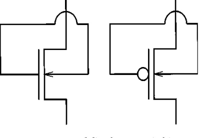
Sub-DTMOS logic
Sub-DTMOS logic provides an alternative way to achieve the same stability with direct substrate biasing without using additional control circuitry as in the case of VT-sub-CMOS logic. Sub-DTMOS logic uses transistors whose gates are tied to their substrates (Fig. 2). As the substrate voltage in sub-DTMOS logic changes with the gate input voltage, the threshold voltage is dynamically changed.
Fig. 2. DT-NMOS (left) and DT-PMOS (right)
This figure has been taken from the paper titled “Robust subthreshold logic for ultra-low power operation” written by Soeleman, H.; Roy, K. and Paul, B.C.
causes a lower effective normal field. The reduced threshold voltage, lower normal effective electric field, and higher mobility results in higher on-current drive in DTMOS [16] than that of a regular MOS transistor.
VI.NEARTHRESHOLDCOMPUTING
Near-threshold computing (NTC) can be considered as future work for sub-threshold computing. As we all know Moore’s law has failed to ensure proportionate increases in performance or energy efficiency with decreasing feature size and integration capacity. From the 65 nm technology, device scaling no longer delivers the energy gains that supported the semiconductor industry. The supply voltage and dynamic energy efficiency improvements have stagnated, while leakage currents continue to increase. Heat removal limits have been placing a further restriction. The near-threshold strategy provides 10X or higher energy efficiency improvements at constant performance through widespread application of near-threshold computing (NTC), where devices are operated at or near their threshold voltage Vth. This a relatively new technology and there is a lot of ongoing research in this field.
VII.CONCLUSION
As supply voltage continues to scale with each new generation of CMOS technology, Sub-threshold design is an inevitable choice in the semi-conductor road map for achieving ultra-low power consumption. Device optimization is a must for optimal subthreshold operation to further reduce power and enhance performance. Comparative studies shows that double gate SOI devices and CNFETs are better candidates to work for subthreshold operation than Bulk CMOS devices. At circuit level, Sub-Pseudo-NMOS, Sub-DTPT and Sub-domino logics can be considered for robust subthreshold operation due to their improved performance and better stability for PVT variations with reduced or comparable energy/switching to that of conventional static CMOS logic. Device/Circuit Codesign methodology can further enhance subthreshold operation in terms of performance and robustness.
REFERENCES
[1] B. H. Calhoun and A. Chandrakasan, "Characterizing and modeling minimum energy operation for subthreshold circuits," presented at the Proceedings of the 2004 international symposium on Low power electronics and design, Newport Beach, California, USA, 2004.
[2] S. Farid, X. Meshik, M. Choi, S. Mukherjee, Y. Lan, D. Parikh, et al., "Detection of Interferon gamma using graphene and aptamer based FET-like electrochemical biosensor," Biosensors and Bioelectronics, vol. 71, pp. 294-299, 2015.
[3] Souvik Mukherjee, Xenia Meshik, Min Choi, Sidra Farid,, Debopam Datta, Yi Lan, Shripriya Poduri, Ketaki Sarkar, Undarmaa Baterdene, Ching-En Huang,, Yung Yu Wang, Peter Burke, Mitra Dutta, Michael A. Stroscio, "A Graphene and Aptamer Based Liquid Gated FET-Like Electrochemical Biosensor to Detect Adenosine Triphosphate," IEEE Transactions on NanoBioscience, vol. 14, pp. 967 - 972, 2015.
[4] K. Xu, M. Purahmad, K. Brenneman, X. Meshik, S. Farid, S. Poduri, et al., "Design and Applications of Nanomaterial-Based and Biomolecule-Nanomaterial-Based Nanodevices and Nanosensors," in Design and Applications of Nanomaterials for Sensors, J. M. Seminario, Ed., ed Dordrecht: Springer Netherlands, 2014, pp. 61-97.
[5] K. L. Brenneman, S. Poduri, M. A. Stroscio, and M. Dutta, "Optical detection of lead (II) ions using DNA-based nanosensor," IEEE Sensors Journal, vol. 13, pp. 1783-1786, 2013.
[6] S. Poduri, M. Dutta, and M. Stroscio, "Characterization of CdS Nanowires Self-Assembled in a Nanoporous Alumina Template," Journal of electronic materials, vol. 43, p. 3979, 2014.
[7] M. S. C. S. Poduri, Mitra Dutta and M. Stroscio, "Numerical analysis of electric field enhancement in ZnO film with plasmonic au quantum dots," in IEEE International Workshop Conference of Computational Electronics, 2015.
[8] M. Mazouchi, S. Poduri, and M. Dutta, "Growth and Characterization of Indium Oxide, Zinc Oxide and Cadmium Sulfide Nanowires by Vapor-Liquid-Solid Growth Technique," Applied Physics Research, vol. 6, p. 55, 2014.
[9] M. Dutta, M. A. Stroscio, J. Qian, T.-C. Wu, B. Sen, N. Zhang, et al., "Semiconductor Quantum Dots: Nanosensors Based on DNA and RNA Aptamers," in Dekker Encyclopedia of Nanoscience and Nanotechnology, Third Edition, ed: CRC Press, 2014, pp. 4383-4389.
[11] H.-i. Kim and K. Roy, "Ultra-low power DLMS adaptive filter for hearing aid applications," presented at the Proceedings of the 2001 international symposium on Low power electronics and design, Huntington Beach, California, USA, 2001. [12] B. Zhai, S. Hanson, D. Blaauw, and D. Sylvester, "Analysis and mitigation of variability in subthreshold design,"
presented at the Proceedings of the 2005 international symposium on Low power electronics and design, San Diego, CA, USA, 2005.
[13] S. D. Poduri, "Theoretical Modeling and Analysis of Ammonia Gas Sensing Properties of Vertically Aligned Multiwalled Carbon Nanotube Resistive Sensors and Enhancing Their Sensitivity," 2010.
[14] H. Soeleman and K. Roy, "Ultra-low power digital subthreshold logic circuits," presented at the Proceedings of the 1999 international symposium on Low power electronics and design, San Diego, California, USA, 1999.
[15] R. Vaddi, S. Dasgupta, and R. P. Agarwal, "Device and Circuit Design Challenges in the Digital Subthreshold Region for Ultralow-Power Applications," VLSI Design, vol. 2009, 2009.