Waveguide Designing for Absorbing Modulator in GaN/AlN
Structure for All Optical Networking
Ali Rahmani1 and Ali Rostami2, 3, *
Abstract—In this paper a waveguide is introduced as an absorbing modulator using GaN/AlN structure based on spherical quantum dots. The role of waveguide (modulator) dimensions on optical profile of light in the channel and coupling efficiency is also investigated. These parameters can affect the main characteristics of modulator like absorption and depth of modulation. First we will give a brief explanation about the all optical modulator structure based on spherical quantum dots and its optical properties. Then the electrical fields in optical fiber and modulator will be introduced, and the effects of dimensions on these fields will be discussed. The results show that the electric field distribution determines the insertion loss and also effects on modulation. Finally we will determine the proper dimensions of modulator for coupling to optical fiber.
1. INTRODUCTION
It is not a long time that optoelectronic and photonic devices based on III-nitride compounds have been known as a useful approach in infrared wavelength applications. This is due to their high ability in high power and temperature resulting from their hardness and large band offset. Recently, III-nitride applications in the infrared region and optical communication windows have been considered in many fields such as detecting, optical processing and switching. Because of strong electron-LO phonon and highly polar material and hence fast decay rate of carriers (sub-picoseconds lifetimes) in intersubband transitions for GaN and AlN quantum wells, they have many applications in optical switching and detecting. Also due to their large conduction band offset ∼ 1.7 ev these materials are used in optical communication networking specially in near-infrared wavelengths and 1550 nm window [1–4]. Other compound materials used in communication wavelengths are InGaAs/AlAsSb [5] and (CdS/ZnSe)/BeTe [6] in which GaN and AlN have specific use for their hardness and highly power consumption. Both of them are grown using molecular beam epitaxy (MBE) or metalorganic vapour phase epitaxy (MOVPE) methods in a thin film formation on silicon or sapphire substrates. Of course, using devices based on quantum dot is more prevalent than that based on quantum well. This is due to some advantages of quantum dots specifics. One is the simplicity of quantum dots fabrication process, while growing the quantum wells needs some exact and sensitive techniques of MBE to create sharp steps which increase the cost and time. Between the various shapes of quantum dots, spherical quantum dots due to their cheap and easy synthesis are very attractive for optical device manufacturing. Also because of their high symmetry, normal incidence is allowed. High three-dimensional confinement, low noise and high dipole matrix element are some advantages for quantum dots. Since GaN and AlN have high refractive index and other benefits such as mature, scalability and high versatility on different substrates, they are proper candidates for fabrication in optical waveguide circuits. Also, vast
Received 7 May 2018, Accepted 10 July 2018, Scheduled 24 July 2018 * Corresponding author: Ali Rostami ([email protected]).
transparency window 0.35–13.5µm for GaN and more than 0.2µm for AlN make these materials as proper candidates for waveguide applications. Low losses and good guiding properties are important for their operation as high efficiency waveguide structures. Reaching high bitrate and bandwidth is one of the main points in optical and quantum device based on intersubband transitions which has taken a lot of works [7–10]. This is due to low decay rate which we try to compensate by using electromagnetically induced transparency (EIT) technique to transmit carriers from higher to ground state in the four-level system. Also inserting an internal AlN barrier in GaN quantum well interferes with increasing the dipole moment matrix which leads to higher linear susceptibility and finally absorption and depth of modulation [11]. In this study, after presenting a brief explanation about the device structure, the light profiles in fiber and waveguide will be extracted, and then coupling efficiency will be calculated. Finally, the effect of modulator dimensions on its operation and properties will be presented, and proper dimensions will be determined.
2. MATHEMATICAL BACKGROUND
According to our last work [12], to analyze the behavior of all-optical modulator and extract the electronic and optical properties of this device based on multilayer spherical quantum dots in AlN/GaN structure (Fig. 1), we used self-consistent solution of Schrodinger and Poisson equations considering effective mass approximation regard to slowly varying envelope in spherical coordinates. Schrodinger equation in spherical coordinate after many mathematical manipulations is:
r2d
2R
dr2 + 2r
dR dr +
2m∗i
2 [E−Vi(r)]r 2−
(+ 1)
R= 0. (1)
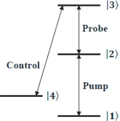
Angular quantum numberis defined as: = 0, so that the transitions are in S subshell. Since electric field stress and strain are high in Wurtzite structures in III-nitride compounds, the effects of piezoelectric and spontaneous polarization and also exchange potential due to exchange correlation are added to the total potential. In the modulator structure shown in Fig. 2, the wells are GaN, since the electron should be in ground state under equilibrium conditions, the barriers chosen from n-doped AlN. After creating the 4-level structure and inserting pump, probe and also control signal to apply electromagnetically induced transparency (EIT) to enhance the modulator speed (Fig. 3), the corresponding time evolution density matrix equations for four-level system is considered as [12]:
˙
ρ11=−i
Ω12
2
ρ12eiΔ12t−ρ21e−iΔ12t
+γ21ρ22+γ31ρ33+γ41ρ44.
˙
ρ22=−i
Ω23
2
ρ23eiΔ23t−ρ32e−iΔ23t
−iΩ12
2
ρ21e−iΔ12t−ρ12eiΔ12t
+γ32ρ33−γ21ρ22−γ24ρ22.
˙
ρ33=−i
Ω23
2
ρ32e−iΔ23t−ρ23eiΔ23t
−iΩ34
2
ρ34e−iΔ34t−ρ43eiΔ34t
−ρ33(γ32+γ31+γ34).
˙
ρ44=−i
Ω34
2
ρ43eiΔ34t−ρ34e−iΔ34t
+γ34ρ33−γ41ρ44+γ24ρ22.
˙
ρ12=−i
Ω12
2 (ρ11−ρ22)e
−iΔ12t−iΩ23
2 ρ13e
iΔ23t−ρ12
2 (γ21+γ24).
˙
ρ23=−i
Ω23
2 (ρ22−ρ33)e
−iΔ23t+iΩ12
2 ρ13e
iΔ12t−iΩ34
2 ρ24e
−iΔ34t−ρ23
2 (γ32+γ31+γ21+γ34+γ24)
˙
ρ24= i
Ω23
2 ρ34e
−iΔ23t+iΩ12
2 ρ14e
iΔ12t−iΩ34
2 ρ23e
iΔ34t−ρ24
2 (γ24+γ21+γ41)
˙
ρ34=−i
Ω34
2 (ρ33−ρ44)e
iΔ34t+iΩ23
2 ρ24e
iΔ23t−ρ34
2 (γ32+γ31+γ34+γ41)
˙
ρ31=−i
Ω12
2 ρ32e
iΔ12t+iΩ23
2 ρ21e
iΔ23t+iΩ34
2 ρ41e
iΔ34t−ρ31
2 (γ32+γ31+γ34)
˙
ρ41= i
Ω34
2 ρ31e
−iΔ34t−iΩ12
2 ρ42e
iΔ12t−ρ41
2 (γ41)
(2)
Here, Δ12 = ω12−ν12, Δ23 = ω23−ν23 and Δ34 = ω34−ν34 denote the detunings related to pump,
(a) (b)
Figure 1. (a) Two-dimentional profile for a multilayer spherical quantum dot and (b) related potential profile along the QD radius [12].
Figure 2. Energy diagram of spherical quantum dot structure in conduction band along the QD radius. (The barriers are from n-doped AlN and the wells are GaN) [12].
absorption, transmission and modulation depth, the linear susceptibility is calculated. The absorption is related to the imaginary section of linear susceptibility. All the equations, flowchart, tables and related items were presented in detail in our last work [12].
χ= P
ε0E
= 2Na℘
2ρ 23
ε0Ω23
(3)
In this modulator probe signal is modulated by the variation of carriers population in state |2. In other words, pump light changes the electrons population in this state and modulates the probe through absorption process. The important characteristic of this device in contrast to its rivals [7–10] is its ultrafast operation due to applying EIT method to conduct the carriers to state |4 and finally to ground state with fast decay. All three lights, i.e., pump, probe and control are applied to a four-level system as shown in Fig. 3 and tuned on 1480 nm, 1570 nm and 1324 nm, respectively. Regarding the high effect of confinement factor in modulator operation, the normal amount for every tenfold layer of quantum dots is Γ = 0.015 and the QD layers repetition number as: N = 95 [13]. Considering transmission matrix method (TMM), the extracted reflection for this structure isR= %10.
Figure 3. Proposed four-Level system equivalent to quantum dot modulator structure [12].
Figure 4. Schematic of optical fiber and modulator (waveguide) structure, (quantum dots are located in GaN core in the waveguide).
this purpose the distribution of the electric field in optical fiber and modulator must be obtained. The overall geometry of the structure is shown in Fig. 4. By calculating the amount of optical coupling (η) between the two elements, the insertion loss can be calculated. With extracting the fiber and waveguide fields and calculating their overlap integral, the optical coupling will be calculated [14, 15]. If ψ1 and
ψ2 are the field equations in fiber and modulator, the optical coupling is as follows, and consequently
insertion loss is: IL= 1−η
η=
ψ1ψ2∗dxdy
ψ21dxdy
1/2
ψ22dxdy
1/2 (4)
3. SIMULATIONS AND RESULTS
In order to evaluate the modulator performance and behavior, the values for variables are as follows: the probe beam intensity is equal to 1 mw, i.e.,Iprobe = 1.7×10³ (Wcm−2) and tuned on 1570 nm, the
pump intensity as: Ipump= 5×10⁸ (Wcm−2) and the intensity of the control signalIcontrol = 1.2×10²
(Wcm−2). The carrier density: N
a = 8×10¹⁸ (cm−3) and temperature is: T = 300 K. The number of repetitions of the layers of the quantum dots is assumed: I2 = 1.5×10⁸. The carrier relaxation
electric fields profile in the fiber and waveguide according to the corresponding equations are obtained based on the physical characteristics of the structure and boundary conditions. In this structure, the refractive indices of doped Sio2 as the core and cladding of the optical fiber are respectively equal to
n1 = 1.46 andn2 = 1.45, and the fiber core radius is equal toa= 5µm. Assuming optical fiber in the
form of a single-mode fiber with a step refractive index, the obtained light field in fiber is the first kind Bessel function [15]. The Marcatili’s method was also used to calculate optical profile in the waveguide with step refractive index [14, 15]. In this analysis, in accordance with the previous figure, the quantum dots are located in the GaN channel with refractive indexn1 = 2.3 and are enclosed by a layer of AlN
with n2 = 2.2. Also, the width (W) and height (T) of the waveguide are considered equal (W = T).
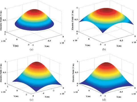
Taking into account Expq (TM-like mode in modulator, the electric field profile for fundamental mode in fiber in the first kind Bessel is shown in Fig. 5(a). Also the light profiles in modulator for different dimensions, i.e., x =y= 1, 5, 10µm, are shown in Figs. 5(b), (c), (d). In the modulator in Fig. 5(b) with dimension of x = y = 1µm, the light field is almost uniform, and by increasing the waveguide dimension to x =y= 5µm and x=y = 10µm, the field profile decreases and reaches to near zero at the corners of the waveguide (Figs. 5(c), (d)).
Computing the overlapping integrals associated with these two fields and assuming the displacement distance (D) as the displacement in one of the x or y directions between the fiber and modulator
(a) (b)
(c) (d)
Figure 5. Electric field profile for (a): optical fiber with radius a = 5µm and modulator with dimensions: (b) x = y = 1µm, (c) x = y = 5µm, (d) x = y = 10µm, refractive index of core and cladding for optical fiber aren1 = 1.46 andn2= 1.45 and for waveguide aren1 = 2.3 andn2= 2.2
(a) (b)
(c)
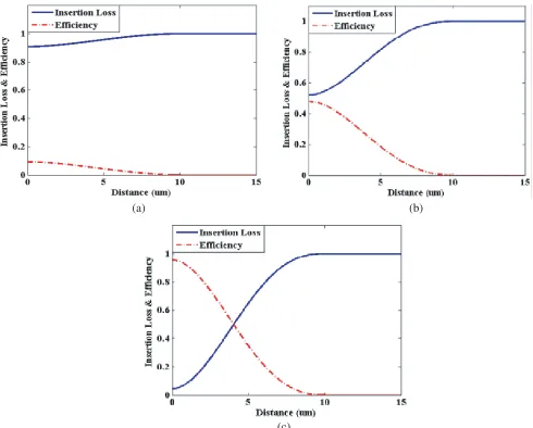
Figure 6. Input coupling efficiency and insertion loss vs. displacement distance between fiber with radius a= 5µm and modulator for different dimension: (a) x =y = 1µm, (b) x =y = 5µm and (c)
x=y= 10µm, refractive index of core and cladding for optical fiber aren1 = 1.46 andn2 = 1.45 and
for waveguide are n1 = 2.3 and n2 = 2.2 respectively.
(mismatching), the input coupling efficiency and the insertion loss in terms of the displacement distance for the different dimensions of the waveguide are displayed in Fig. 6.
It is seen that in the distance ofD= 0µm, there are the highest efficiency and lowest insertion loss, but with increasing displacement, the insertion loss is increased and atD= 10µm reaches its maximum. To compare different dimensions of the modulator, in Fig. 6(a) it seems that for the dimensions of
x = y = 1µm the insertion loss is very high, so even for the displacement of D = 0µm this value reaches 0.9, and forx=y= 5µm in Fig. 6(b) this value is about 0.5, while this amount is negligible for the dimension of x =y = 10µm (Fig. 6(c)). In other words, with respect to the fiber core radius, by decreasing the modulator dimensions, losses increase dramatically which makes it difficult for modulator function. Now consider that the displacement between the fiber and the modulator is constant, the coupling efficiency and insertion loss versus the waveguide dimensions are plotted in Fig. 7. It is seen that with increasing waveguide dimensions, the value of insertion loss is decreased, and for dimensions of 10µm it is less than 0.1.
Figure 7. Coupling efficiency and insertion loss vs. the modulator dimensions forD= 0.5µm refractive index of core and cladding for optical fiber aren1= 1.46 andn2 = 1.45 and for waveguide aren1= 2.3
and n2= 2.2 respectively.
(a) (b)
(c)
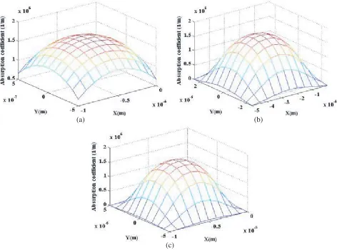
Figure 8. Absorption coefficient for waveguide dimensions: (a) x =y = 1µm, (b) x=y = 5µm, (c)
x=y= 10µm,Ipump= 5×10⁸(Wcm−2),Iprobe = 1.7×10³ (Wcm−2) andIcontrol= 1.2×10²(Wcm−2).
Periods of QD layers, density of carriers, Reflection, and temperature are,N = 95,Na= 8×10¹⁸(cm−3),
characteristics of the modulator is considerable. As the pump power has the main effect on modulator operation, by reducing the pump power toward the waveguide side walls, probe modulation will be disturbed. In Fig. 8 it is observed that the absorption becomes weak with decreasing the pump power along the waveguide side walls.
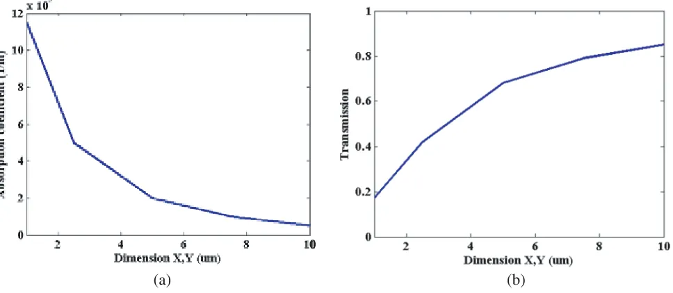
It is noticeable that in Fig. 8(a) the absorption coefficient is almost uniform in the channel waveguide withx=y= 1µm, but in Fig. 8(b) for dimension ofx=y= 5µm the absorption is near zero by the side walls, and in the modulator with the dimensions of 10µm, by approaching to the waveguide walls, the electric field becomes weak much more than other dimensions and reaches zero (Fig. 8(c)). Therefore, in a modulator with dimensions of 10µm the pump intensity, near the walls, is very close to zero, so the probe absorption will reach zero. However in modulator with x =y = 1µm, the field and absorption are almost uniform in the waveguide. The absorption and transmission coefficient near the walls are presented vs. the dimensions of the modulator for different amounts: x=y= 1, 2.5, 5, 7.5, 10µm in Fig. 9. It should be noted that with increasing dimensions of the modulator, the absorption near the walls has dropped dramatically (Fig. 9(a)), and transmission coefficient goes up noticeably (Fig. 9(b)). This
(a) (b)
0
Figure 9. (a) absorption and (b) transmission vs. the waveguide dimensions for different amounts:
x=y = 1, 2.5, 5, 7.5, 10µm refractive index of core and cladding for optical fiber aren1 = 1.46 and
n2= 1.45 and for waveguide are n1= 2.3 andn2 = 2.2 respectively.
(c)
Figure 10. Modulation depth for dimensions: (a)x=y= 1µm, (b)x=y= 5µm, (c)x=y= 10µm,
Ipump = 5×10⁸ (Wcm−2), Iprobe = 1.7×10³ (Wcm−2) and Icontrol = 1.2×10² (Wcm−2). Periods
of QD layers, density of carriers, Reflection, and temperature are, N = 95, Na = 8×10¹⁸ (cm−3),
R= %10T = 300 K.
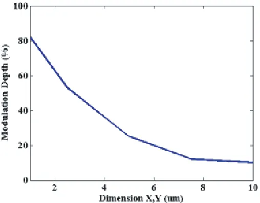
matter shows that modulator operation has high efficiency in the central region of the waveguide. The same situation is shown in Fig. 10 for depth of modulation. As we can see, with increasing dimensions of the modulator, the modulation depth decreases near the walls, and the modulation process uniformity becomes weak. One can see in Fig. 10(a) that the modulation depth is almost the same in the channel with x = y = 1µm, but in Fig. 10(b) for dimensions of x = y = 5µm, modulation depth becomes low near the side walls and for x =y = 10µm is very weak at the corners (Fig. 10(c)). The depth of modulation vs. the channel size is shown in Fig. 11. The modulation depth decreases along the sides of the channel walls, and it reaches 10% for the dimensions of 10µm, indicating modulator performance impairment in that area.
Figure 11. Modulation depth vs. the modulator dimension for different amounts: x = y = 1, 2.5, 5, 7.5, 10µm refractive index of core and cladding for optical fiber are n1= 1.46 and n2 = 1.45
4. CONCLUSION
In this paper, proper characteristics of a waveguide as an all optical modulator are presented, and the roles of insertion loss and light profiles in the waveguide on the operation of the modulator including absorption and depth of modulation are considered. The effects of modulator dimensions on the insertion loss and light profile are also investigated, and some discussions are conducted on the appropriate dimensions. The results show that in modulator with dimensions of 1µm, the light profile and consequently absorption and modulation process are uniform in the waveguide but give a significant increase in the insertion loss which disturbs the modulator performance. On the other hand, using a modulator with dimension of 10µm, the modulation is not uniform, but insertion loss is negligible. So a modulator with dimensions of 10µm will be a proper choice in contrast to other dimensions.
REFERENCES
1. Nevou, L., F. H. Julien, R. Colombelli, F. Guillot, and E. Monroy, “Room-temperature intersubband emission of GaN/AlN quantum wells atλ= 2.3µm,” Electron. Lett., Vol. 42, 1308– 1309, 2006.
2. Hamazaki, J., S. Matsui, H. Kunugita, K. Ema, H. Kanazawa, T. Tachibana, A. Kikuchi, and K. Kishino, “Ultrafast intersubband relaxation and nonlinear susceptibility at 1.55µm in GaN/AlN multiple-quantum wells,” Appl. Phys. Lett., Vol. 84, 1102–1104, 2004.
3. Friel, I., K. Driscoll, E. Kulenica, M. Dutta, R. Paiella, and T. D. Moustakas, “Investigation of the design parameters of AlN/GaN multiple quantum wells grown by molecular beam epitaxy for intersubband absorption,”J. Cryst. Growth, Vol. 278, 387–392, 2005.
4. Nevou, L., M. Tchernycheva, L. Doyennette, F. H. Julien, E. Warde, R. Colombelli, F. Guillot, S. Leconte, E. Monroy, T. Remmele, and M. Albrecht, “New developments for nitride unipolar devices at 1.3–1.5µm wavelengths,” Superlattices Microstruct., Vol. 40, 412–417, 2006.
5. Gopal, A. V., H. Yoshida, A. Neogi, N. Georgiev, T. Mozume, T. Simoyama, O. Wada, and H. Ishikawa, “Intersubband absorption saturation in InGaAs-AlAsSb quantum wells,” IEEE J. Quantum Electron., Vol. 38, 1515–1520, 2002.
6. Akimoto, R., B. S. Li, K. Akita, and T. Hasama, “Subpicosecond saturation of intersubband absorption in (CdS/ZnSe)/BeTe quantum well waveguides at telecommunication wavelength,” Appl. Phys. Lett., Vol. 87, 181104, 2005.
7. Sun, H. H., F. Y. Guo, D. Y. Li, L. Wang, D. B. Wang, and L. C. Shao, “Intersubband absorption properties of high Al content AlxGa1−xN/GaN multiple quantum wells grown with different
interlayers by metal organic chemical vapor deposition,” Nanoscale Research Letters, Vol. 7, 1– 6, 2012.
8. Neogi, A., H. Yoshida, T. Mozume, N. Georgiev, and O. Wada, “Intersubband transition and ultrafast all-optical modulation using multiple InGaAs-AlAsSb-InP coupled double-quantum-well structures,”IEEE J. Sel. Top. Quantum Electron., Vol. 7, 7, 2001.
9. Chen, G., X. Q. Wang, X. Rong, P. Wang, F. J. Xu, N. Tang, Z. X. Qin, Y. H. Chen, and B. Shen, “Intersubband transition in GaN/InGaN multiple quantum wells,” Sci. Rep., Vol. 5, 11485, 2015. 10. Fu, H., Z. Lu, X. Huang, H. Chen, and Y. Zhao, “Crystal orientation dependent intersubband
transition in semipolar AlGaN/GaN single,”App. Phys., Vol. 119, 174502, 2016.
11. Rostami, A., H. Baghban, and H. Rasooli Saghai, “An ultra-high level second-order nonlinear optical susceptibility in strained asymmetric GaN-AlGaN-AlN quantum wells: Towards all-optical devices and systems,”Microelectronics J., Vol. 38, 900, 2007.
12. Rahmani, A. and A. Rostami, “Ultrafast GaN/AlN modulator based on quantum dot for terabit all-optical communication,” Optik, Vol. 125, 3844, 2014.
14. Nishihara, H., M. Haruna, and T. Suhara,Optical Integrated Circuits, 29, 89, McGraw-Hill, USA, 1985.
![Figure 2. Energy diagram of spherical quantum dot structure in conduction band along the QD radius.(The barriers are from n-doped AlN and the wells are GaN) [12].](https://thumb-us.123doks.com/thumbv2/123dok_us/1974154.1260613/3.612.129.492.83.222/figure-energy-diagram-spherical-quantum-structure-conduction-barriers.webp)