Available online: https://edupediapublications.org/journals/index.php/IJR/ P a g e | 5 9 7 ABSTRACT: In this paper, a novel
architecture of A.E.S algorithm using high security technique for the VLSI implementation for AES algorithm. The pre-defined keys are required for each input for both encryption and decryption of the AES algorithm that are generated in real-time by the key-scheduler module by expanding the initial secret key and thus used for reducing the amount of storage for buffering. For high security we are proposing shift row mix column technique. The pipelining is used after each standard round makes fast of operation to enhance the throughput and shift row mix column.
INTRODUCTION
Several techniques such as cryptography, watermarking and scrambling have been developed to keep data secure, private, and copyright protected [1]. Cryptography is an essential tool underlying virtually all networking and computer protection traditionally used for military. However, the need for secure transactions in e-commerce, private networks, and secure message has moved encryption into the commercial way.
Communication / transfer of data in the present days invariably necessitate the use of encryption. It is also used in Military and Government’s communication, Encryption is also used for protecting many kinds of civilian services such as
Data encryption is achieved by a systematic algorithm called encryption. An encryption algorithm provides Confidentiality and Authentication. Confidentiality is the requirement that information is kept secret from people who are not permit to access it. Authentication is the process that the message indeed originates from the sender.
Integrity is also used to require that information is unaltered and that information “is modified only by those users who have the right to do so.” Nonrepudiation means that the sender or receiver of a message cannot permit to having sent or received the message.
Advanced encryption standard (AES) was issued at Federal Information Processing Standards (FIPS) by National Institute of Standards and Technology (NIST) as a successor to data encryption standard (DES) algorithms. In recent literature, a number of various architectures for the VLSI implementation of AES Rijndael algorithm are reported [6], [7], [8]. It can be observed that some of these architectures are low performance and some provide high area. Further, many of the architectures are not area efficient but it having higher cost when implemented in silicon.
An A.E.S M-Algorithm Using High Byte Sub Trans S.R Technique
G. SARANYA
[M.Tech – E.S & V.L.S.I]
CHEBROLU ENGINEERING COLLEGE
GUNTUR
A. RAGHAVA RAJU
ASSOCIATE PROFESSOR
CHEBROLU ENGINEERING COLLEGE
GUNTUR
Available online: https://edupediapublications.org/journals/index.php/IJR/ P a g e | 5 9 8
In this paper, a novel architecture of A.E.S algorithm using high security technique that is suitable for optimized for high throughput in terms of the encryption and decryption data rates using pipelining.
FIG. 1 Algorithm of Encryption and Decryption
We used the tower field approach for the S-box and we adapted the number of shares for each function in the S-box computation to minimize the overall gate count of the S-box. We used only two shares for most of the linear operations and hence had two sets of registers for state update and key schedule. All functions were uniformly shared and the number of shares went up to five in the S-box. We used remasking to satisfy the uniformity in the whole circuit when the uniformly shared functions are combined. Our practical security evaluation confirmed the expected first-order DPA resistance and identified the linear part in two shares as the most vulnerable part of the implementation.
In this extended version, we investigate the uniformity problem and the need for remasking in more detail. We prove that under certain circumstances, it is enough to remask only a fraction of the shares. Moreover, we argue that if there is enough remasking, we do not need to share
functions uniformly. This observation helps us to further reduce the area and randomness requirements. We provide two new implementations.
The first one is similar to the one in, but it uses at least three shares in all the operations, including the linear ones. We use it to investigate the increase in security when moving from at least two to at least three shares, and to quantify the associated cost. The second implementation is based on the one in but modified according to our findings regarding uniformity and remasking. It requires only about 8 BITS with the library that we use and 32 bits of additional randomness per S-box calculation. Our three implementations need the same number of clock cycles to complete the calculation, and allow us therefore to focus on some trade-offs between area and additional randomness.
Available online: https://edupediapublications.org/journals/index.php/IJR/ P a g e | 5 9 9
Fig.2 A.E.S Block Diagram
The data unit consists of: the initial round of key addition and a final round. The architecture of a standard round composed of both the transformation and the inverse transformation needed for encryption and decryption respectively are performed using the same hardware resources. This implementation generates one set of sub key and reuses for calculating all other subkeys in real-time.
1. Byte Sub: In this architecture each block is replaced by the substitution in S-Box table consisting of the byte of the block. 2. Shift Row: In this transformation the rows of the block state are shifted over different offsets. The amount of shifts is determined by the block length. The proposed architecture implements the shift row operation using combinational logic considering the offset by which a row should be shifted.
3. Mix Column: The mix column in encryption and decryption done the columns to be mix and inverse of column mixing respectively.
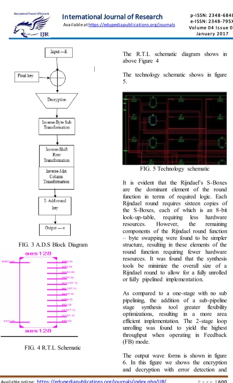
In the Advance decryption process is shown in figure 3 and the total operations in the A.E.S is inverse the operations like inverse byte sub transformation, inverse shift row , inverse mix column. The output of A.E.S is “E” it is given to input for A.D.S and the output of A.D.S is equal to the input of A.E.S.
Available online: https://edupediapublications.org/journals/index.php/IJR/ P a g e | 6 0 0
FIG. 3 A.D.S Block Diagram
FIG. 4 R.T.L Schematic
The R.T.L schematic diagram shows in above Figure 4
The technology schematic shows in figure 5.
FIG. 5 Technology schematic
It is evident that the Rijndael’s S-Boxes are the dominant element of the round function in terms of required logic. Each Rijndael round requires sixteen copies of the S-Boxes, each of which is an 8-bit look-up-table, requiring less hardware resources. However, the remaining components of the Rijndael round function – byte swapping were found to be simpler structure, resulting in these elements of the round function requiring fewer hardware resources. It was found that the synthesis tools be minimize the overall size of a Rijndael round to allow for a fully unrolled or fully pipelined implementation.
As compared to a one-stage with no sub pipelining, the addition of a sub-pipeline stage synthesis tool greater flexibility optimizations, resulting in a more area efficient implementation. The 2-stage loop unrolling was found to yield the highest throughput when operating in Feedback (FB) mode.
Available online: https://edupediapublications.org/journals/index.php/IJR/ P a g e | 6 0 1
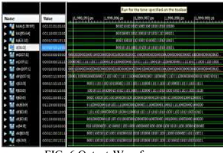
correction. The errors in the decryption is overcome by using this architecture.
FIG. 6 Output Waveform
The no. of slices , L.U.T’s and IOB’S shows in below tabular form 1
Table 1 Summary report
CONCLUSION
We have presented a VLSI architecture for the Rijndael AES algorithm that performs both the encryption and decryption. The S-boxes are used for the implementation of the S.R, M.C and inverses S.R & M.C shared between encryption and decryption. The round keys needed for each round of the implementation are generated in real-time. The initial and final key scheduling is implemented on the same device, thus allowing efficient area minimization. The implementation of the key unit in the proposed architecture, can be scaled for the keys of length 256 bits. The total delay to implement this architecture is 20.742 ns and memory used is 210912kb.
REFERENCES
[1] K. Fu and J. Blum, “Controlling for cybersecurity risks of medical device software,” Commun. ACM, vol. 56, no. 10, pp. 35–37, Oct. 2013.
[2] D. Halperin, T. Kohno, T. S. Heydt-Benjamin, K. Fu, and W. H. Maisel, “Security and privacy for implantable medical devices,” IEEE Pervasive Comput., vol. 7, no. 1, pp. 30–39, Jan./Mar. 2008.
[3] M. Rostami, W. Burleson, A. Jules, and F. Koushanfar, “Balancing security and utility in medical devices?” in Proc. 50th ACM/EDAC/IEEE Int. Conf. Design Autom., May/Jun. 2013, pp. 1–6.
[4] M. Zhang, A. Raghunathan, and N. K. Jha, “Trustworthiness of medical devices and body area networks,” Proc. IEEE, vol. 102, no. 8, pp. 1174–1188, Aug. 2014. [5] H. Khurana, M. Hadley, N. Lu, and D. A. Frincke, “Smart-grid security issues,” IEEE Security Privacy, vol. 8, no. 1, pp. 81–85, Jan./Feb. 2010.
[6] M. Mozaffari-Kermani, M. Zhang, A. Raghunathan, and N. K. Jha, “Emerging frontiers in embedded security,” in Proc. 26th Int. Conf. VLSI Design, Jan. 2013, pp. 203–208.
[7] R. Roman, P. Najera, and J. Lopez, “Securing the Internet of things,” Computer, vol. 44, no. 9, pp. 51–58, Sep. 2011.
[8] T. H.-J. Kim, L. Bauer, J. Newsome, A. Perrig, and J. Walker, “Challenges in access right assignment for secure home networks,” in Proc. USENIX Conf. Hot Topics Secur., 2010, pp. 1–6.
Available online: https://edupediapublications.org/journals/index.php/IJR/ P a g e | 6 0 2