PERFORMANCE EVALUATION OF 1.25×16 GB/S
BIDIRECTIONAL DWDM PASSIVE OPTICAL
NETWORK BASED ON CYCLIC AWG
Arashdeep Kaur
1, Ramandeep Kaur
2 1Student, M.Tech, Department of Electronics and Communication Engineering,
Punjabi University Patiala, (India)
2
Assistant Professor, Department of Electronics and Communication Engineering,
Punjabi University Patiala, (India)
ABSTRACT
We proposed and experimentally demonstrated the cyclic array waveguide grating based bidirectional dense
wavelength division multiplexing passive optical network. In the proposed scheme the downstream signal were
produced by a wavelength division multiplexing transmitter. The 16 channel proposed network works with 1.25
Gbps downstream signal bit rate and 655 Mbps upstream signal bit rate. The system was proposed over 30 km
distance between OLT and ONT using 100 GHz channel spacing in a bidirectional single mode fiber and cyclic
array waveguide gratings.
Keywords: Array waveguide grating (AWG), Bit error rate (BER), Dense wavelength division
multiplexing Passive Optical Network (DWDM PON), Optical line terminal (OLT), Optical network
terminal (ONT).
I. INTRODUCTION
To support the explosive growth of data traffic, various types of wavelength-division-multiplexed passive optical networks (WDM PONs) have been proposed and demonstrated [1]–[5]. This is because WDM PON is attractive due
to its large capacity, easy management, network security, and upgradability. However, the network complexity and
its subsequent cost have been the most critical issues for the practical deployment. To overcome this problem, it has
been proposed to implement WDM PON by using spectrum-sliced incoherent light sources such as light-emitting
diodes (LEDs) and amplified spontaneous emission sources [1], [2]. The advantage of such a network would be the
use of identical light source at every subscriber site. In addition, these networks could be robust to the optical
crosstalk and the temperature-induced drift of the arrayed-waveguide grating (AWG) placed at the remote node
(RN) [3], [4]. However, when the spectrum-slicing technique is used, it is often difficult to secure an adequate
amount of system margin due to the large slicing loss and low output power of LED. This problem could be relaxed
to some extent by using high-power LEDs and sensitive receivers such as avalanche photodiodes (APDs). To solve
demonstrate a bidirectional WDM PON using a WDM transmitter. The spectrum-slicing has been achieved
automatically at the AWG used for multiplexing and demultiplexing WDM channels. However, when we use cyclic
AWG, the spectrum-sliced light would have multiple peaks separated by the free-spectral-range (FSR) of the AWG.
Previously, only one of these peaks was selected and used for the transmission to avoid excessive dispersion penalty
[1], [2]. However in the proposed BPON network, we have used a 16 channel WDM transmitter with NRZ (non
return to zero) modulation format. In the proposed system extinction ratio (ER) of 4 dB has been used with bit rate
of 1.25 Gb/s for the downstream signal. In the proposed structure the WDM transmitter has been operated on 1550
nm frequency range with channel spacing of 0.8 nm. For the proposed BPON the upstream signal frequency range
of 1360 nm was used with ER 4 dB and channel spacing 0.8 nm. For the upstream signal the system operated with
655 Mbps bit rate. We believe that proposed network could be cost effective due to the use of multiple peaks of
spectrum sliced light and bidirectional transmission.
II.DWDM-PON
STRUCTURE
AND
RESULTS
2.1
Proposed Structure
Figure 1 shows the proposed DWDM PON structure. The downstream signals generated by the WDM transmitter in
the central office (CO) were multiplexed by the bidirectional Array waveguide grating (AWG) and were fed to a
bidirectional SMF (single mode fiber) of 30 KM. After passing through the bidirectional SMF, the signal passes
through another cyclic AWG that acts as demultiplexer for downstream signal. The output signals of cyclic AWG
were fed at the input of PIN photodiodes. In the receiver section PIN photodiodes has been followed by buffer
selectors and BER (bit error rate) analyzers to observe the output. We have used 16 optical transmitters to produce
the upstream signals in the ONT section, having 1360 nm to 1348 nm wavelength with 0.8 nm channel spacing. The
upstream signals multiplexed by the cyclic AWG have been passed through bidirectional SMF. The cyclic AWG
that multiplexes the downstream channels also demultiplexes the upstream channels. By using BER analyzers we
observed outputs of demultiplexed upstream signals by using the same PIN photodiodes as used in the OLT section.
2.2 Characteristics of Cyclic Array Waveguide Grating
Arrayed Waveguide Grating (AWG) multiplexers/demultiplexers are planar devices which are based on an array of
waveguides with both imaging and dispersive properties. The operation can be understood as follows [6]. When a
beam propagating through the transmitter waveguide enters the first Free Propagation Region (FPR) it is no longer
laterally confined and becomes divergent. On arriving at the input aperture the beam is coupled into the waveguide
array and propagates through the individual waveguides towards the output aperture. The divergent beam at the
input aperture is thus transformed into a convergent one with equal amplitude and phase distribution, and the input
field at the object plane gives rise to a corresponding image at the centre of the image plane. The spatial separation
of different wavelengths is obtained by linearly increasing the lengths of the array waveguides, which introduces a
wavelength dependent tilt of the outgoing beam associated with a shift of the focal point along the image plane. If
receiver waveguides are placed at proper positions along the image plane, different wavelengths are led to different
output ports. Focusing of the fields propagating in an AWG is obtained if the length difference ∆L between adjacent
waveguides is equal to an integer number m of wavelengths inside the AWG:
(1)
The integer m is called the order of the array, λc is the central wavelength (in vacuum) of the AWG, neff is the
effective refractive (phase) index of the guided mode, and λc/neffcorresponds to the wavelength inside the array
waveguides.
The length increment ∆L of the array gives rise to a phase difference according to
(2)
Where
(3)
is the propagation constant in the waveguides, v = c/λ is the frequency of the propagating wave, and c is the speed of
light in vacuum. The lateral displacement ds of the focal spot along the image plane per unit frequency change dv is
called the spatial dispersion Dsp of the AWG, which is given by [7]:
(4)
Where nFPR is the (slab) mode index in the Free Propagation Region, ∆ is the divergence angle between the array
waveguides in the fan-in and the fan-out sections, and ng is the group index of the waveguide mode:
(5)
The period in the frequency domain is called the Free Spectral Range (FSR), and
∆
in combination with (1) leads to:
FSR
(
)
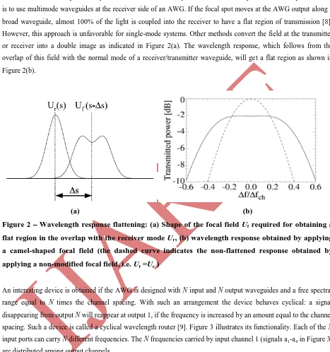
(6)An important feature of the AWG-filter characteristics is the passband shape. Flattened and broadened channel
transmissions are an important requirement for AWG de/multiplexers. To flatten the passband the simplest method
is to use multimode waveguides at the receiver side of an AWG. If the focal spot moves at the AWG output along a
broad waveguide, almost 100% of the light is coupled into the receiver to have a flat region of transmission [8].
However, this approach is unfavorable for single-mode systems. Other methods convert the field at the transmitter
or receiver into a double image as indicated in Figure 2(a). The wavelength response, which follows from the
overlap of this field with the normal mode of a receiver/transmitter waveguide, will get a flat region as shown in
Figure 2(b).
(a)
(b)
Figure 2 – Wavelength response flattening: (a) Shape of the focal field
U
f required for obtaining aflat region in the overlap with the receiver mode
U
r, (b) wavelength response obtained by applyinga camel-shaped focal field (the dashed curve indicates the non-flattened response obtained by
applying a non-modified focal field, i.e.
U
f =U
r )An interesting device is obtained if the AWG is designed with N input and N output waveguides and a free spectral
range equal to N times the channel spacing. With such an arrangement the device behaves cyclical: a signal
disappearing from output N will reappear at output 1, if the frequency is increased by an amount equal to the channel
spacing. Such a device is called a cyclical wavelength router [9]. Figure 3 illustrates its functionality. Each of the N
input ports can carry N different frequencies. The N frequencies carried by input channel 1 (signals a1-a4 in Figure 3)
are distributed among output channels.
The general AWG behavior is described by (7), where and represents the angles between the respective
slab centre axis and the attached input/output waveguides.
{
[
In this equation, λi is the signal wavelength and m is the grating order at λi, λc is the design centre wavelength at
order m, d is the grating pitch, and ns and nwg are the effective refractive indices at λc of the slab and the grating
waveguides, respectively. This equation takes into account also the chromatic material dispersion by a linear fit of
nwg around λc (given in square brackets). The input/output waveguide positions at both slabs are x= f, where f is the
slab focal length.
Fig. 3 Schematic diagram illustrating the operation of a wavelength router
2.3
Transmission performance
In the proposed system a 16 channel WDM transmitter produces the downstream signals in the 1500 nm range with
100 GHz channel spacing. An extinction ratio of 4 dB has been used for the downstream signal. WDM transmitter
produces the 16 downstream channels at input power of -3dBm. The driving amplitude was modulated by a
1.25Gbps non return to zero (NRZ) format. As the bit rate is enhanced from 1Gbps to 1.25Gbps and transmission
length is also increased from 10 km to 30 km [10].
Figure 6 – Eye diagram of downlink at 8dB
The signal power after the losses of two AWGs and bidirectional SMF was reduced to -13dBm before launching
into each ONU. The bidirectional single mode fiber has been operated with 16.75ps/nm/km dispersion and an
attenuation of 0.2dB/km. For producing the upstream signal the ONU has been composed of receiving module and
an optical transmitter that also operates with -3dBm input. Optical transmitter produces the same power signal as
produced by WDM transmitter at the OLT with extinction ratio of 4dB.
The receiving module for each channel at both OLT and ONT consists of a PIN photodiode, a Bessel filter, a 3R
generator and a BER analyzer. At 4dB extinction ratio Q-factor of 5.483 and bit error rate of 10-8 has been obtained
for downstream signal and for the upstream signal the Q-factor of 8.544 and bit error rate of 10-18 hase been
obtained. Figure 4, 5 and 6 show the eye diagrams for downstream signal at extinction ratio of 4dB, 6dB and 8dB
respectively. In eye diagram of figure 5 bit error rate of 10-9 and Q-factor of 5.849 has been obtained at 6dB ER.
And in eye diagram of figure 6 bit Error Rate of 10-10 and Q-factor of 6.03 has been obtained at 8dB ER. Figure 7
shows the relation between input power and BER at extinction ratio 4dB and 6dB and Figure 8 shows the relation
between input power and Q-factor.
Figure 7 – Relation between input power and Figure 8 – Relation between input power and
III.
C
ONCLUSIONThe bidirectional DWDM PON link using WDM transmitter and cyclic AWG was demonstrated and investigated.
The 16 channel bidirectional passive optical network has been operated on downstream bit rate of 1.25Gbps and the
upstream bit rate of 622Mbps. It is observed from the eye diagrams of figures 4, 5, and 6 that as the extinction ratio
was increased from 4 dB to 6 dB and 8 dB respectively the bit error rate and quality factor were improved.
Graphical representation in figures 7 and 8 shows the variation of downstream Bit error rate and Q-factor with
respect to the input power.
REFERENCES
[1] M. H. Reeve, A. R. Hunwicks, S. G. Methley, L. Bickers, and S. Hornung, “LED spectral slicing for single-mode local loop application,” Electron. Lett., vol. 24, pp. 389–390, Mar. 1988.
[2] D. K. Jung, S. K. Shin, C.-H. Lee, and Y. C. Chung, “Wavelength-division- multiplexed passive optical network
based on spectrum slicing techniques,” IEEE Photon. Technol. Lett., vol. 10, pp. 1334–1336, June 1998.
[3] Y. S. Jang, C.-H. Lee, and Y. C. Chung, “Effects of crosstalk in WDM systems using spectrum-sliced light
source,” IEEE Photon. Technol. Lett., vol. 11, pp. 715–717, June 1999.
[4] D. K. Jung, S. K. Shin, H. G. Woo, and Y. C. Chung, “Wavelength tracking technique for spectrum-sliced WDM
passive optical network,” IEEE Photon. Technol. Lett., vol. 12, pp. 338–340, Mar. 2000.
[5] K. H. Han, E. S. Son, K.W. Lim, H. Y. Choi, S. P. Jung, and Y. C. Chung, “Bi-directional WDM passive optical network using spectrum-sliced light-emitting diodes,” in Proc. Optical Fiber Communication (OFC 2004), Paper
MF98.
[6] C. van Dam: “InP-based polarization independent wavelength demultiplexers,” PhD thesis, Delft University of
Technology, Delft, The Netherlands (1997) ISBN90-9010798-3
[7] M.K. Smit and C. van Dam: “PHASAR-based WDM-devices: principles, design and applications,” J. Select.
Topics Quantum Electron. 2, 236–250 (1996)
[8] M. R.Amersfoort, C. R. de Boer, F. P. G. M. van Ham, M. K. Smit, P. Demeester, J. J. G. M. van der Tol, and A.
Kuntze: “Phased-array wavelength demultiplexer with flattened wavelength response,” Electron. Lett. 30, 300–
302 (1994)
[9] C. Dragone: “An N×N optical multiplexer using a planar arrangement of two star couplers,” IEEE Photon.
Technol. Lett. 3, 812–815 (1991)
[10] Fady I. El-Nahal, “Bidirectional WDM–PON architecture using a reflective filter and cyclic AWG”,