IJEDR1404054
International Journal of Engineering Development and Research (www.ijedr.org)3713
Low Transistor Count Scalable Digital Comparator
1
CH.Madhav,
2Shafee Unnisa Syed
1
M.Tech, 2Associate Professor,
1Electronics and Communication Engineering,
1Sreenidhi Institute of Science and Technology, Hyderabad, India
________________________________________________________________________________________________________
Abstract—Comparator is the most frequent operation in many digital and scientific applications. Here in this paper we are
simulating a low transistor count scalable digital comparator based on parallel prefix tree. Fastest comparators are designed by using the combinatorial logic gates, which results huge number of transistor count, and hence the area is also increased. So here we implemented the comparator using Gate Diffusion Input Cells to reduce the transistor count and hence the area of the circuit.
Index Terms - Comparator, Digital, Combinatorial logic, Gate Diffusion Input Cells, area
________________________________________________________________________________________________________ I.INTRODUCTION
Comparison is very frequent operation in many digital, Scientific Computations, and Data processing applications. A comparator compares two operands of length N, (An-1,An-2,…..A0 & Bn-1,Bn-2,…..B0 ) and produces the output as A>B, A<B and
A=B. The comparators are classified as Analog and Digital comparators. Here we are concentrating on digital comparators. Based on the outputs comparators are again classified as the equality only comparators which generates only equality condition and the other is full comparator which generates all three conditions. Others are mutual comparators which check for the equality of all the input bits. These mutual comparators are most widely used in memory bit comparisons.
Fastest comparators are designed by using the combinatorial logic gates. The drawback with this approach is it results in huge transistor count and hence the area of the circuit becomes large. However the transistor count is reduced by implementing the logic gates using Gate Diffusion Input (GDI) Cells. The use of parallel prefix tree ensures that reduced internal switching activities and parallelism so that the performance and energy efficiency is improved. The rest of the paper is organized as follows. Section II describes the existing comparator works. Sections III describes the architecture of parallel prefix tree structure based comparator architecture. Section IV describes the Gate Diffusion Input cell based Parallel Prefix Tree Comparator.
II.EXISTING COMPARATOR DESIGNS
Some of the comparator designs make use of dynamic logic gates to achieve high performance. Some of the designs as in [1] uses Prefix Tree Structures with MUX‟s, by taking the advantage of 1‟s complement addition, the draw back with this approach [1] is it produces either greater than (>) or less than (<), but not both, and also it consumes more power as most of the transistors are in ON state irrespective of the input. Some of the designs as in [2] make use of ANT (All-N-Transistor) logic to achieve high through put with multiple pipeline stages. The drawback of [2] this design is not suitable for single cycle processors. Some designs as in [3] make use of parallel prefix tree structure to reduce switching activity of internal signals, and to achieve parallelism so that the energy efficiency as well as performance is increased. In [3] the logic gates are implemented using the static CMOS cells, so the number of transistor count is increased drastically with the bit width and hence the area of the design also. Some designs [4] make use of priority encoding algorithms using multiple output domino logic to shorten logic path. This [4] design results in large conductive resistance [5].
III.PARALLEL PREFIX TREE COMPARATOR
The Parallel prefix tree structure improves the performance by achieving parallelism and reduces the energy consumption by reducing the switching activity of internal signals. The high level architecture of parallel prefix tree comparator [3] is shown in the Fig1. It comprises two modules at high end named as comparison module and decision module. The comparison module takes the two input operands A, B of length N and performs comparison asynchronously from MSB to LSB; because of this comparison logic is triggered only if all the bits of greater significance are equal. The intermediate outputs of the comparison module are stored in two buses left bus and right bus and are evaluated as follows:
If Ak>Bk then left-busk=1 and right-busk=0
If Ak<Bk then left-busk=0 and right-busk=1
If Ak=Bk then left-busk=0 and right-busk=0
IJEDR1404054
International Journal of Engineering Development and Research (www.ijedr.org)3714
Fig. 1. Block Diagram of Comparator ArchitectureIV.IMPLEMENTATION USING GATE DIFFUSION INPUT (GDI)CELLS
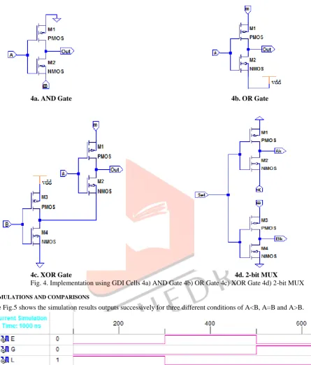
Gate Diffusion Input technique is a new low power design style. This allows implementing complex logic functions using only two transistors. As in [4] this technique results in reducing area, power consumption, propagation delay and number of devices. A basic Gate Diffusion Input cell [4] is shown in the fig 2. Table I shows various logic functions implemented using the GDI cell. All the functions of Table 1 can be implemented using Silicon-on-Insulator (SOI) or twin-well CMOS process [4]. This GDI technique is best suitable for fast implementation and low power applications of combinatorial circuits. Even though GDI cell looks like CMOS inverter it differs from the inverter in the following way.
1. The GDI Cell contains three inputs: The Common Gate Input of nMOS and pMOS (G), input to source/drain of nMOS (N) and input to source/drain of pMOS (P).
2. To arbitrarily bias the Bulks of both nMOS and pMOS are connected to N and P respectively.
Table I: Various Logic Functions implemented using GDI Cell
Fig. 2. A Basic GDI Cell
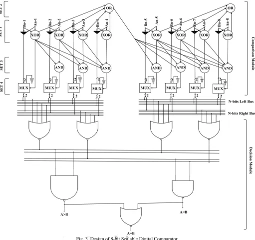
The Fig. 3 shows the design of 8-bit Scalable Digital Comparator based on parallel prefix tree structure. Each gate has a maximum fan-in and fan-out of five and 4 respectively independent of comparator bandwidth. The comparison module comprises of 4-sets of logic gates. Set-1 holds XOR gates with a maximum fan-in and fan-out of two and five respectively. These cells compute whether the computation has to terminate or not. The output of Set 1 is given as input to the Set 2 and Set 4 respectively. For any given k where the output of set is given as
(1)
Set 2 consists of OR gates with max fan-in and fan-out of 4. The out of Set 2 is given as input to Set3. These OR cells either continue the comparison of lesser significance bits if all four inputs are 0‟s otherwise terminate the comparison. For any given m where there is a total of OR cells functioning in parallel. The output of Set 2 is given as
∑ (2)
N P G Out Function
„0‟ B A ̅ B F1
B „1‟ A ̅ B F2
„1‟ B A A + B OR
B „0‟ A AB AND
C B A ̅ A C MUX
IJEDR1404054
International Journal of Engineering Development and Research (www.ijedr.org)3715
Fig. 3. Design of 8-bit Scalable Digital ComparatorSet 3 consists of AND gates with max fan-in and fan-out of 5 and 1 respectively. These AND cells receive inputs from Set 1 as well as Set2. The outputs of Set 3 control the MUX‟s which drives input to the left and right buses. The number of inputs to AND cells increases from left to right in for each bit and end up with maximum fan-in of five. The output of Set 3 for any given k where is given as
∏ (3)
Set 4 consists of two input 2-bit multiplexers who drive the input to the left-bus and right-bus. The select line of multiplexer is derived from the output of set3. Out of two inputs for multiplexer one is derived from input operands and the other is hardcoded as „00‟. If the select line is „0‟ then it will drive „00‟ to the buses otherwise „AkBk‟.
̅k× (00) (4)
Finally the input to left and right buses is given as input to the Decision Module which consists of two OR-networks (NOR followed by NAND). These OR networks compute the final result of A>B,A<B and from these two conditions A=B is derived.
IJEDR1404054
International Journal of Engineering Development and Research (www.ijedr.org)3716
4a. AND Gate 4b. OR Gate
4c. XOR Gate 4d. 2-bit MUX
Fig. 4. Implementation using GDI Cells 4a) AND Gate 4b) OR Gate 4c) XOR Gate 4d) 2-bit MUX
V.SIMULATIONS AND COMPARISONS
The Fig.5 shows the simulation results outputs successively for three different conditions of A<B, A=B and A>B.
Fig. 5. Simulation outputs for three different conditions A<B, A=B and A>B
Table II shows comparison number of transistor counts from implementing using static CMOS cells to Gate Diffusion Input (GDI) cells for comparison module. From this table it is noticed that the transistor count is reduced.
Table II: comparison of transistor count at various bit lengths of comparison module using Standard CMOS and GDI
Total Transistor Count 8-bit 16-bit 32-bit 64-bit
Using Standard CMOS Cells [3] 384 768 1424 2976
IJEDR1404054
International Journal of Engineering Development and Research (www.ijedr.org)3717
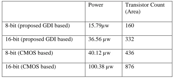
Table III shows comparison of power and number of transistor counts of the comparator using static CMOS cells to Gate Diffusion Input (GDI) cells at different bit-widths at 0.18 µm using spice simulation. From this table it is noticed that the power and transistor count is reduced.Table III: comparison of power and transistor count (area) for various bit widths
Power Transistor Count (Area)
8-bit (proposed GDI based) 15.79µw 160 16-bit (proposed GDI based) 36.56 µw 332
8-bit (CMOS based) 40.12 µw 436
16-bit (CMOS based) 100.38 µw 876
VI.CONCLUSION
From the above discussion it is concluded that the fastest comparators are made up of full combinatorial circuits. To reduce the switching activity of internal signals and to provide the parallelization parallel prefix tree structure is used. By implanting the design using static CMOS cells it results in large transistor count so that the area of the design in increased, by implementing using Gate Diffusion Input Cells power and transistor count, is reduced which result less area.
REFERENCES
[1] S.-W. Cheng, “A high-speed magnitude comparator with small transistor count,” in Proc. IEEE Int. Conf. Electron., Circuits, Syst., vol. 3, pp. 1168–1171, . Dec.2003.
[2] C.C. wang, C.F. Wu and K.C. Tsai, ”1 GHz 64-bit high-speed comparator using ANT dynamic logic with two-phase clocking” IEEE Proc. Comput. Digit. Tech., vol.145, no.6, pp.433-436, Nov 1998.
[3] Saleh Abdel-Hafeez, Ann Gordon-Ross, and Behrooz Parhami, “Scalable Digital CMOS Comparator Using a Parallel Prefix Tree,” Transactions on Very Large Scale Integration (VLSI) Systems, VOL. 21, NO. 11, pp. 1989-1998, Nov 2013.
[4] Arkadiy Morgenshtein, Alexander Fish, and Israel A. Wagner, “Gate Diffusion Input (GDI): A Power-Efficient Method for Digital Combinatorial Circuits,” IEEE Transactions on Very Large Scale Integration (VLSI) Systems, vol.10, No.5 pp. 566– 581, Oct 2002.