University of South Carolina
Scholar Commons
Theses and Dissertations
2017
Improved N-Type 4h-Sic Epitaxial Layer Radiation
Detectors and Noise Analysis of Front-End
Readout Electronics
Khai V. Nguyen University of South Carolina
Follow this and additional works at:https://scholarcommons.sc.edu/etd Part of theElectrical and Electronics Commons
This Open Access Dissertation is brought to you by Scholar Commons. It has been accepted for inclusion in Theses and Dissertations by an authorized administrator of Scholar Commons. For more information, please [email protected].
Recommended Citation
V. Nguyen, K.(2017).Improved N-Type 4h-Sic Epitaxial Layer Radiation Detectors and Noise Analysis of Front-End Readout Electronics.
I
MPROVEDN-T
YPE4H-S
IC
E
PITAXIALL
AYERR
ADIATIOND
ETECTORS ANDN
OISEA
NALYSIS OFF
RONT-
ENDR
EADOUTE
LECTRONICSby
Khai V. Nguyen
Bachelor of Science
University of South Carolina, 2013
Master of Engineering University of South Carolina, 2015
Submitted in Partial Fulfillment of the Requirements
For the Degree of Doctor of Philosophy in
Electrical Engineering
College of Engineering and Computing
University of South Carolina
2017
Accepted by:
Krishna C. Mandal, Major Professor
Enrico Santi, Committee Member
Guoan Wang, Committee Member
Yuriy V. Pershin, Committee Member
DEDICATION
I would like to dedicate this work to my dear wife, Lam, who has been a constant
source of support and encouragement in this endeavor. I am very thankful to have you by
ACKNOWLEDGEMENTS
First and foremost, I am sincerely grateful to my graduate advisor, Dr. Krishna C.
Mandal for welcoming me into his research group. His tremendous enthusiasm, guidance,
and support have enabled me to make great strides forward in my career and in my
understanding of semiconductors. He has continued to inspire my passion for science
from my first day in his class as an undergraduate electrical engineering student through
to this day. I would also like to thank my committee members, Dr. Enrico Santi, Dr.
Guoan Wang, and Dr. Yuriy V. Pershin for sacrificing a portion of their time to provide
guidance and support of my work.
I would like to thank the Chairman of the Department of Electrical Engineering,
Professor Roger Dougal, for his guidance and words of wisdom that set me on the path to
success in both life and as an engineer.
For their contributions in the research performed in this work, I would like to
thank the following people:
Dr. Sandeep K. Chaudhuri, for his extraordinary effort and tireless
patience invested in setting up the DLTS and passing on his knowledge of
radiation measurements and instrument calibration to me.
Dr. Shuguo Ma (College of Engineering and Computing, University of
The staff of the Institute for Electronics and Nanotechnology (IEN) at
Georgia Tech for organizing the equipment training schedule such that
two visits were enough to be qualified and added as a user for all of the
tools necessary for fabricating the edge-terminated detectors.
Nat Patterson, David London, Ashley Burt, Alicia Williams, David Metts,
Jenny Balestrero, Lauren Ridings and all those I have forgotten who have
provided both their expertise and kind words throughout my time here at
USC.
Finally, I would like to thank my fellow lab members, Dr. Sandeep K. Chaudhuri,
Dr. Sandip Das, Dr. Mohammad A. Mannan, Kelvin Zavalla, Cihan Oner, and Towhid A.
ABSTRACT
Schottky barrier radiation detectors were fabricated on n-type 4H-SiC
epitaxial layers (12 – 50 µm) grown by hot wall CVD process on highly nitrogen doped
4H-SiC (0001) substrates with 4-8º off-cut towards the ̅ direction. Ni/4H-SiC
Schottky barrier radiation detectors, a very low leakage current of 0.18 nA at 250 V bias,
revealing low thermal noise, was observed in current-voltage (I-V) measurements. Using
a thermionic emission model, junction properties such as barrier height of ≥1.10 eV and
an ideality factor of ≤1.29 were determined. An effective carrier concentration of
1.03×1015 cm-3 was calculated by capacitance-voltage (C-V) measurement. Deep level
transient spectroscopy (DLTS) was used to investigate electrically active defects in
epilayer. Defect parameters such as activation energy, capture cross-section, and density
of defects were calculated from Arrhenius plots. DLTS revealed the presence of shallow
level defects related to titanium impurities, electrically active lifetime killer Z1/2 defect,
and deep level defects assigned as EH6/7 which are related to carbon and carbon-silicon
vacancies. The density of Z1/2 defect, the most detrimental to detector performance, was
1.6×1012 cm-3, orders of magnitude lower compared to other 4H-SiC detectors.
Detector performances were evaluated in terms of the energy resolution at
full-width at half-maximum (FWHM) using pulse height spectroscopy (PHS) measurements
with 0.1 µCi 241Am source. Charge collection efficiency was investigated using a
was 166 keV with charge collection efficiency of 22.6%. Electronic noise analysis of
front-end readout system was carried out in terms of equivalent noise charge (ENC) in
order to study the contribution of white series noise, pink noise ( parallel and ⁄
series) and white parallel noise to the total electronic noise in the detection system.
New edge termination was developed using surface passivating layers of silicon
dioxide (SiO2) and silicon nitride (Si3N4) in order to improve detector performance. With
edge termination, reverse leakage current of Ni/4H-SiC epilayer detector was improved
significantly (nA to pA) leading to an increased signal-to-noise ratio. Improved Schottky
properties such as barrier height of ~1.7 eV and diode ideality factor of ~1.07 were
observed indicating a better surface uniformity that enhanced charge collection
efficiency. C-V measurement confirmed a doping concentration of 2.4 x 1014 cm-3
ensuring a fully depleted (~20 µm) detector at bias voltages as low as ~70 V. DLTS
analysis showed a decreased concentration of performance limiting Z1/2 defect level and
absence of EH6/7 deep-levels with edge termination, ensuing a more complete charge
collection. Alpha spectroscopy measurements revealed an improved detector energy
resolution from ~0.7% to ~0.4% for 5.48 MeV alpha particles with edge termination.
4H-SiC epitaxial detector with ruthenium (Ru) Schottky barrier contact (in
addition to Ni being used in above studies) was investigated for operation in harsh
environments with high temperature and high radiation. Ru/4H-SiC Schottky detectors
exhibited excellent rectification and improved junction properties, even without edge
termination. However, inhomogeneity of the Schottky barrier heights was observed due
to interfacial defects resulting from a solid-state reaction involving Ru, Si, and C. As a
alpha peaks were not resolved. The energy resolution was calculated to be ~ 0.75% at
TABLE OF CONTENTS
Dedication ... iii
Acknowledgements ... iv
Abstract ... vi
Table of Contents ... ix
List of Tables ... xii
List of Figures ...xiii
List of Abbreviations ... xvii
CHAPTER 1: General Introduction ... 1
Dissertation Introduction ... 1
1.1 Dissertation Overview ... 4
1.2 structure and properties of 4h-sic ... 7
1.3 Growth of 4H-Silicon Carbide Material ... 8
1.4 CHAPTER 2: Detector Fabrication and Characterization ... 11
Overview ... 11
2.1 Epitaxial 4H-Silicon Carbide Detector Material ... 12
2.2 Ni/4H-SiC Schottky Barrier Detector Structure ... 13
2.3 Detector Fabrication ... 16
2.4 Current-Voltage Measurement ... 18
2.5 Capacitance-Voltage Measurement ... 21
2.6 Defect Study by Deep Level Transient Spectroscopy ... 23
Conclusion ... 30 2.9
CHAPTER 3: Pulse-Height Spectroscopy and noise analysis of front-end readout
electronics ... 32
Overview ... 32 3.1
Front-end Electronics ... 33 3.2
Pulse-Height Measurements with 241Am Alpha Source ... 35 3.3
Charge Collection Efficiency ... 37 3.4
Electronic Noise Analysis ... 40 3.5
Conclusion ... 44 3.6
CHAPTER 4: Improved Performance using surface passivation and edge termination ... 46
Overview ... 46 4.1
Detector Fabrication with Edge Termination ... 47 4.2
Characterization by XPS ... 49 4.3
Electrical Characterization ... 52 4.4
Defect Characterization... 57 4.5
Radiation Detection Performance Evaluation ... 63 4.6
Conclusion ... 67 4.7
CHAPTER 5: Ru/4h-Sic/Ni detector for harsh environments ... 69
Overview ... 69 5.1
Detector Fabrication with Ruthenium Schottky Contact ... 70 5.2
Electrical Characterization of Ru/4H-SiC Schottky Detector ... 72 5.3
Electronic Noise Measurements and Alpha Spectroscopy 5.4
for Detector Evaluation ... 73
Deep Level Transient Spectroscopy (DLTS) ... 77 5.5
Conclusion ... 81 5.6
Conclusion ... 83 6.1
Dissemination of Work ... 87 6.2
Suggestions for Future Work ... 88 6.3
LIST OF TABLES
Table 1.1 Properties of 4H-SiC ... 8
Table 2.1 Defect parameters obtained from the DLTS measurements ... 27
Table 2.2 Baseline Ni/4H-SiC epitaxial detectors ... 29
Table 2.3 Summary of characterization for baseline Ni/4H-SiC epitaxial detectors ... 30
Table 4.1 Summary of Detector Characteristics with and without Edge Termination ... 56
Table 4.2 Defects parameters obtained from DLTS scans of the detectors with and without edge termination layer. ... 62
LIST OF FIGURES
Figure 1.1 Structure of 4H-SiC polytype... 7
Figure 2.1 Photograph of an n-type 4H-SiC epitaxial layer wafer. ... 12
Figure 2.2 SIMS measurement indicating a 4H-SiC epilayer thickness of 12 µm and nitrogen doping concentration of ~ 8 × 1015cm-3. ... 13
Figure 2.3 Cross-sectional view of Schottky barrier detector
on 4H-SiC epitaxial layer. ... 14
Figure 2.4 Energy band diagram of: (a) a metal and an n-type semiconductor before contact and (b) after Schottky contacts between metal and n-semiconductor [42]... 14
Figure 2.5 Energy band diagram of an ideal Ohmic contact
between metal and n-semiconductor [42]. ... 16
Figure 2.6 Photograph of a 4H-SiC epitaxial Schottky barrier detector with circular nickel top contact mounted on a PCB. This PCB is designed and
fabricated in our laboratory... 18
Figure 2.7 Variation of junction current for n-type 20 m 4H-SiC epitaxial/Ni Schottky detector with forward and reverse applied bias at room temperature; schematic of the electrical circuit for I-V measurements is shown at top ... 20
Figure 2.8 I-V characteristic with current on logarithmic scale showing the rectifying behavior of the Ni Schottky contact formed on the 12 m 4H-SiC epilayer. ... 20
Figure 2.9 Mott-Schottky plot (1/C2 vs. V plot) of Ni/4H-SiC Schottky barrier detector fabricated on 12 m thick n-type 4H-SiC epitaxial layer.
Inset shows original C-V characteristic at 300 K... 23
Figure 2.10 DLTS spectra obtained using n-type Ni/4H-SiC epitaxial detector in the temperature range of: (a) 80 to 140 K using a smaller set of initial delays, and (b) 150 to 800 K using a larger set of initial delays. ... 26
Figure 2.11 Arrhenius plot for all the peaks obtained from the DLTS scans. ... 26
Figure 3.2 (a) Pulse-height spectrum obtained for six different pulse sizes, and (b) Corresponding calibration curve. ... 35
Figure 3.3 Alpha pulse-height spectroscopy collected from the 12 μm epilayer 4H-SiC radiation detector using a broad window 1 μCi 241
Am source. ... 36
Figure 3.4 Alpha (241Am) pulse-height spectra obtained for a high resolution Ni/4H-SiC detectors fabricated on 20 m thick n-type 4H-SiC epitaxial layer. ... 37
Figure 3.5 Variation of experimentally obtained () CCE and theoretically calculated (○) CCE as a function of reverse bias voltage. CCE from drift (∆) and diffusion (∇)
calculated separately using drift-diffusion model are also shown. The solid line shows the variation in depletion width. The arrows indicate the respective y-axis for a given plot. 40
Figure 3.6 Simplified circuit diagram for a charge sensitive preamplifier used in radiation detection system. [72]. ... 41
Figure 3.7 ENC plotted as a function of shaping time for the charge sensitive preamplifier with the input connected in series with a calibrated capacitor to the precision pulser. WSN, WPN and Pink is white series noise, white parallel noise, and pink noise (
parallel and series), respectively. ... 43
Figure 3.8 . ENC vs. shaping time for Ni/4H-SiC detector (on 12 m epitaxial layer) under bias and exposed to the 241Am source while connected to the preamplifier. ... 43
Figure 4.1 Cross-sectional view of a fabricated Schottky barrier detectors on 4H-SiC n-type epitaxial layer: (a) without edge termination and (b) with edge termination; SiO2 or
Si3N4 passivating dielectric layer surrounds the Ni contact. ... 49
Figure 4.2 Survey spectra of SiO2 and Si3N4 passivated 4H-SiC epilayers. ... 51
Figure 4.3 High-resolution core level spectra of N 1s, O 1s,
Si 2p, and C 1s respectively. ... 51
Figure 4.4 Forward and reverse I-V characteristics obtained at room temperature for Schottky barrier detector fabricated on n-type 4H-SiC epilayer and without edge
termination (device 2AS1a). ... 53
Figure 4.5 1/C2 vs. V characteristic at room temperature for the fabricated 4H-SiC epitaxial Schottky detector 2AS1a (without edge termination). Inset shows original C-V characteristic for this detector. ... 53
Figure 4.6 C-V measurement results of the 4H-SiC epilayer detectors deposited with SiO2
and Si3N4 dielectric layers. ... 54
Figure 4.8 1/C2 vs. V characteristic at room temperature for the fabricated 4H-SiC epitaxial Schottky detectors 2AS22 and 2AS30 with edge termination. Inset shows original C-V characteristic for these detectors. ... 56
Figure 4.9 DLTS scans are shown for a Ni/4H-SiC detector without edge termination; the observed negative peaks corresponds to electron traps in the detector: (left) larger
correlator delays were used to observe the deep defect levels; (right) shorter correlator delays with a lower temperature scan set were used to fully observe peak 1. ... 58
Figure 4.10 Arrhenius plots of Peaks #1 - #4 corresponding
to the DLTS spectra shown in Figure 4.9. ... 58
Figure 4.11.DLTS scans of 2AS22, the device with SiO2 edge termination; negative
peaks corresponding to electron traps in the detector: (left) larger correlator delays were used to observe the deep defect levels up to 700K; (right) shorter correlator delays were used with a lower temperature scan set to fully observe peak 1. ... 59
Figure 4.12 Arrhenius plots of Peaks #1 - #2 corresponding
to the DLTS spectra shown in Figure 4.11. ... 60
Figure 4.13.DLTS scans of 2AS30, the device with Si3N4 edge termination: (left) larger
correlator delays were used to observe the deep defect levels up to 700K; (right) a lower temperature scan set with the shorter correlator delays to fully observed peak 1. ... 61
Figure 4.14.Arrhenius plots of Peaks #1 - #3 from DLTS spectra in Figure 4.13 ... 61
Figure 4.15.Pulse height spectrum obtained from detector 2AS1a using a 241Am alpha source. The solid lines show the deconvoluted alpha peaks
which were partially resolved. ... 64
Figure 4.16.Pulse-height spectra using 241Am source at a bias voltage of -120 V on 2AS22 with SiO2 passivation. Inset: Pulse-height spectra
of the same detector before passivation. ... 65
Figure 4.17.Pulse-height spectra using 241Am source at a bias voltage of -120 V on 2AS30 with Si3N4 passivation. Inset: Pulse-height spectra
of the same detector before passivation. ... 66
Figure 5.1 Cross-sectional view of a fabricated Ru/4H-SiC n-type epitaxial Schottky barrier detectors. ... 70
Figure 5.2 I-V characteristics obtained at room temperature for fabricated Ru/4H-SiC n-type epilayer Schottky barrier radiation detector ... 72
Figure 5.4 Variation of equivalent noise charge as a function of shaping time: (a) with the pulser peak fed to the pre-amp using a calibrated capacitor and (b) with a Ru/4H-SiC detector connected to the pre-amplifier; detector was biased to -90 V and exposed to the
241
Am source during the measurements. Contributions from white series noise, white parallel noise, and pink noise are shown. ... 75
Figure 5.5 Pulse-height spectra collected at a bias of -180 V obtained from the
Ru/4H-SiC Schottky barrier radiation detector fabricated on 50 µm epilayers. ... 76
Figure 5.6 DLTS scan with smallest correlator initial delays (1 ms) of Ru/4H-SiC
epilayer Schottky diode from 85 K to 800 K. ... 78
Figure 5.7 DLTS scan with largest correlator initial delays (100 ms) of Ru/4H-SiC epilayer Schottky diode from 85 K to 800 K. ... 78
Figure 5.8 Arrhenius plots of emission rate T2/en vs. 103/T for DLTS scans with (a)
LIST OF ABBREVIATIONS
CT ... Computer Tomography
C-V ... Capacitance-Voltage
CVD... Chemical Vapor Deposition
CZT ... Cadmium Zinc Telluride
DLTS ... Deep Level Transient Spectroscopy
ENC ... Equivalent Noise Charge
FWHM ... Full-Width at Half-Maximum
I-V ... Current-Voltage
keV ... Kilo Electron Volt
MeV ... Mega Electron Volt
MCA ... Multi-Channel Analyzer
MSM ... Metal-Semiconductor-Metal
PHS ... Pulse-Height Spectroscopy
PVT ... Physical Vapor Transport
RT ... Room Temperature
RTA ... Rapid Thermal Annealing
RU ... Ruthenium
SEM ... Scanning Electron Microscopy
SIMS ... Secondary Ion Mass Spectrometry
CHAPTER 1:
GENERAL INTRODUCTION
D
ISSERTATIONI
NTRODUCTION1.1
With growing concerns about the nuclear proliferation and terrorism, there are
needs for portable, high performance, nuclear spectrometers for surveillance of nuclear
terrorism activities, safeguards of nuclear spent fuel, and verification of non-proliferation
treaty. The heart of a nuclear spectrometer is a radiation sensor that detects and
quantitatively measure the energy of ionizing radiation transferred from a radiation
source to the detector material. The current detection systems are limited by their
detection efficiency, stability of response, speed of operation, and physical size due to
requirement of cryogenic cooling. To address this issue, in our research lab we are
developing “all solid-state”, “direct readout” detectors that can detect x-ray, gamma-ray,
alpha, beta, and neutrons, and are suitable for operation at room temperature and above.
The detector materials and electronic instrumentation play critical roles in
detector parameters such as sensitivity (type of radiation the detector will detect),
efficiency (percentage of radiation that was amplified to electrical signal); energy
resolution (capability of distinguishing emitted energy from two isotopes) and
signal-to-noise ratio. For a high-performance radiation detector, incident radiation must be
captured accurately. The electron-hole pairs created due to ionizing radiation interacting
with the detector material must be collected without being lost through recombination.
amount of energy imparted from the radiation interacting with the detector material.
Hence, the semiconductor materials for radiation detectors must offer (i) large bandgap
energy (≥ 1.5 eV at 300 K) contributing to low thermal noise, (ii) high resistivity (≥ 1010
Ω-cm) for low leakage current, thereby low noise, (iii) high mobility-lifetime product (µτ
≥ 10-3
cm2/V) for good charge transport properties so that probability of charge collection
will be high and recombination is low, (iv) high atomic displacement energy for radiation
hardness and damage resistance, and (v) high thermal conductivity for high temperature
operation.
Silicon Carbide (SiC) is an indirect wide bandgap semiconductor (3.27 eV at 300
K) with high thermal conductivity, high breakdown electric field, high carrier saturation
drift velocity, and large displacement energy (22-35 eV) making it a suitable candidate
for replacing conventional radiation detectors based on Si, Ge, CdTe, and CdZnTe
[1]-[12]. SiC allows detector operation well above room temperature (~773 K) and extremely
low leakage currents (low noise) at operating bias (~ tens of pA for 20 µm 4H-SiC
epilayer). SiC is a radiation hard material because of high displacement energies of the
constituent elements making it available for detectors that are deployed in harsh
environments such as high radiation field found in nuclear energy plants and in upper
atmosphere and outer space. Due to these excellent material properties, SiC based
radiation detectors can be designed for portable and compact radiation detection needs in
field deployment and standoff detection applications including national security, nuclear
non-proliferation, nuclear energy plant, high energy astrophysics, medical imaging, and
The prospect of SiC Schottky diodes as alpha particle detectors was first reported
by Babcock and Chang [13]. Ruddy et al. reported a resolution of 5.8% at a deposited
energy of 294 keV and 6.6% at a deposited energy of 260 keV by alpha particles from a
collimated 238Pu source [14]. Nava et al. reported very robust 5.48 MeV alpha particle
signal in 4H-SiC epitaxial detectors with circular contacts of ~2 mm diameter [15].
However, they have not achieved a saturation of the charge collection efficiency even at a
bias voltage of 200 V. In a later work Ruddy et al. reported an energy resolution of 5.7%
for a deposited energy of 89.5 keV alpha particles from a collimated 148Gd source with
10 m thick epilayer detector [16]. Since then there has been significant progress in SiC
devices; especially, advancements in epitaxy growth technologies have led to higher
quality material and reproducibility than bulk SiC [4], [17], [18]. However, the yield and
performance of the devices are still limited by the underlying material. The critical factor
limiting the resolution in SiC epilayer based radiation detectors are the presence of
electrically active defects in the active region which originate from the growth and
fabrication processes [19], [20]. Device killing defects such as micropipes can form in the
active region when screw dislocations propagate through from the bulk substrate into the
epilayer [21]-[23]. Furthermore, commercially available epitaxially grown SiC layers
have a maximum thickness on the order of 150 μm with a residual n-type doping ~ 1014
cm-3 that limits the depth of the depletion layer (detector‟s active region) to less than 100
μm at reasonable bias voltages [24]-[26].
Thus, defect-device performance correlation study was a major part of this
dissertation. A new deep-level passivation and edge termination technique that improved
and ruthenium Schottky contact that control the performance of semiconductor detectors
were studied in order to achieve optimum detectors. In addition, electronic noise analysis
of the front-end readout system was carried out in terms of equivalent noise charge
(ENC), and charge collection efficiency was investigated to optimize energy resolution.
D
ISSERTATIONO
VERVIEW1.2
This dissertation research was centered on device fabrication, electrical
characterization using current-voltage (I-V) and capacitance-voltage (C-V)
measurements, defect analysis using deep level transient spectroscopy (DLTS), and
detector performance evaluation using Pulse-Height Spectroscopy (PHS) measurements
with an 241Am source.
Four key investigations were carried out in this dissertation study:
(i) Fabrication and characterization of Ni/4H-SiC epilayer Schottky barrier
detectors on 12 m thick highly nitrogen doped n-type SiC epitaxial layer.
These thinner detectors (12 m compared to 20 m SiC epilayer used in
baseline detector) were studied to observe the impact of deep lying point
and/or extended defects in the active region (in the width of the depletion
region) on Schottky barrier properties and radiation detector performance.
(ii) New edge termination using passivating layers of SiO2 and Si3N4 on the
epitaxial surface surrounding the edge of the Ni contact was developed in
order to reduce surface leakage current and improve energy resolution.
Ni/4H-SiC Schottky detector on n-type 20 m SiC epilayer were
properties were compared with non-passivated Ni/4H-SiC 20m-epilayer
detector to assess effectiveness of edge termination.
(iii) Electronic noise analysis of front-end readout system was carried out in
terms of equivalent noise charge (ENC). The charge collection efficiency
was investigated using a drift-diffusion charge transport model.
(iv) Finally, 4H-SiC epilayer based radiation detectors with ruthenium (Ru)
have been developed for operation in harsh environments where high
temperature and high radiation fluence would significantly degrade
conventional devices (e.g. Si, Ge, CZT, and scintillator based detectors).
Ru metal has high abrasion and fatigue resistance, low electrical
resistance, and high melting point (2334 °C), making it a better choice
than Ni for harsh environment application such as in nuclear power plant.
This dissertation is divided into six chapters. Chapter 1 provides the significance
of nuclear radiation detector and motivation for selecting 4H-SiC as the detector of
interest. This chapter discusses the requirements for high performance radiation detectors,
examine the structure and properties of SiC pertinent to radiation detector fabrication,
and briefly review the previous work on SiC radiation detector. Growth of 4H-SiC
materials for radiation detector was also discussed in this chapter.
Chapter 2 includes fabrication, electrical characterization, and defect analysis of
Ni/n-type 4H-SiC detectors on 12 µm (investigated for the first time) and 20 µm
(baseline detector) epilayer. The chapter describes fabrication of monolithic
metal-semiconductor-metal (MSM) Schottky detectors, reviews thermionic emission model
capacitance-voltage (C-V), and defect characterization using deep level transient
spectroscopy (DLTS).
Chapter 3 describes the performance of radiation detectors based on n-type
4H-SiC epitaxial layer grown on off-axis bulk SiC crystals as characterized using
Pulse-Height Spectroscopy (PHS) measurements for radiation testing using alpha particles and
low energy x-ray and gamma-ray sources. Electronic noise analysis of front-end readout
system was carried out in terms of equivalent noise charge (ENC). Finally, charge
transport and collection efficiency were investigated using a drift-diffusion charge
transport model.
Chapter 4 includes experiments with silicon dioxide (SiO2) and silicon nitride
(Si3N4) passivating layers for edge termination in order to reduce surface leakage current
and improve energy resolution. The junction properties of the fabricated detectors before
and after edge termination were studied by I-V and C-V measurements. DLTS was used
to evaluate defect levels in detectors following edge termination. Alpha spectroscopy
measurements were carried out to assess the effectiveness of the passivating layers in
terms of higher energy resolution. .
Chapter 5 details the investigation with ruthenium (Ru) Schottky barrier detector
fabricated on 50 μm n-type 4H-SiC epilayers for operation in harsh environments with
high temperature and high radiation. The chapter includes results of current-voltage,
capacitance-voltage, and defect characterization of Ru/4H-SiC epilayer Schottky diodes.
DLTS were employed to investigate defect levels induced from radio frequency (RF)
sputtering and rapid thermal annealing (RTA) of the Ru Schottky contacts in the 4H-SiC
Finally, Chapter 6 concludes the research presented in this dissertation. A brief
review of the current challenges and suggestions for future work are also provided.
STRUCTURE AND PROPERTIES OF
4
H-
SIC1.3
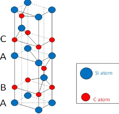
Silicon carbide crystal lattice is structured from closely stacked silicon and carbon
bilayers (also called Si-C double layers). Due to the variation of staking sequences of
atomic planes in one certain direction, silicon carbide has many crystal lattice structures
such as cubic, hexagonal and rhombohedral symmetry [27]. These different crystal lattice
structures of SiC are known as polytypes, and alphabetical letters are used to identify the
structure. For example, the letter „H‟ in 4H-SiC specifies that this polytype of SiC has
hexagonal symmetry. The integer number „4‟ represents the repetition number of bilayers
in the stacking sequence. Figure 1.1 shows the crystal structure of 4H-SiC. From the side
view, the staking sequence of SiC crystal shows a zig-zag pattern which terminates with a
silicon face on a surface and with carbon atoms on the opposing surface.
Due to the variation in the stacking sequence, different polytypes have
significantly different optical and electrical properties such as band-gap, drift velocity,
breakdown electric field strength, and the impurity ionization energies [27]-[30]. Among
different polytypes, 4H-SiC is usually preferred for electronic devices due to wide
bandgap energy and better charge transport properties, specifically high electron mobility
[31]-[33]. Low dielectric constant of 4H-SiC compared to Si and Ge helps to reduce the
detector capacitance for a given active detector volume, which in turn decreases the white
series noise component. The high threshold displacement energy indicates the radiation
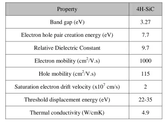
hardness of the material. Table 1.1 shows the properties of the polytype 4H-SiC that are
relevant for radiation detector fabrication.
Table 1.1 Properties of 4H-SiC
Property 4H-SiC
Band gap (eV) 3.27
Electron hole pair creation energy (eV) 7.7
Relative Dielectric Constant 9.7
Electron mobility (cm2/V.s) 1000
Hole mobility (cm2/V.s) 115
Saturation electron drift velocity (x107 cm/s) 2
Threshold displacement energy (eV) 22-35
Thermal conductivity (W/cmK) 4.9
G
ROWTH OF4H-S
ILICONC
ARBIDEM
ATERIAL1.4
High quality, defect-free semiconductor materials are needed to fabricate
recombination/generation centers leading to poor charge carrier lifetime-mobility which
reduces signal-to-noise ratio and thereby detector performance. Silicon carbide phase
diagram does not show a liquid phase, meaning SiC sublimes before it melts, therefore
SiC bulk crystals cannot be grown by solidification from melts. SiC bulk growth is
usually done by a method based on physical vapor transport (PVT), where a solid source
of silicon carbide is evaporated at high temperatures and the vapors then migrate and
crystallize on a monocrystalline SiC seed kept at a lower temperature [34]. In this method
of crystal growth, precise doping and uniformity cannot be controlled easily, and grown
crystals often suffer from microscopic crystallographic defects. Efforts have been made
to optimize the reactor design to better control thermal gradients inside the growth
chamber in order to increase wafer size and to reduce defect density [35]. At present,
3-inch diameter substrates are commercially available from multiple vendors [36].
However, bulk SiC available in the market still has relatively high defect densities and
impurity concentrations to be used for high performance detector device.
Hence, SiC device are fabricated not directly on the bulk SiC wafers, but on
epitaxial layers grown on top of the bulk SiC wafer. Epitaxial layer can be grown in a
more controlled and reproducible manner using techniques such as chemical vapor
deposition (CVD) yielding much higher quality SiC material than bulk SiC [37].
Epitaxial growth in a CVD system entails heating of the substrate in the reactor chamber
with flowing silicon and carbon containing gasses that decompose and deposit Si and C
in a well-ordered fashion onto the substrate to grow a high quality thin crystalline layer.
The n-type 4H-SiC epitaxial layers used to fabricate radiation detectors for our
(0001) substrates with a 4 - 8o offcut towards the ̅ ] direction. Epitaxial layers with
12 – 50 m thickness were grown by hot-wall CVD system using dichlorosilane
(SiH2Cl2, DCS) and propane (C3H8) as gas-phase precursors and hydrogen of 6 SLM as
the carrier gas. A dilution ratio of ~ 1000 was used and flow rates of precursors were
maintained to obtain a C/Si ratio of ~ 1.28. The growth temperature and pressure were
1550 °C and 80 - 120 torr, respectively. An in situ hydrogen etching of the substrate was
performed at 1550 °C for 5 – 20 min prior to growth. With horizontal hot-wall reactor, a
higher growth temperature (up to 2000 ˚C) could be reached with more efficient heating
of the substrate [38]. In this technique, the precursor gases are utilized more efficiently,
CHAPTER 2:
DETECTOR FABRICATION AND CHARACTERIZATION
O
VERVIEW2.1
4H-SiC detectors were fabricated on n-type (nitrogen-doped) 4H-SiC epitaxial
layer using Schottky barrier contact. Ni/4H-SiC radiation detector fabricated on 12 m
epitaxial layer was investigated for the first time in this study along with 20 m and 50
m epilayer based detectors. Details of detector fabrication and theory behind Schottky
contact are provided. Fabricated detectors were characterized using current-voltage (I-V)
and capacitance-voltage (C-V) measurements to determine electrical properties such as
leakage current, doping concentration, built-in potential, Schottky barrier height, and
ideality factor. A thermionic emission model was used to determine Schottky barrier
junction properties [39]. Built-in potential and barrier height specifies the amount of
current flow through the junction and the ideality factor specifies the spatial uniformity of
the barrier height across the diode surface [40]. These diode parameters are important
characteristics to predict device performance. Leakage current at applied reverse bias
across the detector is also an important property as the detector electronic noise increases
with leakage current thereby reducing the overall detector resolution [41]. Presence of
electrically active defects, which act as generation-recombination centers, can lead to
increased detector leakage current. The defects can also act as trap centers which may
lead to incomplete charge collection. Deep level transient spectroscopy (DLTS)
and to understand their impact on device performance. Low-leakage current and
low-defect bearing 4H-SiC detectors were then chosen for performance evaluation with
alpha-radiation source.
E
PITAXIAL4H-S
ILICONC
ARBIDED
ETECTORM
ATERIAL2.2
The n-type 4H-SiC epitaxial layers used to fabricate radiation detector for our
study were grown on 100 mm diameter wafers diced from highly nitrogen-doped 4H-SiC
(0001) substrates with a 4 - 8o offcut towards the ̅ ] direction. Epitaxial layers (12 –
50 m thick) were grown by hot-wall CVD system at a growth temperature of 1550 °C.
A picture of n-type 4H-SiC epitaxial layer wafer diced into 10×10 mm2 size pieces is
shown in Figure 2.1.
Figure 2.1 Photograph of an n-type 4H-SiC epitaxial layer wafer.
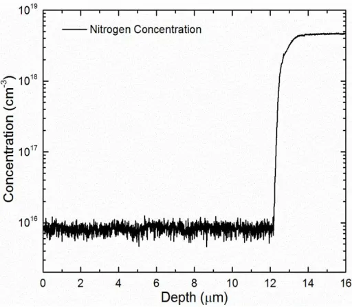
Nomarski optical microscopy and scanning electron microscopy (SEM) revealed
a micropipe defect density of less than 1 cm-2.Secondary ion mass spectrometry (SIMS)
measurement was performed to characterize the epilayer layer thickness and doping
observed due to the large nitrogen concentration difference in the epilayer and the highly
doped substrate. For this particular sample it was determined to be 12 μm thick with an
average nitrogen doping concentration of approximately 8 × 1015 cm-3.
Figure 2.2 SIMS measurement indicating a 4H-SiC epilayer thickness of 12 m and nitrogen doping concentration of ~ 8 × 1015cm-3.
N
I/4H-S
IC
S
CHOTTKYB
ARRIERD
ETECTORS
TRUCTURE2.3
Single-pixel, planar metal-semiconductor-metal (MSM) detector structure was
fabricated on n-type 4H-SiC epitaxial layers. In a planar detector structure, metal contacts
are placed on both sides of the detector material. The cross-sectional schematic of 8×8
mm2 detector is presented in Figure 2.3 showing 4H-SiC epilayer (active layer), 4H-SiC
buffer epilayer, and 4H-SiC bulk substrate with circular nickel (Ni) contact deposited on
the epilayer face (top contact) and larger square Ni bottom contact on the opposite side.
The circular Schottky barrier contact on the epilayer surface forms the „detector window‟
through which ionizing radiation is captured by the 4H-SiC epilayer. Therefore,
Figure 2.3 Cross-sectional view of Schottky barrier detector on 4H-SiC epitaxial layer.
(a) (b)
Figure 2.4 Energy band diagram of: (a) a metal and an n-type semiconductor before contact and (b) after Schottky contacts between metal and n-semiconductor [42].
In the fabricated detector structure, top nickel (Ni) contact forms a Schottky
contact with high-resistive n-type 4H-SiC epitaxial layer. Figure 2.4 shows energy band
diagram of an ideal Schottky contact between a metal and an n-type semiconductor at
thermal equilibrium. A metal-semiconductor contact is called Schottky contact when it
has a rectifying effect providing current conduction at forward bias (metal to
semiconductor) and a low saturation current at reverse bias (semiconductor to metal). The
rectifying effect of Schottky contact arises from the potential barrier present at metal-Vacuum level
Metal Semiconductor (n-type)
Vacuum level
semiconductor junction that restricts charge carrier movements. The potential barrier
height (e
Bo) for electron injection from the metal into the semiconductor conductionband (Ec) is known as the Schottky barrier and is the difference between the metal work
function ( and semiconductor electron affinity ():
2.1
where e is electron charge. Work function is the energy difference between the Fermi
level (EF) to the vacuum level and electron affinity () is the energy difference between
the semiconductor conduction band edge (Ec) and the vacuum level. In the ideal case, the
Schottky barrier height remains constant with respect to the polarity of the applied
voltage.
On the semiconductor side, the built-in potential barrier (Vbi) is the barrier for
electron flow from semiconductor conduction band into the metal and is given by:
22.2
where is semiconductor work function. Built-in potential Vbi increases or decreases
with applied voltage. In „forward‟ bias, where a positive voltage is applied to the metal in
respect to the semiconductor, Vbi is reduced so electrons can flow more easily from
semiconductor into metal.
Due to conduction band bending in a Schottky contact, an electric field develops
which sweeps free electrons from the vicinity of the contact interface and creates a
depletion region (also known as space charge region). The bands become flat at the edge
of the depletion region, and the electric field falls to zero at the edge which persists
throughout the semiconductor. The width of the depletion region, W, for a Schottky
increases with applied voltage at reverse bias. Width of the depletion region can be
expressed as:
√
2.3 where the dielectric constant of the semiconductor material, is the permittivity of
vacuum, is the electronic charge (1.6 × 10⁻¹⁹ C) and is the effective doping
concentration and Vbi is the built-in potential.
The thermally annealed bottom Ni-contact forms an Ohmic contact with the very
low-resistive bulk 4H-SiC substrate. The energy band diagram of an ideal Ohmic contact
in Figure 2.5 shows that there is no potential barrier to block electron flow, hence
providing conduction in both directions.
Figure 2.5 Energy band diagram of an ideal Ohmic contact between metal and n-type semiconductor [42].
D
ETECTORF
ABRICATION2.4
Prior to detector fabrication, the SiC wafer was thoroughly cleaned using a
modified Radio Corporation of America (RCA) cleaning process. The cleaning process
starts with removal of organic contaminants (dust particles, grease, etc.) from the wafer
surface using organic solvents (trichloroethylene, acetone, and methanol) at their
respective boiling temperatures. Any organic residue left by the first step is then removed Semiconductor
using first ammonium hydroxide (NH4OH) solutions with hydrogen peroxide
(H2O:H2O2:NH4OH = 5:1:1) and then piranha solution (H2SO4:H2O2 = 1:1). Finally,
oxide layers are etched with hydrofluoric acid (HF) followed by a Type 1 DI water rinse
prior to metal contact deposition.
To form back Ohmic contact, large Ni contact (~ 6 × 6 mm2) of 100 nm in
thickness was deposited on the bulk side (C-face) of the 8 × 8 mm2 4H-SiC wafer using a
Quorum Q150T DC sputtering and a shadow mask. This was followed by rapid thermal
annealing (RTA) at 950°C for 2 minutes in high-purity argon (Ar).
Photolithography was then performed on the epilayer side of the sample to pattern
a 3.8 mm diameter circular window for Schottky contact formation. The sample was
coated with Microposit SC1813 positive photoresist. A Karl Suss MA-6 Mask Aligner
was used to expose a 3.8 mm diameter area centered on the sample by a quartz mask. The
sample was then submersed in Microposit MF-319 developer for 1 minute followed by
Type1 DI water rinse and drying by compressed N2 gas. A Ni Schottky contact (3.8 mm
diameter circular shape) with an area of ~ 11.34 mm2 and thickness of ~ 10 nm was
deposited on top of the epitaxial layers (Si-face) through the shadow mask using a
Quorum model Q150T sputtering unit followed by a lift-off process.
After fabrication, the detector was then mounted on a printed circuit board (PCB)
designed and fabricated in our laboratory and wire bonded for proper electrical
connection. The wire-bonding was done using very thin (25 m) gold wire to ensure less
scattering and obscuration of the alpha particles from the wire-bond region. The PCBs
configuration for stable electrical connections. A photograph (top view) of a fabricated
detector is shown in Figure 2.6.
Figure 2.6 Photograph of a 4H-SiC epitaxial Schottky barrier detector with circular nickel top contact mounted on a PCB. This PCB is designed and fabricated in our laboratory.
C
URRENT-V
OLTAGEM
EASUREMENT2.5
Current-voltage (I-V) measurements on the fabricated Schottky barrier 4H-SiC
epitaxial detectors were carried out at room temperature (300 K) using a Keithley 237
HV SMU. I-V characterizations were performed by measuring the current flowing
through the 4H-SiC detector at various forward as well as reverse voltage bias applied
across the detector. The forward-biased response was used to study the behavior of the
Schottky contacts in terms of barrier height and the diode ideality factor applying the
thermionic emission model [40], [24-25]. The reverse I-V characteristics were used to
determine the leakage current under operating conditions. As per a thermionic emission
model, the voltage dependent junction current in a Schottky contact can be given by:
( ) ( ( ) ) 2.4
where is the Richardson‟s constant taken to be 146 A·cm-2K-2 for 4H-SiC [43], A is
the diode area, T is the absolute temperature,
e
is the electron charge (1.6 × 10⁻¹⁹ C),k
B isapplied voltage, and
n
is the diode ideality factor. Using logarithm, the Equation 2.4could be written as:
2.5
where is the saturation current, ( ) and . Therefore,
using current measurements at varying applied voltage and then plotting log(I) versus
applied voltage bias, saturation current can be obtained from the intercept and the
ideality factor „n‟ could be measured from the slope using following equation:
⁄ 2.6
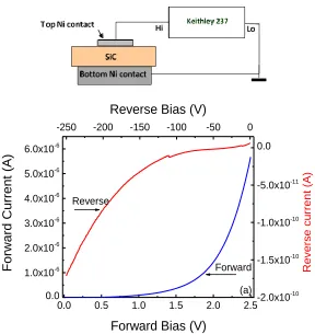
Figure 2.7, a typical I-V characteristic, shows the variation of forward and reverse
current as a function of applied bias voltage across the n-type 4H-SiC epitaxial Schottky
detector with Ni-contact. Schottky behavior of the device is clearly visible from this I-V
characteristic measurement at room temperature. The reverse bias leakage current at
room temperature was found to be ~ 0.18 nA at a bias voltage of -250 V. A logarithmic
plot of voltage-dependent junction current is shown in Figure 2.8 for 12 m n-type
4H-SiC epitaxial Schottky detector with Ni-contact. A Schottky barrier height of 1.10 eV was
determined by applying the thermionic emission model as discussed in Equation 2.5. The
diode ideality factor of 1.29 was measured from the slope using Equation 2.6. An ideality
factor greater than unity, indicates inhomogeneity of the Schottky barrier height across
the metal contact, most probably due to the presence of generation-recombination centers
or trap centers (defect centers) on the detector surface [7], [44]. Lower barrier height also
occurs due to the presence of defects in the epilayer arising from the growth process and
Figure 2.7 Variation of junction current for n-type 20 m 4H-SiC epitaxial/Ni Schottky detector with forward and reverse applied bias at room temperature; schematic of the
electrical circuit for I-V measurements is shown at top
Figure 2.8 I-V characteristic with current on logarithmic scale showing the rectifying behavior of the Ni Schottky contact formed on the 12 m 4H-SiC epilayer.
0.0 0.5 1.0 1.5 2.0 2.5
0.0 1.0x10⁻⁶ 2.0x10⁻⁶ 3.0x10⁻⁶ 4.0x10⁻⁶ 5.0x10⁻⁶ 6.0x10⁻⁶
0 20 40 60 80 100
0 50 100 150 200 250 300 350 400 450 Forwa rd Cu rren t (A)
Forward Bias (V)
-250 -200 -150 -100 -50 0
-2.0x10⁻¹⁰ -1.5x10⁻¹⁰ -1.0x10⁻¹⁰ -5.0x10⁻¹¹ 0.0 (a) Re verse Cu rren t (A)
Reverse Bias (V)
Reverse
Forward
0 20 40 60 80 100 40 60 80 100 120 140 160 Capacita nce (p F) Bias (V) 1/C
2 (nF 2 )
Experimental Data Linear Fit
Bias Voltage (V)
C
APACITANCE-V
OLTAGEM
EASUREMENT2.6
Capacitance-voltage (C-V) measurements at room temperature under dark
condition were carried out at a frequency of 1 MHz. The C-V measurements were
performed to determine effective carrier concentration and built in potential for n-type
4H-SiC epitaxial Schottky detectors. The junction capacitance of Schottky barrier contact
depends on the depletion region width which is a function of applied voltage (V) and
effective doping concentration ( ) as expressed in Equation 2.3. Using that equation,
the following relationship can be derived between junction capacitance (C), effective
carrier concentration ( ) and built-in potential ( ):
(
)
⁄ 2.7
where A is the area of the diode, is the product of the relative permittivity in 4H-SiC
and free space, and e is charge of an electron. The above equation could be rewritten as
below:
2.8
Applying the linear fit described in Equation 2.8, when 1/C2 is plotted against applied
voltage bias, V, built-in voltage ( could be estimated, from the intercept, and the
effective doping concentration (Neff) could be determined from the slope using the
following formula:
2.9
Once doping concentration and built-in voltage is determined, the barrier-height ( can
2.10
where NC is the effective density of states in the conduction band of 4H-SiC and is taken
equal to 1.6×1019 cm-3 [30].
Figure 2.9 shows a 1/C2 vs V plot, also known as Mott-Schottky plot, obtained for
the12 m n-type 4H-SiC epitaxial Schottky detector at 300 K. From the slope of the
straight line Neffwas calculated using Equation 2.9 and found to be 1.03 × 1015 cm-3 with
the built-in potential Vbi determined to be 1.91 V where the extrapolated line intersects
the voltage axis. The higher built-in potential can be explained by the presence of a thin
oxide layer at the metal-semiconductor interface which introduces an additional small
series capacitance. Since the slope of the line in Figure 2.9 depends on the effective
doping concentration, the slope would remain the same in presence of a thin oxide layer
while the intercept with the voltage axis would be shifted to a higher value [45], [46] –
[49]. The barrier height calculated from the C-V measurements using Equation 2.10 is
1.38 eV, which is slightly higher than the value of 1.10 eV obtained from the forward I-V
characteristics. This is due to the fact that while the barrier-height obtained from forward
I-V characteristics is affected by low Schottky barrier height locations in an
inhomogeneous diode, the barrier height determined from C-V characteristic gives an
average value for the whole diode [29], [50]. The larger value of barrier height calculated
from the C-V measurements further confirms the inhomogeneity of the surface barrier
Figure 2.9 Mott-Schottky plot (1/C2 vs. V plot) of Ni/4H-SiC Schottky barrier detector fabricated on 12 m thick n-type 4H-SiC epitaxial layer. Inset shows original C-V
characteristic at 300 K.
D
EFECTS
TUDY BYD
EEPL
EVELT
RANSIENTS
PECTROSCOPY2.7
Intrinsic defects, such as grain boundaries and dislocations, impurity related point
defects or complexes have been reported in as-grown SiC epilayers [18], [50] - [53].
Many of these defects act as trap or recombination/generation centers and can lead to
increased detector leakage current (thereby noise), loss of charge carriers and/or
incomplete charge collection. The current-voltage and capacitance-voltage measurement
of the fabricated Schottky barrier detector on 4H-SiC epitaxial layer showed evidence of
non-uniform barrier height due to the presence of defect centers. Therefore, it is
important to identify the electrically active defects in the epilayer and evaluate their role
in affecting the ultimate detector performance.
The presence of deep level defects was investigated by deep level transient
spectroscopy (DLTS) in a temperature range from 80 K to 800 K. DLTS measures the
carriers from the defects existing in the space charge region. A capacitance-DLTS
(C-DLTS) spectrum is generated from the temperature dependent capacitance transients
followed by a saturated trap filling pulse applied to a semiconductor junction. By
analyzing the capacitance transients, the defect activation energies (∆E), which is the
energy separation between the trap level and the conduction band, capture cross-sections
(σn,), which determines if the defects may act as a trap or recombination/generation
center, and defect concentration (Nt), which provides the extent of defect on device
performance, can be determined [54], [55].
In C-DLTS mode, the thermally activated emission rate, , can be expressed as:
〈 〉 ⁄ ⁄ 2.11
where σn is the carrier capture cross section, 〈Vth〉 is the mean thermal velocity, NC is the
effective density of states, g is the degeneracy of the trap level and was considered to be
equal to 1, ∆E the energy separation between the trap level and the carrier band, is the
Boltzmann constant (8.62 × 10⁻⁵ eV/K), and T is the absolute temperature. The emission
rate is related to the capacitance transient by the following relationship:
2.12
where C0 is the junction capacitance at steady-state reverse bias voltage, ∆C is the
difference in capacitance change measured within the rate window. The trap
concentration Nt can be calculated using the following expression:
where ∆C(0) is the difference in capacitance change between the two edges of the filling
pulse and Nd is doping concentration. The peak position in DLTS spectroscopy depends
on the rate window, τ, which is defined by an initial delay set for the emission rate
calculations following the termination of the filling pulse:
⁄ 2.14
For defect characterization in 4H-SiC epitaxial Schottky barrier detector, a SULA
DDS-12 modular DLTS system was used in a capacitance mode. The DLTS system is
comprised of a pulse generator, a capacitance meter, a correlator module, a Janis VPF
800 LN2 cryostat controlled by a Lakeshore LS335 temperature controller, and a PC
based data acquisition and analysis software. The correlator module uses a modified
double boxcar signal averaging algorithm and automatically removes DC background
from the capacitance signals and measures the capacitance transient in a given rate
window.
The DLTS measurements were carried out using a temperature range of 80 - 800
K at a heating rate of 0.05 Ks-1 and a steady-state reverse bias of -2 V pulsed to 0 V to fill
carrier traps present within the depletion width. DLTS software allows the collection of
four DLTS spectra simultaneously with four independent correlator delay settings in a
single temperature scan as shown in Figure 2.10. Five distinct negative peaks appeared at
different temperatures corresponding to different defect levels indicating majority carrier
(electron) traps. The activation energy (∆E), which corresponds to the energy difference
between the trap level and the conduction band, was calculated for each defect level from
the Arrhenius plots ⁄ ⁄ shown in Figure 2.11. The defect parameters
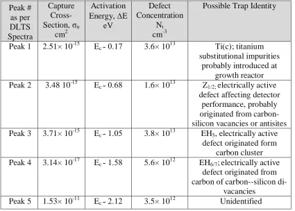
the DLTS scans using the Equations 2.11 - 2.13 and summarized in Table 2.1. The
observed defect level was then compared with the literature values, if available, reported
by other researchers.
Figure 2.10 DLTS spectra obtained using n-type Ni/4H-SiC epitaxial detector in the temperature range of: (a) 80 to 140 K using a smaller set of initial delays, and
(b) 150 to 800 K using a larger set of initial delays.
Figure 2.11 Arrhenius plot for all the peaks obtained from the DLTS scans.
The activation energy for trap levels in Peak #1 was found to be Ec - 0.17 eV,
which means this defect level is located at 0.17 eV below the conduction band minimum
Peak # 3 Peak # 2
Peak # 4 Peak # 5
Temperature (K)
Peak # 1
(a) (b)
(Ec). This is a shallow level defect, and from the available literature, can be identified as
titanium (Ti) substitutional impurities in the Si sites. Similar defect levels at Ec - (0.160 ±
0.010) eV were reported from DLTS studies of Ti+ implanted 4H-SiC which were
attributed to the ionized titanium acceptor Ti3+ (3d1) residing at hexagonal and cubic Si
lattice [52], [56]. The presence of Ti impurity is likely introduced during the growth
process from the Ti parts in the growth reactor. Other research groups also assigned
defect level located at Ec - 0.16 eV as Ti electron trap [53], and trap level located at Ec -
0.17 eV as chromium or titanium impurities (acceptor like) in hexagonal position [51].
Table 2.1 Defect parameters obtained from the DLTS measurements
Peak # as per DLTS Spectra Capture Cross-Section,σn
cm2
Activation
Energy, E
eV
Defect Concentration
Nt cm-3
Possible Trap Identity
Peak 1 2.51× 10⁻¹⁵ Ec ˗ 0.17 3.6× 10¹³ Ti(c); titanium
substitutional impurities probably introduced at
growth reactor
Peak 2 3.48 10-15 Ec ˗ 0.68 1.6× 10¹³ Z1/2; electrically active
defect affecting detector performance, probably originated from carbon-silicon vacancies or antisites
Peak 3 3.71× 10⁻¹⁵ Ec ˗ 1.05 3.8× 10¹³ EH5, electrically active
defect originated form carbon cluster
Peak 4 3.14× 10⁻¹⁷ Ec ˗ 1.58 5.6× 10¹² EH6/7;electrically active
defect originated from carbon of carbon--silicon
di-vacancies
Peak 5 1.53× 10⁻¹¹ Ec ˗ 2.12 3.5× 10¹² Unidentified
The position of defect level associated with Peak #2 was found at 0.68 eV below
level often designated as Z1/2 in n-type 4H-SiC [55]-[60]. Z1/2 center is reported to be an
electrically active defect responsible for the reduction of carrier lifetime which is
detrimental to detector performance [52], [60]. The exact microscopic structure is still
unknown but most likely it is originated from carbon related vacancies, silicon and
carbon vacancy complexes (VSi+VC) or antisite complexes (SiC+CSi) [53], [55], [58].
The peak #3 was related to a defect level located at 1.06 eV below the conduction
band edge. Similar defect levels at Ec-1.03 eV and at Ec-1.07 eV were observed by other
researchers [61], [62]. This defect level designated as EH5 has been found in ion
irradiated 4H-SiC and has been attributed to a carbon cluster [58].
The position of peak #4 in the bandgap was calculated to be at Ec-1.58 eV. The
nearest match for this defect level reported in literature was at Ec-1.6 eV and at Ec-1.55
eV, which were designated as EH6/7 defect level and related it to carbon vacancies (VC) or
carbon-silicon di-vacancies [63], [64]. Further investigation is in progress to clearly
resolve peaks #3 and #4. Several groups have tried various methods to resolve the level
termed EH6/7 and have reported activation energies ranging from 1.35 eV to 1.58 eV for
resolved EH6 and EH7 levels [52], [57], [65]-[67]
The peak #5 was related to a defect level located at 2.12 eV below the conduction
band edge, and remains unidentified. No similar defect level has been reported in the
literature to best of our knowledge. Further investigations are in progress.
A defect level in n-type 4H-SiC epitaxial located at 1.32 eV below the conduction
band edge, which was observed by our research group and others, was not present in this
particular sample [18], [50], [58] [61]. This defect was assigned to be defect center Ci1 in
S
UMMARY OFN
I/4H-S
IC
D
ETECTORC
HARACTERIZATION2.8
A total of four different Ni/4H-SiC detectors were investigated that were
fabricated on 12 m or 20 m thick n-type 4H-SiC epitaxial layer using the fabrication
process described in this chapter. These detectors are listed in Table 2.2. Among these
detectors, 12 m Ni/4H-SiC epilayer were investigated for the first time as radiation
detector [68]. Detector 2AS1a was fabricated using relatively higher quality n-type
4H-SiC and used for front-end readout electronics noise analysis as described in Chapter 3.
An additional two 20 m detectors provided baseline data for further study with edge
termination described in Chapter 4. Being fabricated from the same substrate, they could
also be used to demonstrate detector reproducibility. Applying different characterization
techniques described in above sections of this chapter, these detectors were studied for
their Schottky barrier properties, leakage current, doping concentration, and defect
concentration. The results of this analysis are summarized in Table 2.3.
Table 2.2 Baseline Ni/4H-SiC epitaxial detectors
Detector ID Epilayer
Thickness
Purpose Served
1AS1 12 m Investigated for the first time to use as radiation detector
2AS1a 20 m Fabricated with higher quality epitaxial layer and used for
electronic noise analysis
2AS22x 20 m Detector used to assess edge termination with SiO2
Table 2.3 Summary of characterization for baseline Ni/4H-SiC epitaxial detectors Detector ID Leakage Current at -200V (nA) Barrier Height (eV) Diode Ideality Factor Doping Concentration (×1014 cm-3)
Density of Z1/2 Defect
(×1014 cm-3)
Capture Cross-section of Z1/2 Defect
(×10-16 cm2)
1AS1 0.181 1.10 1.29 10.3 1.58 9.12
2AS1a 0.12 1.39 1.18 1.8 4.16 5.04
2AS22x 4.72 1.01 1.35 2.86 1.6 34.8
2AS30x 4.52 1.00 1.24 2.42 Not tested Not tested
1
measured at -250 V for detector 1AS1
C
ONCLUSION2.9
Schottky barrier radiation detectors were fabricated on n-type 4H-SiC epitaxial
layers grown on a 4˚ off-axis highly doped 4H-SiC substrate (0001). Planar single-pixel
MSM detector structure with Ni Schottky top contact (detection window) was used.
Schottky barrier properties were characterized through current-voltage (I-V) and
capacitance-voltage (C-V) measurements. The room temperature I-V measurements
revealed a very low leakage current ranging from a few to a fraction of nA at 200 V
reverse bias. The barrier height for Ni/4H-SiC Schottky contact was found to be in a
range of 1 to 1.4 eV by forward I-V measurement. From a Mott-Schottky plot of the C-V
measurements, the effective carrier concentration was calculated and found to be in a
range of 1.8 - 10 × 1014 cm-3. Using a thermionic emission model, the diode ideality
factor was determined to be ≥1.18, which is higher than „unity‟ indicating the presence of
deep levels as traps or recombination centers in the detector volume. Capacitance-mode
deep level transient spectroscopy (DLTS) measurements were carried out to investigate
the defect levels in the detector active region. DLTS revealed the presence of a shallow
level, and two deep level defects assigned as EH5, and EH6/7 which are related to carbon
or carbon-silicon di-vacancies. The concentration and capture cross-section of Z1/2, which
is the most detrimental defects to detector performance, were determined to be ≥1.6 ×
1014 cm-3 and ≥ 5 × 10-16 cm2, respectively. An unidentified deep electron trap located at
2.12 eV below the conduction band minimum was observed, but the nature and origin of
the defect is unknown. Thus, the electrical characterization along with defect
characterization of the fabricated n-type 4H-SiC epitaxial layer detector provided useful
information and serves as a quality control tool in selecting detectors that would be
CHAPTER 3:
PULSE-HEIGHT SPECTROSCOPY AND NOISE
ANALYSIS OF FRONT-END READOUT ELECTRONICS
O
VERVIEW3.1
The response of the detectors to alpha particles was evaluated by irradiating the
detector with 0.1 Ci 241 Am alpha source which provides low-energy gamma-rays at
59.6 keV or alpha particles at 5.486 MeV and by recording the pulse-height spectrum
produced from detector measurements. Front-end readout electronics consisted of
preamplifiers which converts charge signal generated by incident alpha particles to a
voltage signal, shaping amplifier that filters noise, and multi-channel analyzers (MCA)
which converts analog signals into digital information as pulse-height spectrum. Detector
performance was evaluated in terms of energy resolution of the detection peak obtained
by PHS. The energy resolution was calculated at full width at half maximum (FWHM) of
the alpha energy peak using Gaussian peak fitting function. The charge collection
efficiency (CCE) is the ratio of the output energy observed by the detector to the actual
incident energy of the alpha particles (5.48 MeV), and was calculated as a function of
reverse bias using a drift-diffusion charge transport model. Finally, electronic noise
analysis of front-end readout system was carried out in terms of equivalent noise charge
(ENC) in order to study the contribution of white series noise, pink noise ( parallel and