Implementation of 32 Bit Fixed Point Arithmetic Logic
Unit (ALU), on FPGA using VHDL
Neelesh Kumar Kachhwaha
1, Prof.Sunil Shah
2 1Tech (VLSI Design) Gyan Ganga Institute of Technology and Sciences Jabalpur, MP (India)
2
ept. of ECE Gyan Ganga Institute of Technology and Sciences Jabalpur, MP (India)
ABSTRACT
Reconfigurable systems offer a solution to solve complex problems by combining the speed of hardware with the
flexibility of software to improve performance and system performance. Past three decades have seen the
introduction of the technology that has radically changed the way one analyses and controls the world around
them. Exploiting computational precision can improve performance significantly without losing accuracy in
many applications. To enable this, we propose an innovative arithmetic logic unit (ALU) architecture that
supports true dynamic precision operations on the fly. As the operations become more complex the ALU also
become more complex, more expensive and takes up more space in the CPU hence power consumption is a
major issue. The VHDL coded synthesizable RTL code of the Fixed Point Arithmetic core has a complexity. We
verified the functions of the Fixed Point Arithmetic by a simulation with a single instruction test as the first step
and then implemented the Fixed Point Arithmetic with the FPGA. Nowadays to handle the more challenges and
complex task the demand of improving ability of a processor is increasing day by day which resulted in the more
numbers of components fabricated on a single chip according to the Moore Law.
I.INTRODUCTION
objective of the project is to have a working ALU that performs different arithmetic and logic functions for all possible combinations of the inputs. The speed of ALU was not an issue and we wanted it to run at low power. ALU is capable of calculating the results of a wide variety of basic arithmetical and logical computations. The ALU takes as input the data to be operated on (called operands) and a code from the control unit indicating which operation to perform. The output is the result of the computation. The ALU implemented will perform the following operations:
Arithmetic operations(addition, subtraction, increment, decrement, transfer). Logic operations (AND, NOT, OR, NAND, NOR, EX-OR, EX-NOR).
A digital system can be represented at different levels of abstraction [1]. This keeps the description and design of complex systems manageable. The highest level of abstraction is the behavioral level that describes a system in terms of what it does (or how it behaves) rather than in terms of its components and interconnection between them. Here the 32- bit ALU is implemented by using the behavioral modeling style to describe how the operation of ALU is being processed. This is accomplished by using a hardware description language VHDL. The behavioral style makes use of a process statement. A process statement is the main construct in behavioral modeling that allows using sequential statements to describe the behavior of a system over time. Process is declared within architecture and is a concurrent statement. However, the statements inside a process are executed sequentially. A process do read and write signals and values of the interface (input and output) ports to communicate with the rest of the architecture just like other concurrent statements. In this paper, section II deals with modeling style, block diagram, specifications and VHDL code for 32-bit ALU, section III presents simulation results and discussion and section IV follows conclusions.
II.MIPS INSTRUCTION SET ARCHITECTURE
The instruction set can be categorized under three classifications in the MIPS ISA, these are: Register type (R),
Immediate type (I) and Jump type (J).
Each instruction starts with a 6-Bit Op-code. Alongside these op-code, Register type (R) define 3 (three) registers, Immediate type (I) instructions define2 (two) registers and a 16Bitevaluation; Jump type (J) instructions have an op-code of 26Bit.
The following table demonstrates the three formats used for the MIPS core instruction set architecture.
I-
Register (R) Type Instructions:
Register (R) Type Instructions
Succeeding 5-bits are the shift sum which betokens the number of bits that are to be moved. The final 6-bits represent the function field points to the function which are to be executed on the registers.
II-
Immediate (I) Type Instructions:
Immediate (I) type instructions are demonstrated in Fig.3. The four fields portrayed in this type of arrangement represent - the Op-code, which is of 6-bitthat is utilized to select the Instruction type, storing of data is done in the Source Register and Target Registers which are Rs and Rt respectively. Each are of 5-Bit. The final 16-bit Address/Immediate Value field wielding prompt data.
Fig. Data Path for Immediate (I) type instructions.
III-
Jump (J) type Instructions (Branch Format)
The instruction format shown in Fig. is that of Branch Type [1]. The two fields illustrated in this arrangement type are the Op-code which is of 6-bit, utilized to choose the kind of instruction organization and Ending or Target address of 26-bit, utilized to determine where the address has to be branched.
The data path for Jump (J) type instruction is illustrated in Fig. The figure demonstrates that a 32-bit jump (J) address is obtained when the last 4 bits of PC + 4 are attached to the shift left by 2 values of a 26-bit instruction captured out from MEM. In addition, it jumps to the destination by omitting any alternate instruction.
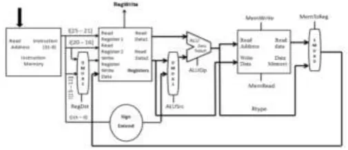
III.MIPS ARCHITECTURE
The accompanying outline demonstrates the fundamental architecture of a MIPS-based framework:
Microprocessor without Interlocked Pipeline Stages (MIPS) is a RISC (Reduced Instruction Set Computing) architecture. Pipelined MIPS has five stages which are IF, ID, EX, MEM and WB. Pipelining means several operations in single data path at the same instant. Pipelining is used to enhance the capabilities of the RISC processor which is the reason for its utilization in this type of computer architecture. A multi-cycle CPU comprises of countless tasks. So if one task occurs, rather than waiting for the process to finish, at the same time another task is initiated in the same data path simultaneously without interfering with the previous task. The processes are thus divided into different pipelined stages. Following every clock a new operation is instigated in the pipeline stage to which the process is being fed to. The triggering is done without causing any interruptions to the past process. This makes simultaneous utilization of all stages in the data path possible. This thusly can increment the throughput of MIPS.
5 Stage MIPS Architecture (Pipelined)
3.1 Instruction Fetch (IF)
The command relayed to the Program Counter (PC) to fetch the instruction from the cache memory is what instigates the primary pipelining operation of the IF stage. The storage of PC and Instruction for the successive clock cycle is done in the IF/ID pipelined register as RAM (Random Access Memory)
IF Stage representation
IF stage for the most part relies on upon PC‟s represent value. On the basis of the PC value the processor gets the instructions from the cache and followed by which the Program Counter value is incremented by 1. Thus, the IF/ID register receives this information followed by which the information is relayed to the decoder unit. The Instruction Fetch (IF) stage operation has been represented in Fig.
3.2 Instruction Decoder (ID)
The Op-code is relayed to the decoder unit at the instant when the instruction is obtained from the IF stage. Instruction Decoder ID stage directs the controlling command to the various units of the MIPS processor examining the Op-code of the instructions. Thus the procurement of data from the MIPS registers is carried out by the Read register. The Branch unit is likewise incorporated into Instruction Decoder (ID) stage. The Input data of ID stage is received from IF stage as shown in Fig. 8.This decoding stage includes four different instructions: Register (R) type, Immediate (I)type, Jump (J) type and Input/Output (I/O) type instructions. Depending upon these instructions the function will be performed utilizing above mentioned formats. Fig.10. indicates Instruction Decode (ID) stage operation.
Instruction Decoder (ID)
3.3 Execute (EX)
particular, EX/MEM pipelined register receives the result upon the execution of specific instructions (i.e. FP ALU). Execute stage representation is shown in Fig.
3.4 Memory Access & Input/Output (MEM)
The storing and loading of values along with inputting and outputting data from the processor is the primary function of the memory access (MEM) stage. The outcome will be dispatched to the WB stage in a scenario where
the instruction is neither memory nor IO instruction. After the result is figured the
primary function is to store the data values in the destination register. The Memory Access
(MEM) stage operation is demonstrated in Figure.
3.5 Write Back (WB)
As per Figure the Write-Back (WB) operation is the final stage of the RISC based MIPS architecture which composes the result, store information and input data from and to the register files.
Writing the data that has been fetched from the MIPS register to the target register is the main aim of this stage.
IV.PIPELINED ARCHITECTURE
The five pipelined stages can be described as follows: Fetch: the processor reads the instruction from instruction memory.
Decode: processor reads the source operands from the register file and decodes
The instruction to produce the control signal Execute: performs the computation with the ALU. Memory: processor reads from or writes into the data memory.
Write back: processor writes the result to the register file when applicable.
Each instruction is thus broken up into a series of steps, and several steps of different instructions are executed simultaneously, improving the throughput significantly.
4.1 Pipelined Data path
The single-cycle processor is converted into the pipelined processor by adding registers. Figure shows the pipelined data path formed by inserting four pipeline registers to separate the data path into five stages. In pipelining, all signals associated with a particular instruction must advance through the pipeline in unison. We observe that the write back to the register file gets the data from Result W and hence, the address signal Write Reg has to be pipelined along through the memory to remain in sync.
Pipelined Control Unit Control signals for pipelined processor are same as the single-cycle processor and hence, control unit is the same. The op-code and function fields of the instruction are examined in the decode stage by the control unit to produce the control signals.
Pipelined processor with control.
They must be pipelined along with the data to remain synchronized with instruction. Figure shows the control and data unit for pipelined architecture.
All the programs running on the MIPS use the same instruction set. Instructions indicate both the operations to perform and the operands to use. The operands may be read from memory, from registers, or from the instruction itself. Representation of the instructions in a symbolic format is called assembly language. Instruction operates on operands and these operands can be stored in registers, memory, or they can be constants stored in the instruction itself. Registers are used for quick access to operand but they hold relatively a small amount of data. Additional data can be stored in a large data memory, which can be relatively slow. MIPS is a 32-bit architecture because operands are 32-bit data.
V.SIMULATIONS AND RESULTS
Instruction Fetch (IF) unit, memory unit (MEM) and execution unit (EX). In this process, the program counter (PC) is utilized while fetching the Op-code from Instruction Fetch (IF) stage and sending the code to Instruction Decode (ID) stage. Instruction Fetch (IF) stage receives the Op-code from the ID unit which is then sent for execution in the EX stage. The instruction configuration chosen is dependent on the Op-code. The execution of the instruction in the EX stage occurs in accordance with the assigned Op-code. Storage of Op-code to the memory and fetching it from the memory is the primary task of the memory unit.
In this paper we are looking into the ASIP performance results, Xilinx ISE and XST Synthesis tools. The register transfer level (RTL) description of the ASIP micro-architecture is designed and simulated in VHDL using Xilinx ISE design suit and basic functionality is verified using the assembly codes and results are verified.
Low Power Technique:
There are several different RTL and gate-level design strategies for reducing power. In the present work, Clock Gating design is used for reducing dynamic power. In this method, clock is applied to only the modules that are working at that instant [11]. Clock gating is a dynamic power reduction method in which the clock signals are stopped for selected registers banks during the time when the stored logic values are not changing. The clock pulse for low power technique is shown in Fig. 3. The input to low power unit is global clock and its output is gated clock, since the module will block the main clock in the following conditions.
When instruction is halt.
When there is a continuous Nop operation. When program counter fails to increment.
Divide module of FP 32 bit ALU Resp module of FP 32 bit ALU
FP 32 bit basic structure of ALU
VI.CONCLUSION AND FUTURE WORK
This paper demonstrates quad fixed point arithmetic processor with 32 bit data processing capability is
implemented. Quad Fixed Point 32-bit Arithmetic Core implements a full customizable arithmetic core using the Quad Fixed Point 32-bit. Available arithmetic operations are easily configured by an generic flag. Benefits are much less area requirements lesser pipeline depth and higher speed compared to an FPU at the cost that the number range is limited from +- 2^(-24) to 2^29.
employed for addition, subtraction, multiplication. Performance of Design are compared with fixed-point other simulation results. Fixed-point ALU using Newton-Raphson division and block wise analytical inversion algorithms achieve precession error in the range 10-5. The design is further synthesized and results indicate the max frequency of 101 MHz. Load word (lw) instruction is used to fetch the data into register file, which is the slowest instruction. Loading the back-to-back data from concurrent memory locations into the register file using a single new instruction is another suggested scope for improvement.
This research paper outlines a 32-bit Microprocessor without Interlocked Pipeline Stages (MIPS) based RISC processor is executed effectively with pipelining. In a five stage pipelining system the execution of each direction occurs in a single clock cycle. This design demonstrates the usage of MIPS based CPU equipped for taking care of different Register type, Jump type and immediate type of instructions and each of these classifications has a diverse configuration.
REFERENCES
[1.] Pranjali S. Kelgaonkar, Prof. ShilpaKodgire, “Design of 32 Bit MIPS RISC Processor Based on Soc”, International Journal of Latest Trends in Engineering and Technology (IJLTET), January 2016.
[2.] Ramandeep Kaur, Anuj, “8 Bit RISC Procesor Using Verilog HDL”, Int. Journal if Engineering Research and Applications, March 2014.
[3.] PreetamBhosle, Hari Krishna Moorth, “FPGA Implementation of low power pipeline 32-bit RISC Proessor”, International Journal of Innovative Technology and Exploring Engineering (IJITEE), August 2014. [4.] Gautham P, Parthasarathy R, Karthi, Balasubramanian, “Low Power Pipelined MIPS Processor Design”, in the proceedings of the 2009, 12th international symposium, 2009 pp. 462-465.
[5.] Neenu Joseph, Sabarinath S, “FPGA based Implementation of High Performance Architectural level Low Power 32-bit RISC Core”, 2009 IEEE.
[6.] “Computer Organization and Design- the hardware/software interface”, 3rd edition by David A. Patterson and John L. Hennessy, pp. 370-412.
[7.] Mrs. RupaliBalpande, Mrs. RashmiKeote, “Design of FPGA based Instruction Fetch & Decode Module of 32-bit RISC (MIPS) Processor”, International Conference on Communication Systems and Network
Technologies, 978-0-7695-4437-3/11, 2011 IEEE.
[8.] Harpreet Kaur, Nitika Gulati, “Pipelined MIPS with Improved Datapath”, IJERA, Vol. 3, Issue 1, January –
February 2013, pp. 762-765.
[9.] Accuracy-aware processor customisation for fixed-point arithmetic Shervin Vakili ✉, J.M. Pierre Langlois, Guy Bois IET Comput. Digit. Tech., 2016, Vol. 10, Iss. 1, pp. 1–11
[10.] J. Kurzak and J. Dongarra, "Implementation of mixed precision in solving systems of linear equations on the Cell processor: Research Articles," Concurr. Comput. : Pract. Exper., vol. 19, pp. 1371-1385, 2007.
[12.] J. Lee and G. D. Peterson, "Iterative Refinement on FPGAs,"in Application Accelerators in High-Performance Computing (SAAHPC), 2011 Symposium on, 2011, pp. 8-13.
[13.] A. R. Lopes, A. Shahzad, G. A. Constantinides, and E. C.Kerrigan, "More flops or more precision? Accuracy parameterizable linear equation solvers for model predictive control," in IEEE Symposium on Field Programmable Custom Computing Machines, Napa, California, 2009.
[14.] J. Sun, G. D. Peterson, and O. O. Storaasli, "High-Performance Mixed-Precision Linear Solver for FPGAs,"IEEE Trans. Comput., vol. 57, pp. 1614-1623, 2008.
[15.] Yiannacouras, P., Steffan, J.G., Rose, J.: „Exploration and customization of FPGA-based soft processors‟, IEEE Trans. Comput.-Aided Design Int. Circuits Syst., 2007, 26, (2), pp. 266–277
[16.] Mishra, P., Dutt, N.: „Architecture description languages for programmable embedded systems‟, IEE Proc. Comput. Digit. Tech., 2005, 152, (3), pp. 285–297
[17.] Lee, D.U., Gaffar, A.A., Cheung, R.C.C., Mencer, O., Luk, W., Constantinides, G. A.: „Accuracy-guaranteed bit-width optimization‟, IEEE Trans. Comput.-Aided Design Integr. Circuits Syst., 2006, 25, (10), pp. 1990–2000
[18.] Yu, P., Radecka, K., Zilic, Z.: „An efficient method to perform range analysis for DSP circuits‟. Int. Conf. on Electronics, Circuits, and Systems (ICECS), December 2010, pp. 855–858
[19.] Vakili, S., Langlois, J.M.P., Bois, G.: „Customised soft processor design: a compromise between architecture description languages and parameterisable processors‟, IET Comput. Digit. Tech., 2013, 7, (3), pp. 122–131
[20.] Cong, J., Gururaj, K., Liu, B., et al.: „Evaluation of static analysis techniques for fixed-point precision optimization‟. IEEE Symp. on Field Programmable Custom Computing Machines, 2009, pp. 231–234.
[21.] Le Gal, B., Casseau, E.: „Word-length aware DSP hardware design flow based on high-level synthesis‟, J. Signal Process. Syst., 2011, 62, (3), pp. 341–357.
[22.] Menard, D., Herve, N., Sentieys, O., Nguyen, H.N.: „High-Level synthesis under fixed-point accuracy constraint‟, J. Electr. Comput. Eng., 2012, pp.
[23.] Vakili, S., Langlois, J.M.P., Bois, G.: „Finite-precision error modeling using affine arithmetic‟. IEEE Int. Conf. on Acoustics, Speech and Signal Processing