Scholarship@Western
Scholarship@Western
Electronic Thesis and Dissertation Repository
9-11-2013 12:00 AM
Investigating the Influence of Interface and Vacancy Defects on
Investigating the Influence of Interface and Vacancy Defects on
the Growth of Silicon Quantum Dots in SiO2
the Growth of Silicon Quantum Dots in SiO2
John Phelan
The University of Western Ontario
Supervisor
Dr. Peter Simpson
The University of Western Ontario Graduate Program in Physics
A thesis submitted in partial fulfillment of the requirements for the degree in Master of Science © John Phelan 2013
Follow this and additional works at: https://ir.lib.uwo.ca/etd
Part of the Condensed Matter Physics Commons, Optics Commons, and the Quantum Physics Commons
Recommended Citation Recommended Citation
Phelan, John, "Investigating the Influence of Interface and Vacancy Defects on the Growth of Silicon Quantum Dots in SiO2" (2013). Electronic Thesis and Dissertation Repository. 1669.
https://ir.lib.uwo.ca/etd/1669
This Dissertation/Thesis is brought to you for free and open access by Scholarship@Western. It has been accepted for inclusion in Electronic Thesis and Dissertation Repository by an authorized administrator of
(Thesis format: Monograph)
by
John Phelan
Graduate Program in Physics
A thesis submitted in partial fulfillment of the requirements for the degree of
Master of Science
The School of Graduate and Postdoctoral Studies The University of Western Ontario
London, Ontario, Canada
ii
Abstract
The effects of interface and vacancy defects on silicon quantum dot (Si-QD) growth are
investigated using measurements of Time Resolved Photoluminescence (TRPL),
Photoluminescence (PL) Spectroscopy and Electron Paramagnetic Resonance (EPR).
Thermally grown SiO2 thin films (280nm) were irradiated with high energy (400keV –
1MeV) silicon ions in order to introduce defects into the Si-QD growth layer of SiO2. A
noticeable increase in PL emission intensity is seen with the highest energy pre-implanted
sample over a single implant sample. TRPL results show increased radiative lifetimes for the
lower energy (400keV) pre-implant while little or no difference is seen in TRPL results
between the single implant and the higher energy implanted samples. The origin of increased
PL emission intensity and a trend towards shorter radiative lifetimes with increased implant
energy in TRPL measurements are believed to be due to defect-mediated Si-QD growth in
high energy pre-implanted samples.
Keywords
Photoluminescence, silicon quantum dots, time resolved photoluminescence, Electron
iii
Acknowledgments
I’d like to thank Dr. Peter Simpson, Dr. Lyudmila Goncharova, Sergey Dedulin, Dr. Eric
Barbagiovanni, Dr. Giovanni Fanchini, Arash Akbari-Sharbaf and Dr. Patrick Wilson for
iv
Table of Contents
Abstract ... ii
Acknowledgments... iii
Table of Contents ... iv
List of Figures ... vi
Chapter 1 ... 1
1 Silicon Quantum dots and Nanophotonics ... 1
1.1 Photoluminescence ... 2
1.1.1 Radiative Relaxation ... 3
1.1.2 Direct and Indirect Bandgap Semiconductors ... 4
1.1.3 Excitons... 6
1.2 Quantum Confinement ... 8
1.3 SiO2 Defects ... 8
1.3.1 Dangling Bonds ... 9
1.4 Defect luminescence in SiO2 ... 10
1.5 Thesis Overview ... 11
Chapter 2 ... 12
2 Implantation and Growth ... 12
2.1 Thermal Oxide Film Growth ... 12
2.2 Ion Implantation ... 13
2.2.1 Implantation Process ... 14
2.3 Thermal Annealing ... 16
2.3.1 Si-QD Growth ... 16
2.3.2 Hydrogen Passivation ... 17
v
3 Experiment ... 18
4 Characterization Techniques ... 20
4.1 Photoluminescence Spectra ... 21
4.2 Time-Resolved Photoluminescence ... 23
4.3 Electron Paramagnetic Resonance ... 25
Chapter 4 ... 28
5 Results and Discussion ... 28
5.1 Silicon Quantum dot Photoluminescence ... 29
5.2 Time Resolved Photoluminescence: Decay Lifetimes ... 34
5.3 Electron Paramagnetic Resonance: Paramagnetism and Dangling Bonds ... 37
Chapter 5 ... 40
6 Conclusions and Future Work ... 40
7 Bibliography ... 42
List of Abbreviations ... 45
Si-QD – Silicon Quantum Dot ... 45
SiO2 – Silicon Dioxide ... 45
PL – Photoluminescence ... 45
TRPL – Time Resolved Photoluminescence ... 45
EPR – Electron Paramagnetic Spectroscopy ... 45
PMT – Photomultiplier Tube ... 45
List of ... 46
vi
List of Figures
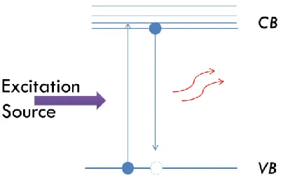
Figure 1: Photoluminescence due to absorption of light by an electron and subsequent
radiative relaxation during the transition between the conduction band (CB) and valance band
(VB). ... 4
Figure 2: Bulk-scale vs nano-scale showing energy level broadening due to QC effects ... 6
Figure 3: Electron-hole bound pair. This bound state can exist until such time as radiative or non-radiative relaxation occurs. ... 7
Figure 4: Photoluminescence as a result of mid-bandgap energy levels caused by defects in SiO2 film. ... 10
Figure 5: 1.7MV Tandetron Accelerator Schematic (Goncharova 2013)... 14
Figure 6:APL Spectroscopy Set-up ... 22
Figure 7: Time Resolved Photoluminescence Set-up ... 24
Figure 8: Zeeman Splitting in EPR showing energy level splitting ( with increasing magnetic field energy (B). ... 25
Figure 9: Stage 1 passivation intensity comparison. Double implant Sample 3 and 4 have lower intensity PL than the single implant Sample 1 indicating more quenching in these samples. ... 30
Figure 10: PL of Stage 1 samples, single and double implant with no hydrogen passivation. Highest intensity PL is from 90keV implant Sample 1 and lowest from the 1MeV + 90keV double implant Sample 4. The Y-axis represents the relative intensity of PL based on the most intense sample. ... 31
Figure 11: Simulated ion distribution for Sample 2 (right) and Sample 1 (left)... 31
vii
(right) with hydrogen passivation. 90keV single implant is compared to two double implant
samples. The Y-axis represents the relative intensity of PL based on the most intense sample
from each graph. ... 33
Figure 14: PL emission intensity and emission wavelength comparison between Stage 1 and
Stage 2 prepared samples with both single and double implants. The Y-axis represents the
relative intensity of PL based on the most intense sample, in this case 1.0 on the graph is
equal to the peak intensity of Sample 5. ... 34
Figure 15: TRPL radiative decay for double implant samples 1, 3 and 4 where is the
radiative lifetime modeled using a stretched exponential fit. ... 35
Figure 16: TRPL radiative decay for double implant samples 1, 3 and 4 modeled using a
triple exponential fit. ... 36
Figure 17: EPR signals from single and double as implanted unannealed samples. g-factors
Chapter 1
1
Silicon Quantum dots and Nanophotonics
Photonics is a popular area of research for applications in computing, information
processing and renewable energy technologies. The use of light for relaying information
with minimal losses over long distances has existed for thousands of years, a classic
example being the use of the Aldis Lamp as a reliable wireless communications device
for more than a century.
Although technology has come a long way in a relatively short period, we still use light
signals to relay information in fiber optic networks to interconnect electronic networks
around the world. One major challenge is miniaturization of photonic systems so that
light can be used not just in bulky interconnects between major networks but as an
integral part of device technologies we rely on and use on a daily basis. While fiber
optics is the backbone of the global information network, nanophotonics has the potential
to revolutionize our communications networks by taking the place of electronics in
interconnections and switches in data centers where systems run at very high capacities.
Far from electronics in every day devices becoming obsolete, developments in
nanophotonics for use in information bottlenecks can allow electronic communications to
realize their full potential. Excess heat in traditional electronics systems not only inhibits
performance but results in high energy consumption. Cooling is needed to maintain
optimal (or even minimal) performance. One only has to look at heat generated by the
microprocessor in a consumer laptop, which needs to be constantly cooled to prevent
system meltdown. It isn't an overstatement to say that possibly the most important part of
any computing system is cooling, without which the device would fail. Advancements in
nanophotonics and their application in everyday life could address many of these issues
leading to “greener”, more reliable and better performing information technologies and
renewable energy systems.
Si-QD and SiO2 luminescence is an area of much interest in nanophotonics.
subject of much research in the area of nanophotonics in the past two decades since the
discovery of PL from porous silicon in 1990 (Canham 1990). Many novel photonic and
optoelectronic devices such as solid state lighting (Humphreys 2008), optical chips
(Graydon 2007) and solar cell technologies (Liu 2010) have already been developed with
broad spectrum solid state lighting on consumer shelves already. Biological labeling
(Zhao 2010) and non-volatile memory devices (Cy 2007) are also possible applications
being investigated. In order for these devices to be developed for the market there is a
need for tunable light sources (Zhizhong 2009) manufactured using techniques
compatible with contemporary industrial methods. During the “Silicon Age” (Kittler
2006) many industrial processing techniques involving ion implantation into silicon have
been developed. Its use as a basis for new technologies such as some of those mentioned
above takes advantage of this fact. The synthesis of luminescent Si-QDs in SiO2 is
compatible with current industrial processes such as thin film growth via thermal
oxidation, ion implantation and crystal growth by rapid thermal annealing.
1.1
Photoluminescence
In this work we are investigating the mechanisms behind photoluminescence
(Dippo 2001) in Si-QD/SiO2 thin films. Si-QD photoluminescence (PL) and
electroluminescence (EL) (Pankove 1977) can be studied at room temperature which
makes the experimental process more convenient.
Semiconductor PL is the emission of a photon through radiative relaxation after the
absorption of light of high enough energy to cause interband electronic transitions. An
interband electronic transition is the promotion of an electron from the valence band to
the conduction band through the absorption of energy by the atoms in a material. Initially
the atoms in a photoluminescent material are not in an excited state, that is, there are an
equal number of holes in the valence band and electrons in the conduction band. In order
conduction band an electron must absorb a photon with energy corresponding, at a
minimum, to the bandgap energy of that material. The bandgap of a material is the energy
difference between the highest energy of the valence band and lowest energy of the
conduction band.
Conservation of energy implies that the frequency (v) of the incoming photon must
satisfy Eq.1 to impart enough energy for excitation.
(1)
where E is the energy of the incoming photon, h is the Planck constant, E1 is the highest
energy level of the valence band and E2 is the lowest energy level of the conduction band.
Once promoted to the conduction band an electron will spontaneously lose its excess
energy and relax back down to the valence band and at the same time emit a photon. The
relaxation process involves energy emitted as photons or energy dissipated as vibrations
in the surrounding material. The time scale of competing radiative and non-radiative
processes will influence their probability of occurrence and therefore the emission
efficiency of the material in question. If non radiative processes occur on a shorter time
scale than radiative processes then a material will emit little or no light. The frequency of
the emitted photon during de-excitation will correspond to the energy bandgap (Eg) of the
material.
1.1.1
Radiative Relaxation
Radiative relaxation occurs when an electron in a semiconductor material decays
or relaxes back down to the valence band from the conduction band with the emission of
a photon. The photon emitted will have a wavelength related to the energy difference
between the conduction band and the valence band of the material as mentioned in the
bandgap transitions the emitted light will be blue shifted and smaller bandgap transitions
will be red shifted.
1.1.2
Direct and Indirect Bandgap Semiconductors
In a direct bandgap semiconductor or an indirect bandgap material where the
transition rules are relaxed, electron decay from the conduction band to the valence band
can result in the emission of a photon.
Figure 1: Photoluminescence due to absorption of light by an electron and subsequent
radiative relaxation during the transition between the conduction band (CB) and valance
band (VB).
The emission photon will have a wavelength corresponding to the energy gap of the
material in question as is demonstrated in the operation of a Light Emitting Diode (LED).
The color of a LED is a result of photonic emission from semiconductor material
corresponding to the bandgap energy of that material. Silicon is an indirect bandgap
semiconductor meaning that exciton generation or the transition of an electron from the
valence band to the conduction band (excitation) is a two-step process. This is due to the
fact that the lowest energy level of the conduction band is not at the Brillouin zone center
so that it isn’t directly in line in with the highest energy level of the valence band. An
excitation to occur, so the absorption of both a photon and a phonon must occur at the
same time to ensure that energy and momentum are conserved and promotion of an
electron to the conduction band occurs (Streetman 1997). Under normal circumstances
this is very unlikely to occur in an indirect bandgap material given the offset band
structure. This effect is also apparent during relaxation of an electron from conduction
band to valence band of an indirect bandgap material where a phonon is needed. In an
indirect bandgap semiconductor such as silicon a phonon must add momentum to the
system at the same time as a photon is absorbed by an electron for transition of an
electron from the valence band to the conduction band. Relaxation or electron-hole
recombination is far less likely to be radiative resulting in emission of a photon.
Non-radiative recombination is dominant resulting in energy emitted as vibrations, dissipating
into the surrounding material without photoemission. In the case of Si-QD in SiO2 the
rules preventing radiative recombination are relaxed. This is due to electron confinement
playing a role in the recombination mechanism. An exciton exists as a coupling of an
electron in the conduction band and a “hole” in the valence band due to their Coulomb
attraction. This bound state results in the pair revolving around their center of mass
separated at a distance equal to that of the exciton Bohr radius. The Bohr radius is the
most probable distance between the hydrogen proton and electron given by the Eq. 2,
(2)
where is the permittivity of free space, is the reduced Planck’s constant, is the
electron rest mass and e is the elementary charge. The exciton Bohr radius is found by
applying the Bohr model to a free exciton as shown in Eq. 3,
(3)
where m0 is the mass of an electron, is the dielectric constant and is the
reduced mass of the exciton. Using this equation the exciton Bohr radius of silicon is
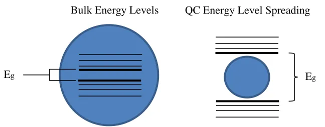
found to be 4.3nm in bulk crystalline silicon. In Si-QD with a radius approaching the
exciton Bohr radius, a widening of the energy bands occurs which is explained in Section
Figure 2: Bulk-scale vs nano-scale showing energy level broadening due to QC effects
This widening of energy bands increases the electron-hole separation, reducing the
probability of non-radiative recombination allowing for the main recombination route to
be radiative resulting in photo emission (Kovalev 1998). There exists an inverse
relationship between Si-QD diameter and photon emission energy, as diameter decreases,
energy of photons emitted increases as does their frequency. There is some evidence that
smaller radius quantum dots can transfer excitation to larger quantum dots in clusters
acting as donors with emission coming from the larger quantum dots (Jayatilleka 2011).
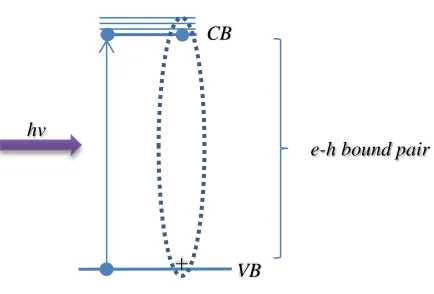
1.1.3
Excitons
Photon absorption followed by the promotion of an electron to an excited state
leaves a net positive charge in the valence band due to the lack of negative charge from
the electron. This net positive charge is referred to as a hole. Similarly the electron
carries a net negative charge to the conduction band. If the electron-hole binding energy
is greater than kBT where kB is the Boltzmann constant, then an exciton will form,
separated by and attracted due to the Coulomb force. The lifetime of the exciton
depends on whether its binding energy is strong enough to prevent it from coming into
contact with phonons. Fewer defects result in a longer lifetime. In semiconductors,
Bulk Energy Levels QC Energy Level Spreading
excitons exist as bound electron-hole pairs with separation distances of more than one
lattice constant.
Figure 3: Electron-hole bound pair. This bound state can exist until such time as
radiative or non-radiative relaxation occurs.
Since there is interaction between the electron and hole and they act as a bound
pair or exciton, they are not seen as separate but as one quasiparticle for the lifetime of
the exciton. Excitons occurring in semiconductors are known as Wannier excitons and
often result in radiative recombination. Wannier excitons can be considered as similar to
the hydrogen atom with one negative charge orbiting a positive charge. Adjusting the
model of the hydrogen atom with a Bohr radius of 0.05nm, the exciton Bohr radius in a
semiconductor can be calculated to be around 4.3nm. The weaker interaction as
compared to the Bohr model is due to the larger radius of the Wannier exciton. In the
hydrogen atom the electron is more tightly bound due to the larger relative mass of the
proton resulting in increased Coulomb force interaction and a smaller radius. Photon
emission due to the radiative recombination of Wannier excitons is a source of
luminescence in semiconductors and QC effects are seen when the size of a particle such
as Si-QD approaches the exciton Bohr radius.
VB hv
CB
+
1.2
Quantum Confinement
As mentioned in the previous section, the optical properties of nanostructures
differ from bulk materials due to spatial confinement of electrons and subsequent
broadening of energy levels within the particle. This spatial confinement results in
structures such as silicon quantum dots behaving like individual atoms with quantized
energy levels rather than a collection of atoms with degenerate energy levels. Bulk
material properties like degenerate energy levels give way to quantum properties such as
discontinuous energy bands and increased bandgap energy caused by the confinement of
electrons in up to three dimensions. Quantum Confinement (QC) effects are apparent as
the object dimension or quantum dot diameter in this case approaches ~5nm.
Photoluminescence typical of QC is usually in the red region of the visible spectrum (750
– 900nm) for Si-QD in SiO2 (Yu 1998).
1.3
SiO
2Defects
The presence of defects around Si-QD and in SiO2 films can have a significant
influence on the electronic and optical properties of Si-QDs. Defects studied here are
caused by the irradiation process. An intrinsic point defect may be classified as a
vacancy or a self-interstitial defect. A vacancy defect occurs when an atom is knocked
out of position, breaking bonds in the process. An interstitial defect occurs when
additional atoms (possibly knocked out of place by incoming Si ions) occupy interstitial
spaces in the SiO2. Either oxygen or silicon can be displaced during ion irradiation,
breaking Si-O bonds causing silicon and oxygen vacancies and silicon or oxygen excess
in different regions. During QD growth, defects occur at the interface between
Si-QDs and the surrounding SiO2. These defects are a byproduct of the crystallization
process resulting in dangling bonds with unpaired valence electrons which can quench
photoluminescence by acting as non-radiative recombination centers (Lee 2012). The
Si-QD/SiO2 interface. It is possible that the size and shape of the quantum dots is affected
by the number of vacancies present in the SiO2 before crystallization. During ion
implantation the implanted Si ions cause damage to the SiO2 film. This damage results in
vacancies where a Si or O atom has been knocked out of position and leaves a vacancy
behind which isn’t filled by another atom. During the annealing/crystallization step after
implantation these vacancies are filled by diffusing Si forming quantum dots.
1.3.1
Dangling Bonds
A dangling bond occurs in SiO2 when a silicon or oxygen atom is out of place and
unpaired electrons exist. These sites act to quench PL in unpassivated samples as
unpaired electrons trap holes and prevent radiative recombination of electron-hole pairs.
Dangling bonds are present at the Si/SiO2 interface and in areas where the SiO2 has been
damaged due to irradiation with silicon ions. Unpaired electrons are present at each
dangling bond site due to atomic vacancies. Hydrogen passivation can deactivate the
unpaired electrons to significantly reduce the number of dangling bonds present after
crystallization. Hydrogen atoms diffuse into the SiO2 film and terminate dangling bonds.
Determining the number of dangling bonds can indicate the scale of damage caused
during implantation which is thought to affect the formation of silicon quantum dots in
SiO2. Damage to the SiO2 host could free up excess silicon for the formation of Si-QDs
and at the same time control nucleation sites which may have an influence on the
Ostwald ripening process during Si-QD formation. Defect-mediated diffusion of silicon
atoms during the Si-QD growth process may also mean that the presence of defects in the
SiO2 can influence Si-QD growth and cluster formation (Mokry 2009). Damage can be
1.4
Defect luminescence in SiO
2SiO2 is transparent in the visible spectrum and has a large energy bandgap of
~9eV. Mid-bandgap energy levels result in luminescence due to electron transitions
between localized states and valence/conduction bands and vice versa.
Figure 4: Photoluminescence as a result of mid-bandgap energy levels caused by defects
in SiO2 film.
Interface states can act as electron and hole traps which quench actual Si-QD emission.
Defect PL in SiO2 emits higher energy/shorter wavelength light than Si-QDs with
emission in the blue/green region of the visible spectrum as opposed to Si-QD typical red
luminescence.
+
VB CB
hv PL
1.5
Thesis Overview
Due to many simultaneous processes during Si-QD photoluminescence in SiO2
extracting information from characterization techniques can be complex. The aim of this
work is to determine whether defects in the host material (SiO2) have an influence on the
growth and/or PL associated with Si-QDs in our samples. Defects and Si-QDs are
investigated using Electron Paramagnetic Resonance and PL spectroscopy in order to
determine how Si-QD growth and PL emission are affected by defects in SiO2. QC
effects of Si-QD or interface states on the surface of Si-QDs are also investigated. If
damage to the SiO2 film during implantation affects the growth of Si-QDs then it is
possible that Si-QD growth can be controlled by pre-implant damage induced in the SiO2.
If defect-related PL is present, it may have an influence on Si-QD PL. A number of
different preparation conditions are used to grow Si-QDs in SiO2. Results of
characterization techniques are assessed to form a more complete picture of processes
involved in the growth and properties of Si-QDs and the consequence of the abundance
of defects present in SiO2 due to ion irradiation. Defect-mediated diffusion of silicon
atoms and subsequently silicon nanoparticles during the Si-QD growth process could
have an influence on the distribution and size of Si-QDs in SiO2. If this is the case then
altering the structure of the SiO2 layer before implanting the Si-QD seed layer should
have an influence on the growth of Si-QDs in samples. Differences in Si-QD properties if
present should be noticeable by measuring the PL spectra and radiative lifetimes of
samples while varying preparation conditions. In this research Photoluminescence
spectra, Time Resolved Photoluminescence lifetime and Electron Paramagnetic
Resonance characteristics are compared using different pre-implant conditions and the
Chapter 2
2
Implantation and Growth
Silicon quantum dots are grown in an amorphous thermal oxide film of SiO2 in
this research. Silicon ions (Si+) are implanted into the oxide film at a predefined depth
and dose. Annealing promotes the growth of the silicon quantum dots and removes
damage to the oxide film which occurs during implantation. A further anneal step is
carried out in forming gas (5% H2: 95% N2). At 500oC hydrogen diffuses into the SiO2
film and terminates bonds which were broken during ion implantation. Broken bonds
with unpaired electrons act as luminescence quenching sites. Elimination of these
quenching sites results in increased luminescence intensity.
2.1
Thermal Oxide Film Growth
The thermal oxide SiO2 film used in this work is an amorphous thin film grown
using wet thermal oxidation of a crystalline silicon wafer to a depth of 280nm. This
material is used since it allows nucleation of Si-QD during annealing and a large
difference in band gap energy between SiO2 (insulator) and Si-QD can result in
photoluminescence with lower probability of quenching by SiO2 host material.
Thermal oxide films used in this research were not grown on site. The following
is a brief description of the thermal oxidation process. Wet thermal oxidation of silicon
wafer is achieved by exposing a silicon wafer to high temperatures in the presence of
pure steam. Crystalline silicon (c-Si) wafers are held vertically or horizontally in a tube
furnace during the process. Oxygen and hydrogen gasses are combined and heated to
high temperatures (>800oC) at which point they ignite. This reaction results in the
production of very high purity steam. The steam is then directed into the furnace
chamber with the c-Si wafer(s). Once the steam reaches the wafer surface an oxidation
SiO2. As the film thickness increases the oxidation process slows down. The slowdown
in this process is due to the fact that oxygen must diffuse through the oxide film to bond
with silicon atoms. Diffusion speed can be increased by increasing the processing
temperature but in order to ensure uniform and stoichiometric oxide growth the
temperature is kept constant, a 250nm film may take up to 24hrs to grow (Kang 2006).
2.2
Ion Implantation
Ion implantation is used in the Integrated Circuit (IC) manufacturing industry to
modify semiconductor materials. Using various elements the electronic properties of
semiconductors may be controlled and enhanced. For example, intrinsic semiconductors
(e.g. Si, Ge) have an equal number of electrons in their conduction band as holes in their
valance band at room temperature. Silicon has a relatively low bandgap (1.1eV) relative
to an insulator such as SiO2 (~9eV) but thermal energy at room temperature is
insufficient (kBT = 25meV@RT) for electrons to make it into conduction band so silicon
does not have sufficient charge carriers at room temperature to allow for significant
current flow. Using ion implantation intrinsic semiconductors can be altered to have an
excess of charge carriers, increasing concentration by up to several orders of magnitude
to allow vastly increased conduction. Implanted dopants can be n-type or p-type; acting
as electron donor or electron acceptor respectively within the silicon crystal lattice. For
example a dopant such as boron (p-type) is implanted beneath the surface of an intrinsic
semiconductor wafer such as silicon. Boron atoms act as electron acceptors in the
otherwise highly pure c-Si resulting in a p-type semiconductor with an excess of holes or
positive charges at room temperature. Si-QDs can be relatively easily grown using ion
implantation to implant silicon ions into SiO2 (Shimizu‐Iwayama 1994). In this work
silicon ions are implanted in a thin film of SiO2 to create an excess of silicon in the host
2.2.1
Implantation Process
The ion implanter consists of a number of sections including sputter source, low
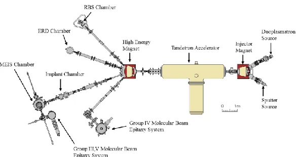
energy magnet, accelerator and implantation chamber. A schematic of the 1.7MV
Tandetron Accelerator at the University of Western Ontario (UWO) is shown in Figure 5
with the various stages labeled. At the ion source the ions necessary for implant are
extracted from the source surface. Ion sputtering is used to extract ions for use in
implantation in this research. A cesium source is ionized and Cs+ ions are accelerated
towards a cooled target consisting of the element to be implanted e.g. silicon. The idea
behind cooling the target is so that a thin layer of cesium coats the target surface, which
aids the sputtering process. The target surface is then sputtered due to bombardment with
Cs+ ions and negative target ions are ejected. The negative ions are injected into the main
accelerator chamber where a stripper gas strips electrons to form positive ions (e.g. Si+).
In the main accelerator chamber ions are accelerated to various energies from 50keV to
above 1MeV. Implant energies upwards of 1MeV using a medium energy medium
current implanter causes beam current drop off so that achieving an appropriate dose can
be prohibitively slow.
Figure 5: 1.7MVTandetron Accelerator Schematic (Goncharova 2013)
Only ions of the correct charge, mass and energy are wanted for implant so the beam
applying the correct magnitude of magnetic field the required ions are directed into the
final beam line toward the implant stage. Multiple exit lines are connected to this point
to allow for different ion trajectories to be selected. The beam line marked in red in
Figure 5 was used in this work. In order to implant more area without moving the sample
stage the beam passes through a raster scanner before reaching the sample surface. The
sample stage area is under vacuum during. This allows rapid pump down of the sample
chamber to reduce time spent loading and unloading the sample. Implantation is through
a circular aperture which is changed according to the desired implant area, up to 5cm2 is
possible. Charge build up at the sample stage can cause positive ions to be deflected
resulting in non-uniform implant therefore the sample is supplied with electrons to
neutralize charge. Implant Energy as well as ion mass determines the implant depth
profile. Increasing beam energy results in a deeper depth profile for a given ion species
but more massive ions result in a shallower depth profile for a given beam energy. For
example Si+ into SiO2 at 50keV implant energy will result in a peak concentration at
around 100nm below the SiO2 surface. 90keV beam energy will peak at around 120nm –
130nm depth. Dose depends on beam current during the implantation process. High
beam current means higher beam flux and a higher concentration of the implanted
element in the sample resulting in lower ion energy due to the larger number of ions to be
accelerated. Medium current/medium beam energy implant will result in a lower dose
with a deeper depth profile and high energy implanters use low dose for deep
implantation. Damage to the target material during ion implantation occurs due to
collisions between incoming ions and the target. Energy transfer from implanted
(incident) ions during impact causes subsequent collisions between nearby host
(secondary) atoms resulting in a damage cascade effect. For each single incident ion
multiple atoms in the host are displaced as each secondary ion transfers kinetic energy to
surrounding atoms. Collisions result in vacancy and interstitial defects in the sample.
Just as implanted ion concentration has a concentration profile with a peak at a certain
depth there is a similar vacancy profile with a peak concentration of vacancies/damage to
the target. These profiles can be estimated using Monte Carlo simulations run using
Stopping Range of Ions in Matter (SRIM) (Ziegler 2013) software in order to estimate
will sit nearer the surface than concentration profiles. Multiple energy implants can be
used to investigate the influence of damage in the SiO2 film on the growth of Si-QD.
First a high energy implant is performed which passes through the SiO2 film into the
silicon substrate to induce damage and afterwards a lower energy implant seeds the
Si-QD growth in the SiO2 film. Using this technique the damage can be controlled and
quantified to relate subsequent characteristics of Si-QD grown to different pre-implant
damage profiles.
2.3
Thermal Annealing
In IC manufacture Rapid Thermal Annealing (RTA) is used to activate dopants
(Kuhn 2010) and recrystallize areas of the silicon substrate which were damaged during
implantation. In this work thermal annealing is used to repair damaged SiO2 films and
enable growth of Si-QD. RTA is normally performed for only very short durations of
seconds at a time. Annealing here is done using a tube furnace and for this reason anneal
times are significantly longer and can be up to 2hrs since it is not a rapid thermal anneal
(Barbagiovanni 2011). In order to prevent further oxidation of the sample the initial
anneal step is performed in a nitrogen atmosphere at a temperature of 1100oC for 2hrs.
The second anneal stage is performed at 500oC and in a hydrogen/nitrogen atmosphere of
Forming Gas. At this temperature hydrogen diffuses into the SiO2 film and passivates
broken bonds (Dabrowski 2000).
2.3.1
Si-QD Growth
Nucleation of quantum dots occurs in the implanted region in the SiO2 film during
thermal annealing in the tube furnace at 1100oC. Although Si-O bonds occur
preferentially, the low diffusion rate of Si in SiO2 means that Si-Si bonds occur in the
dots occurs due to Ostwald Ripening as larger quantum dots grow at the expense of
smaller ones. Small quantum dots with a larger surface area to volume ratio are less
energetically stable than larger quantum dots. When the excess silicon is used up this
process will slow. As long as silicon is available to diffuse towards quantum dots the
average size will grow hence lower concentration implants result in smaller Si-QD
average size. It is possible that defect-mediated diffusion of Si atoms could have an
influence on the formation of silicon quantum dots in SiO2 with quantum dots forming in
areas where damage has occurred and broken bonds are present (Mokry 2009).
2.3.2
Hydrogen Passivation
Passivation of dangling bonds is achieved as the last stage in Si-QD synthesis
process. A dangling bond is an unsatisfied valence on an immobilized atom. Hydrogen
diffuses into the SiO2 and eliminates dangling bonds by taking the unpaired electron into
a bonding orbital. After the growth stage anneal in N2 for 2hrs at 1100oC the samples are
annealed at 500oC in forming gas (5% H2/N2) for 1hr. Forming gas is used in order to
eliminate the possibility of spontaneous combustion of hydrogen by mixing it with an
inert gas such as nitrogen. At 500oC hydrogen diffuses into SiO2 and bonds with any
available Si atom which has an unpaired electron by forming covalent bonds. A structure
which is created during the irradiation process and passivated by hydrogen during this
annealing is a silicon atom bonded to three oxygen atoms with an unpaired electron in a
sp3 orbital. This is present both in the SiO2 and at the Si-QD/SiO2 interface and has been
found to be an electron-hole trap site which quenches radiative emission. Fewer
unpaired electrons present increases the probability of radiative recombination by
eliminating mid-bandgap electron/hole traps where non radiative recombination can
occur. As shown in Table 2 in Chapter 4 samples were prepared with two stages of
annealing. Stage 1 is a sample set 1-5 with no hydrogen passivation and Stage 2 is a
sample set 1-5 with hydrogen passivation. These samples were prepared in order to
compare EPR spectra and PL spectra for both hydrogen passivated and non-passivated
Chapter 3
3
Experiment
Thermally grown oxide films of 280nm thickness were used as a host material for
Si-QD. These films were sourced from Silicon Sense Inc. The SiO2 films were
implanted at room temperature with Si+ ions at energies of 90keV, 400keV and 1MeV.
The projected peak implant depth of Si+ within the SiO2 film and c-Si substrate beneath
was estimated using SRIM simulation software to be 148nm, 654nm and 1.38µm
respectively. Only the 90keV implant range is within the 280nm SiO2 film. Prior to
implantation the silicon wafers were cut using a diamond tip scribe into ~5cm2 pieces for
mounting onto the implant chamber stage. A 5cm2 implant area was used for the 400keV
and 1MeV samples and a 3cm2 implant area was used for the 90keV sample with lower
dose. Different implant areas were used due to the implant dose chosen, a higher implant
dose requires more implant time therefore the smaller implant area was used for the
90keV sample with lower dose. Ion dose for the 90keV implant was
with used for both the 400keV and 1MeV implants. All implants
carried out are listed in Table 1. Each energy/dose was implanted onto an individual
wafer so that reference samples could be kept. After implantation, samples were cut into
1cm2 sections in order to allow for different preparation stages to be compared. Si-QD
growth was carried out in a quartz tube furnace at 1100oC for duration of 2hrs in a high
purity nitrogen atmosphere. The tube furnace was pumped down to ~50mTorr with a
roughing pump and nitrogen gas was allowed to flow through according to the
procedures supplied. The furnace heater was programmed according to the operation
manual supplied, allowing 50min for ramp up to 1100oC, 2hrs at the required temperature
and approximately 3hrs for cool down. During ramp up and cool down periods the
samples were placed inside the quartz tube but outside the heated area in order to ensure
that the anneal time was 2hrs and no longer. During the temperature ramp up it is
important to monitor gas flow as it fluctuates as the temperature increases, usually two
adjustments are necessary to ensure that gas flow remains constant during ramp up. A
passivation anneal was carried out to reduce the effects of non-radiative electron-hole
recombination. Each sample was annealed in forming gas (5%H2:N2) at 500oC for 1hr.
Between the growth stage anneal and the hydrogen passivation step, samples were left
inside the furnace and the same procedure for preparing the furnace atmosphere was
followed, this time with forming gas. The same temperature ramp up procedure was
followed, this time maximum anneal temperature was set to 500oC.
PL spectroscopy sample size was 1cm2. These measurements were performed at
McMaster University, Hamilton. The excitation source is a 2mW continuous power
325nm HeCd laser with 1mm beam diameter and intensity of ~64mW/cm2. The beam is
passed through a ½” aperture onto the sample without focusing. The PL emission is
collected by an achromatic objective lens and focused into a fiber optic patch by an
achromatic lens. The optical fiber is Ocean Optics model QP600-2-VIS-NIR. The
spectrometer is an Ocean Optics model ADC1000 and is connected to a PC. Ocean
Optics software is used to collect and process the data. Origin Pro 8 software was used to
correct and smooth the data afterwards. No special sample preparation was undertaken
for these measurements and they were carried out at room temperature.
TRPL spectroscopy was performed at room temperature using a pulsed 405nm
laser diode as the excitation source. The laser driver is a 405nm laser diode driver with
potentiometer and Transistor-Transistor Logic (TTL) switching purchased from O-Like
lasers (www.o-like.com). The TRPL set up is housed in a light sealed box,
measurements were taken with lab lights on and off and no difference was observed. The
experimental set up was identical to that shown in Figure 7 with a 450nm high-pass
Thorlabs filter placed in front of the PMT in order to filter out reflected UV light from
the sample. The laser was focused onto the sample using a focusing lens to create a beam
diameter of ~1mm at which point the most intense PL was observed in the each sample.
The waveform generator was set to a pulse frequency of 500Hz with 200µs pulse width.
Although higher frequency pulsing would allow a larger sample rate, 500Hz was selected
in order to extend laser diode life. PL emission was collected using a Hamanatsu
R7400U-20 Photomultiplier Tube (PMT) set to -800V and output measured with a
the oscilloscope from the waveform generator using a T-connection. Each sample was
irradiated for 2min before the decay trace was saved. Exponential averaging with 20
frame sample storage was used with 14bit sampling.
Samples selected for ESR measurements were removed after the growth anneal
step and before the passivation step. All PL spectroscopy was performed before ESR
measurements were taken since ESR requires a smaller sample size therefore further
cutting of the samples. ESR spectroscopy measurements were performed with a Jeol
JES-FA200 system at room temperature on unpassivated samples. Sample preparation
for ESR spectroscopy involved further sectioning of samples into 4mm x 7mm pieces due
to the sample size needed to fit into the quartz tube for ESR measurements. After cutting
the samples were sonicated in a sonic bath for 15min in order to remove any
contamination. Each sample was placed in the ESR system under vacuum. ESR
measurements were then collected with the sample exposed to a DC magnetic field
varying between 328mT and 340mT which causes the splitting of singly-occupied
electron energy levels into sublevels corresponding to parallel and antiparallel electron
spin orientations and an AC field at a frequency of 9.5GHz which induces optical
transitions between these sub-levels. The resultant spectra were collected and graphed
using Origin Pro 8 graphing software. No further modeling has been done on these
spectra as of yet.
4
Characterization Techniques
Photoluminescence Spectroscopy and Time-Resolved Photoluminescence
Spectroscopy (TRPL) are non-destructive characterization techniques used here to probe
electronic states in Si-QD/SiO2 films. Both Si-QD and defects in SiO2 show
photoluminescence (PL). For the most part they emit light in different spectral regions
and so are distinguishable with PL Spectroscopy although some Si-QD/SiO2 interface
states exhibit PL at a similar wavelength (red) to Si-QDs (Pacchioni 2000). TRPL is a
more specific tool bringing with it more complex data. Interpreting radiative decay
in order to extract information regarding mechanisms. Si-QD/SiO2 films contain defects,
oxide interfaces and quantum dot clusters each possibly contributing to the PL radiated.
Electron Paramagnetic Resonance (EPR) is a technique used here to investigate the
electron spin of atoms in Si-QD/SiO2 films. Paramagnetic defects contain unpaired
electrons which can be detected using EPR. Depending on the strength and shape of the
EPR signal collected, different the types of dangling bonds can be identified as each
unpaired electron is affected by its local environment i.e. the surrounding atomic species.
4.1
Photoluminescence Spectra
Photoluminescence spectroscopy involves irradiation of a sample with light in
order to cause interband electronic transitions. Light emitted by the sample is then
collected and displayed as a spectrum using a spectrometer. It is a non-destructive
method for investigating the electronic structure of materials by irradiation with
UV-Vis-IR radiation. PL spectroscopy is a relevant experimental method in this research as it can
be used to identify defects in oxides and to characterize semiconductor nanostructures.
Photoemission from these materials can provide information about concentrations of
defects and size distribution of nanostructures under various preparation conditions. Due
to QC effects, nanostructures like Si-QDs can emit energy in the form of photons which
gives information about their properties and the surrounding host material. PL
spectroscopy is a common tool for investigating Si-QD and silicon nanoclusters and
studies have been carried out on luminescence of nitride passivated silicon nanoclusters
(Wilson 2011), non-radiative recombination centers in silicon in silicon nitride
(Gritsenko 1999) and rare earth metals (Kudo 1997) to name but a few. PL spectroscopy
normally is performed at room temperature. Alternatively if sample cooling is necessary
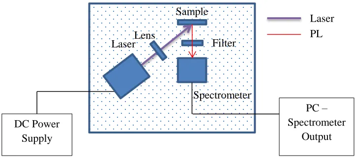
Figure 6: APL Spectroscopy Set-up
A typical PL Spectroscopy set up includes an excitation source such as a laser. The
excitation laser wavelength is sample dependent in that the photon energy must be higher
than the bandgap energy of the material under investigation. A mirror is used to direct
the laser beam onto the sample so that the beam spot can be easily adjusted without
disturbing the laser housing. A lens or lenses are necessary to focus the emitted light
from the sample into a spectrometer for light collection. Fixed or variable wavelength
lasers are used to excite electrons in the sample material from the valence band into the
conduction band and the intensity of emitted light is recorded as a function of
wavelength. Photoemission due to interband electronic recombination is the source of
light collected at the spectrometer. Direct bandgap semiconductors exhibit
photoluminescence upon the absorption of a photon. As mentioned in Section 1,
photoluminescence is not a usual characteristic of indirect bandgap semiconductors such
as bulk crystalline silicon, but nanostructures such as Si-QDs in SiO2 do exhibit strong
PL at room temperature when excited with UV light (Mokry 2009). PL spectra due to
defects and oxide interface states at the Si-QD/SiO2 interface are dominated by low
intensity emission wavelengths in the visible spectrum but blue shifted (500nm – 600nm)
in comparison to PL due to QC effects (700nm – 900nm) in Si-QD structures. Radiative
recombination of electron-hole pairs in due to defects has a shorter emission wavelength
since the energy bandgap is larger resulting in higher energy emission. Defect related PL
can indicate the concentration of defects in a sample due to damage during ion
irradiation. While defect PL is eliminated by annealing and hydrogen passivation it is
thought that knowledge of the concentration of defects in a sample prior to the Si-QD
growth stage can help to understand more about the growth mechanisms of Si-QDs in
SiO2. PL spectra and Time Resolved PL are the two main experimental techniques used
here to characterize Si-QDs in SiO2.
4.2
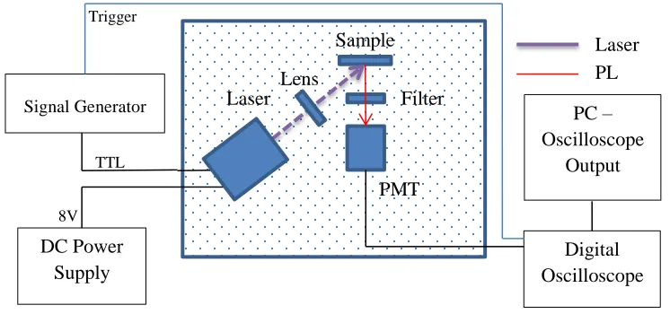
Time-Resolved Photoluminescence
Time-resolved Photoluminescence (TRPL) spectroscopy is based on the same
physical principles as PL spectroscopy in that excitation of the sample with light causes
interband electronic transitions resulting in photon emission due to electron-hole
recombination. Time-resolved PL spectroscopy is used extensively to identify QC effects
or to distinguish QC based emission from defect related PL in SiO2 (M.Dovrat 2004)
(Dohnalova 2009). In PL spectroscopy a continuous wave (CW) laser is used as an
excitation source and the wavelength of photons emitted is recorded. In TRPL
spectroscopy measured here the radiative lifetime of emission is observed using a pulsed
laser source, PMT and digital oscilloscope. Radiative recombination lifetimes of Si-QDs
in SiO2 are an area attracting attention in the last decade although debate as to exactly
what mechanisms are involved and how the resultant data should be interpreted is
ongoing. As an experimental technique this method can provide information on Si-QD
properties as a function of growth conditions. The radiative lifetime (τ) varies depending
on Si-QD size. QC lifetimes have been found to have a size dependent range between – (Garcia 2003) but whether this is due only to QC or includes interface and
defect related PL is debatable. High resolution measurements necessitate shorter pulse
widths on the order of nanoseconds for excitation in order to record equally short decay
lifetimes but longer lifetimes from upwards can be observed with a longer pulse
Figure 7: Time Resolved Photoluminescence Set-up
QC related PL emission from Si-QD is a quasi-direct process due to the fact that there is
a high probability of radiative recombination. It is described here in terms of direct gap
transitions. The radiative lifetime (τ) of observed decays vary depending on contributing
structures, interface states, vacancy defects or QC from Si-QDs. During laser excitation
an electron absorbs energy from an incident photon supplied by the excitation source, and
is promoted from the ground state at the valence band (VB) to an excited state above the
conduction band (CB). Due to the promotion of the electron a hole is created at the VB
energy level. The electron goes through a number of rapid ( ) relaxation processes.
Excess (>Eg) energy dissipates to the lattice and the electron relaxes to the edge of the
bandgap corresponding to this lowest energy level in the CB. During the radiative
recombination process the electron decays back to the ground state (VB) and in doing so
emits energy in the form of a photon with energy corresponding to Eg. TRPL measures
the length of time over which radiative processes like this occur. Relaxation times above
the conduction band where energy is lost as heat are fast enough to be negligible; the
most important information is contained in the length of time emission occurs after the
excitation source is turned off.
4.3
Electron Paramagnetic Resonance
Electron Paramagnetic Resonance (EPR) is used to study paramagnetic centers
indicative of unpaired electrons in ions and molecules. Its principles are similar to those
of Nuclear Magnetic Resonance (NMR). While the NMR spectrum is a result of nuclear
spin, as the name suggests the, EPR spectrum is the result of the electron spin magnetic
moment. NMR has a wide variety of uses especially in the medical. Any element with
nuclear spin can be investigated using NMR whereas in the case of EPR not all materials
will have unpaired electrons. In materials that do contain paramagnetic centers such as
unpaired electrons in dangling bonds, EPR is a powerful tool since it can probe highly
specific regions such as nanostructures. Paramagnetic defects are significant in that they
are caused by paramagetism due to unpaired electrons.
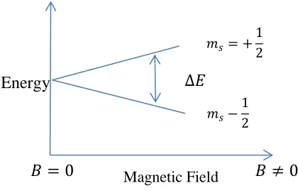
Figure 8: Zeeman Splitting in EPR showing energy level splitting ( with increasing
magnetic field energy (B).
Electron spin magnetic moment is highly dependent on its surroundings and
interactions with other species in a given sample so the resultant EPR spectrum is
sensitive to sample preparation and external interference which can cause noise in the
signal. Observable features which are of interest in this study include interfacial oxide
states (Si-QD/SiO2) and defects containing dangling bonds with unpaired electrons where
atoms (Si or O) have been displaced due to ion irradiation. An electron has a spin
magnetic moment ( ) due to spin about its axis represented by depending on
orientation. Electrons in full or bonding orbitals are paired, one spin up and one spin Energy
Magnetic Field
𝑚𝑠 +
𝐸
𝑚𝑠
down, according to the Pauli Exclusion Principle. This paired configuration is
diamagnetic, meaning one electron is in the state and the other electron is in the
+ state. An unpaired electron will be paramagnetic meaning that a single
unpaired electron will be either in the state or in the + state with no
opposite spin electron present. Unpaired electrons can be detected using EPR
spectroscopy. In the presence of a magnetic field previously degenerate energy levels
split due to the Zeeman Effect. Electron transitions can now be induced from lower to
higher energy levels through the absorption of energy. Usually the magnetic field is
varied in the presence of a fixed microwave frequency in the region of 9GHz. As the
magnetic field increases, the difference in the energy levels widen, and when the
difference ( between the two levels equals the energy supplied by the microwave
signal ( , absorption occurs. Usually the first derivative of the resultant absorption
spectrum is displayed. Without the presence of the microwave signal the unpaired
electrons are distributed almost equally between and + according to
the Maxwell-Boltzmann law. When the resonance condition is met, unpaired
electrons transition from the lower energy level to a higher energy level and in the
process must change spin from the state to the + state. The EPR
spectrum resonance condition will depend mainly on spin-orbit coupling. An unpaired
electron is promoted to + and relaxes back to in a short period of time
so that electrons in state, and electrons in the + state do not equalize.
Spin-lattice relaxation occurs when energy is lost to the lattice. This is a slower process
and is usually negligible. The splitting of energy levels due to the Zeeman effect is
directly proportional to the magnetic field strength as shown in Equation 2.
(4)
where is the difference between energy levels due to Zeeman Splitting. is the
proportionality constant between the observed electron magnetic moment and the
involves the influence of surrounding nuclei on unpaired electron spin. This can give
insight into the local environment of the electron i.e. what species it is associated with.
PL intensity has been found to be strongly linked to the density of unpaired electrons in
SiO2 (Hiller 2010). A difference between the existence of interface unpaired electrons
Chapter 4
5
Results and Discussion
Si-QD samples were prepared using ion beam implantation to seed Si+ ions in a
thermally grown SiO2 oxide film on silicon substrate. Samples were implanted with three
implantation energies and two concentrations of Si+ ions. Table 1 shows the sample set
indicating which samples received double implants and the energy and dose used.
Sample 1 was implanted with a single dose of Si+ and implant energy
of 90keV. Sample 3 was initially implanted with a dose of , implant
energy of 400keV and subsequently implanted with a single dose of Si+
at an energy of 90keV. Similarly Sample 4 was initially implanted with a dose of
at an energy of 1MeV and subsequently implanted with a single dose of Si+
at an energy of 90keV. Samples 2 and 5 were implanted with a dose
of at energies of 400keV and 1MeV respectively. The intention of an
initial high energy implant is to induce defects in the 280nm thick SiO2 film. 400keV and
1MeV implant energies into the silicon substrate cause vacancies and broken bonds in the
SiO2 which could mediate Si-QD growth and influence PL characteristics. PL
spectroscopy measurements were performed at McMaster University, Hamilton, Ontario
using a 325nm HeCd laser excitation source. TRPL measurements were taken using a
405nm laser diode excitation source at UWO. As illustrated in Figure 6 this set up uses a
405nm air cooled laser diode as excitation source and a Hamamatsu R7400U-20 PMT for
light collection. A 450nm high pass filter was placed between the sample and the PMT
in order to filter out reflected source light which would oversaturate the PMT and obscure
any PL from the sample. The PMT was connected to a Cleverscope CS320A digital
oscilloscope which displays two channels A and B. Channel A is the PMT signal and the
Channel B signal is taken from the function generator which switches the laser on and off
at 200Hz with a variable pulse width. During the initial setting up of the system a 1Ω
resistor was added to the laser driver circuit in series and the voltage drop across it was
monitored and displayed on Channel B in order to measure the current through the laser
monitor the TTL pulse signal to the laser. This triggering source is more stable than the
previous set up as the voltage drop taken across the resistor was causing interfering with
the PMT output signal resulting in deterioration of the signal and excessive noise at
on/off points. Extensive measurements were taken to establish the minimum pulse width
possible and the overall resolution of the system. Combining the function generator and
the TTL-activated laser diode driver, the excitation pulse width could be reduced to as
low as 50ns and a clear signal was still detected by the PMT. Increased pulse frequencies
serve to speed up data collection but decrease the life of the laser diode. Pulse frequency
was not increased beyond 1 kHz for this reason. Sample saturation was found to occur at
pulse widths between 120µs and 200µs. Increasing pulse widths from 50ns up to sample
saturation were used to test whether pulse width had any influence on the radiative
lifetimes. Attempts were made to establish if pulse width and power variations had
similar effects. A trim pot was introduced into the circuit to allow for variable laser
power measurements to be taken. The resistor was varied between 0 Ω and 100 Ω in
order to observe if there was any variation in radiative lifetime from samples.
5.1
Silicon Quantum dot Photoluminescence
Photoluminescence emission spectra were collected from unpassivated and
passivated samples. Stage 1 samples were implanted and annealed but no hydrogen
passivation was carried out. At Stage 2 Si-QD are present in the SiO2 film. Absorption
spectra have not yet been calculated for these samples.
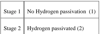
Stage 1 No Hydrogen passivation (1)
Stage 2 Hydrogen passivated (2)
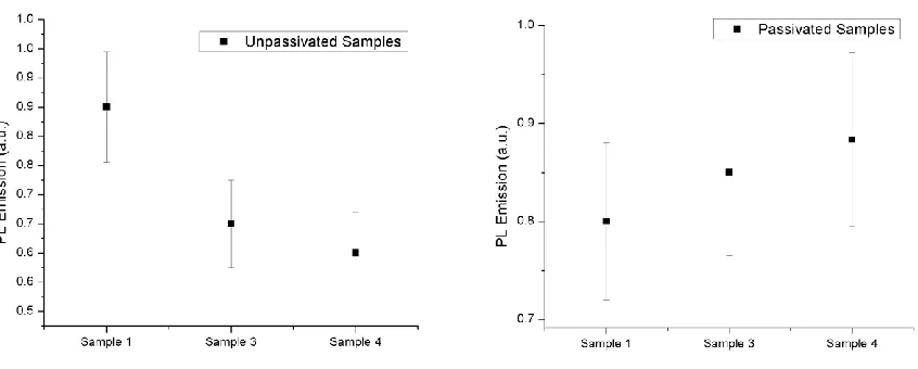
Table 1:Passivation Stage 1 and 2.
Figure 9 shows the PL intensity trend between unpassivated and also passivated samples
while the passivated samples seem to show a trend towards higher intensity PL with
increasing implant energy although the errors associated suggest the need for a larger
sample set.
Figure 9: Stage 1 passivation intensity comparison. Double implant Sample 3 and 4
have lower intensity PL than the single implant Sample 1 indicating more quenching in
these samples.
Figure 10 shows a comparison of single and double implant samples. Here PL is
more intense from the unpassivated single implant 90keV sample when compared to
double implant unpassivated samples. Reduced PL in unpassivated double implant
Figure 10: PL of Stage 1 samples, single and double implant with no hydrogen
passivation. Highest intensity PL is from 90keV implant Sample 1 and lowest from the
1MeV + 90keV double implant Sample 4. The Y-axis represents the relative intensity of
PL based on the most intense sample.
SRIM simulation software was used to simulate the implantation profiles for all implants
in order to estimate implant depth profiles and vacancy profiles.
Figure 11: Simulated ion distribution for Sample 2 (right) and Sample 1 (left)
As seen in Figure 11 the peak ion concentration for (90keV) Sample 1 is calculated at
the higher energy at 551.8nm (5518 Å). Importantly for this experiment the
concentration of Si+ in the SiO2 layer in Sample 2 is low enough to be negligible as is
also the case with Sample 4 and 5 implants at energy of 1MeV. Further experimental
work needs to be carried out in order to confirm these simulated ion ranges and vacancy
plots.
Figure 12: Vacancy profile for Sample 2 (left) and Sample 5 (right)
SRIM vacancy profiles in the SiO2 film are shown in Figure 12 and are
progressively deeper with increasing implant energy. The vacancy profile within the
SiO2 layer is higher, roughly doubled for the 400keV pre-implanted sample when
compared to the 1MeV pre-implanted sample due to the deeper damage profile of the
1MeV implant. The ionization profile is larger in the SiO2 film for the 1MeV pre implant
than the 400keV implant. It is possible that the difference in PL intensity between
samples is partly due to the ionization profile influence on Si-QD growth. At low energy
ion implantation (<100keV) nuclear stopping dominates where target damage is caused
by the incoming ions colliding with the nuclei of the substrate material. However for the
same ion at higher implant energies electronic stopping dominates where ionization
causes heating in the substrate material. This heating is due to ionization of the substrate
atoms through collisions with incoming ions. Double implant samples in this work have
electronic stopping profiles which are significantly larger in the 1MeV and 400keV
unpassivated the single implant 90keV sample shows more intense PL when compared to
the double implant samples in Figure 10 indicating more efficient emission from the
single implant sample due to less quenching. PL collected from hydrogen passivated
samples in Figure 13 and 14 shows the most intense PL in the 1MeV double implant
sample followed by 400keV double implant and 90keV single implant respectively.
These results show a reversal in intensity order from Stage 1 between the 1MeV and the
single implant 90keV sample indicating an improvement in PL efficiency in the sample
with a double implant.
Figure 13: PL of Stage 1 samples (left) with no hydrogen passivation and Stage 2
samples (right) with hydrogen passivation. 90keV single implant is compared to two
double implant samples. The Y-axis represents the relative intensity of PL based on the
most intense sample from each graph.
Given how close these intensity peaks are to one another and taking into account a 5%
standard deviation associated with the raw data more samples need to be tested but the
trend does indicate increasing intensity for Si-QD samples grown in SiO2 in which
damage was induced by a high energy initial implant of ions into the silicon substrate
Figure 14: PLemissionintensity and emission wavelength comparison between Stage 1
and Stage 2 prepared samples with both single and double implants. The Y-axis
represents the relative intensity of PL based on the most intense sample, in this case 1.0
on the graph is equal to the peak intensity of Sample 5.
The sample represented by the blue line (circle markers) in Figure 14 underwent double
implantation of 1MeV and then 90keV Si+ at doses of and
respectively gains most from the hydrogen passivation meaning that some gain in
PL intensity is possible due to excess defects already present or induced in the SiO2 film
prior to implantation of excess Si+ for growth of Si-QD
5.2
Time Resolved Photoluminescence: Decay Lifetimes
TRPL results conducted on Stage 2 samples indicate a slight difference in
radiative lifetimes in Samples 3 and 4 but a longer radiative lifetime for Sample 1 when
fitted using a stretched exponential fitting model. Pulse duration is 200µs for all TRPL
Si-QD diameters for double implant Sample 3 and 4. The decay data obtained from
experiments using the TRPL set up shown in Figure 15 and 16 are fitted stretched
exponential and triple exponential models. Both fitting methods result in a good fit with
adjusted r2 factors of close to 1. The stretched exponential fitting model shown in
Equation 3 is used for comparison between samples.
(5)
where is the average relaxation lifetime of the sample and is the stretching factor
limited between 1 and 0. This function assumes an infinite number of decay mechanisms
and the resultant average lifetime is used here to compare samples.
Figure 15: TRPL radiative decay for double implant samples 1, 3 and 4 where is the
Triple exponential fitting is also used and results show a similar trend towards
shorter radiative lifetimes with higher energy double implanted samples for the longest
radiative lifetime. Plots are shown in Figure 16 and lifetime data in Table 3.
Figure 16: TRPL radiative decay for double implant samples 1, 3 and 4 modeled using a
Radiative Lifetimes
Sample 4 (1MeV + 90keV)
(+ ⁄
Sample 1 (90keV)
(+ ⁄
Sample 3 (400keV + 90keV)
(+ ⁄
τ1 220 212 205
τ2 63.6 56.1 56.1
τ3 9.15 7.99 8.17
Table 2: PL radiative lifetime (
τ
1) results using triple exponential fitAs seen from the PL Spectroscopy results there is a peak emission wavelength
shift between samples 1 and 4 possibly demonstrating different average Si-QD size with
larger Si-QD demonstrating longer radiative lifetime emission (Garcia 2003). It is
understood that with decreasing Si-QD size comes a blue shift which is evident in these
data. Without TEM images as yet it is not possible to definitively say if in fact the
average Si-QD size differs between samples but results from PL spectra do show changes
in PL emission intensity and a wavelength shift.
5.3
Electron Paramagnetic Resonance: Paramagnetism
and Dangling Bonds
Results from EPR are preliminary and given the complexity of the sample and the
qualitative nature of the measurements more data and analysis is necessary to develop a
clearer picture of paramagnetism as a result of dangling bonds in these samples. What
can be seen from the data collected is that when compared to the manganese reference
signal the EPR signal from each unannealed sample differs in a way which is to be
expected judging by the implant conditions. This information is useful in that it tells us
that although a large portion of each sample is made up of the silicon substrate, EPR may
still be able to shed some light on the as implanted structure of the samples in the 280nm