Power Electronics Technology for Power
Quality Improvement
M. Deben Singh
1, L. Khumanleima Chanu
2Assistant Professor, Department of Electrical Engineering, NERIST, Nirjuli, Arunachal Pradesh, India 1
PG Student, Department of Electrical Engineering, NIT, Agartala, Tripura, India2
ABSTRACT: The technological progress in the field of power electronics in the recent years has been achieved due to the advancement in power semi conductor devices which in turn have directly affected the power electronics converter technology and its application. Power electronics technology has affected every aspect of electrical power system networks including HVDC transmission system apart from AC transmission, distribution, utilization and also at generation level (e.g. static AVR). In this paper, an attempt has been made to study the performance of a power electronics based Custom power controller, DVR for use in the distribution network so as to enhance power quality and supply to the end consumers using MATLAB/ SIMULINK. Results of the simulation runs are also presented with various settings of parameter used in the model so as to support the validity of the role of DVR in improving the quality of power supply at distribution side.
KEY WORDS: DVR (dynamic voltage restorer), AVR (automatic voltage regulator), FACTS (flexible alternating current transmission system), HVDC (high voltage direct current transmission), VSC (voltage source converter), STATCOM (static synchronous compensator), UPFC (Unified Power Flow Controller), VSI (voltage source inverter).
I. INTRODUCTION
The application of power electronics controllers in the power distribution system to supply good quality electrical power to the consumers have become a major emphasis for the power supply providers in the deregulated power system environment. The quality of electrical power which is supplied to the customers can be judged in terms of constant voltage magnitude i.e., no voltage sags or swell, constant frequency, constant power factor, balanced phases, sinusoidal waveform i.e. no harmonic constant, lack of interruptions and capability to withstand faults and to recover quickly. The main components of an electrical power system are generators, transformers, transmission lines, loads, protection and control equipments. These components are interconnected so as to enable the generation of electricity in the most suitable locations and insufficient quantity to satisfy the customer‟s demand, to transmit it to the load centre and to deliver good quality electric energy at competitive prices.
Power electronic controllers are being developed to help generators operate reliably in the new market place. The voltage source converter (VSC) is the basic building block of the new generation of power electronics controllers emerging from FACTS and custom power research. In HV transmission, the most promising equipments include the STATCOM, UPFC and the HVDC light. At the low voltage distribution level, the VSC provides the basis for the distribution STATCOM (D-STATCOM), DVR and active filters. The last decade has seen a marked increase in loads that are sensitive to poor quality power supply. Some large industrial customers are critically dependent on uninterrupted electrical power supply and suffer large financial losses as a result of even minor losses in the quality of power supply. These factors coupled with the ongoing deregulation and open access electricity markets, where large consumers may shop around for competitively priced, high quality electricity have propelled the distribution industry into unprecedented change [1].
technology. Although FACTS and custom power initiations share the same technological base; they have different technical and economic objectives as:
FACTS systems controllers are aimed at the transmission level whereas custom power controllers are aimed
at the distribution level particularly at the point of connection of the electricity distribution on company with clients with sensitive loads and independent generators.
Custom power focuses primarily on the reliability and quality of power flows. However, voltage regulation,
voltage balancing and harmonic cancellation may also benefit from this technology.
The D-STATCOM and DVR are the two best known Custom Power Controllers/ equipments. The D-STATCOM and
the DVR both use VSCs but the D-STATCOM is a shunt connected device which may include the functions of voltage
control, active filtering and reactive power control. The DVR is a series connected device which precisely compensates for wave form distortion and disturbances in the neighborhoods of one or more sensitive loads. The D-STATCOM used in custom power applications uses PWM switching control as opposed to the fundamental frequency switching strategies which is preferably used in FACTS applications. PWM switching is practically used in custom power applications as it is at relatively low power level [1, 3, 9, 10]. In this paper, theoretical studies on the various aspects of power electronics and DVR have been carried out and an attempt has been made by studying a typical DVR model using MATLAB/SIMULINK. The simulation run results under different settings of the parameters used in the model have been presented so as to support its suitability for use in the electrical power distribution system.
1.1 POWER SWITCHING DEVICES: The various power switching devices may be classified into three categories with respect to the manner in which they can be controlled:
a) Uncontrolled switch: The diode belongs to this category. Its on or off state is controlled by the power circuit.
b) Semi-controlled switch: The thyristor or silicon controlled rectifier (SCR) is controlled by a gate signal to
turn-on. However, once it is on, the controllability of the device is lost and the power circuit controls when the device will turn-off.
c) Fully–controlled switch: Over the last twenty years a number of fully controlled power semiconductors have
been developed. This category includes the main kind of transistors such as the bipolar junction transistor (BJT) and the metal oxide semiconductor field effect transistor (MOSFET). New hybrid devices such as the insulated gate bipolar transistor (IGBT), the gate turn-off thyristor (GTO).
1.2 THYRISTOR: The SCR, simply referred to as thyristor is a semi-controlled four layer power semiconductor with three electrodes, namely, the anode (A), the cathode (K) and the gate (G). Since it is a four-layer device, it possesses three junctions. A two-transistor based analog can be used to explain the operating characteristics of the device. An
ideal thyristor exhibits infinite resistance to positive anode current unless a positive current pulse IG is supplied through
the gate. Then, the thyristor enters its on state and its resistance becomes zero. It remains at this state till the anode
current becomes zero. If the gate pulse IG is then zero, the thyristor resumes its initial state and its initial state of having
infinite resistance from the anode to the cathode to positive anode current. However, it should be noted that the anode
current does not become zero even when the gate pulse current IG becomes zero when the thyristor is on. This is the
most significant difference between the thyristor and the other fully controlled semiconductors [1,2].
1.4 INSULATED-GATE BIPOLAR TRANSISTOR (IGBT): The IGBT is a three-terminal power semiconductor device, noted for high efficiency and fast switching. This type of switch is used in many modern appliances viz. electric cars, variable speed motor drives, refrigerators, air-conditioners, and even stereo systems with switching amplifiers. Since it is designed to rapidly turn on and off, amplifiers that use it often synthesize complex waveforms with pulse width modulation and low-pass filters. The IGBT combines the simple gate-drive characteristics of the MOSFETs with the high-current and low–saturation-voltage capability of bipolar transistors by combining an isolated gate FET for the control input, and a bipolar power transistor as a switch, in a single device. The IGBT is used in medium- to high-power applications such as switched-mode high-power supply, traction motor control and induction heating. Large IGBT modules typically consist of many devices in parallel and can have very high current handling capabilities in the order of hundreds of amps with blocking voltages of 6,000 V [1, 2].
1.5 GATE TURN-OFF THYRISTOR (GTO): A gate turn-off thyristor (GTO) is a special type of thyristor, a high-power semiconductor device. GTOs, as opposed to normal thyristors, are fully controllable switches which can be turned on and off by their third terminal known as the gate. The ordinary thyristor (e.g. SCR) is not a fully controllable switch as a fully controllable switch can be turned on and off at will. The GTO can be turned-on by a gate signal, and can also be turned-off by a gate signal of negative polarity. Turn on is accomplished by a "positive current" pulse between the gate and cathode terminals. As the gate-cathode behaves like PN junction, there will be some relatively small voltage between the terminals. The turn on phenomenon in GTO is however, not as reliable as an SCR (thyristor) and small positive gate current must be maintained even after turn on to improve reliability. Turn off is accomplished by a "negative voltage" pulse between the gate and cathode terminals. Some of the forward current (about one-third to one-fifth) is "stolen" and used to induce a cathode-gate voltage which in turn induces the forward current to fall and the GTO will switch off (transitioning to the 'blocking' state.)GTO thyristors suffer from long switch off times, whereby after the forward current falls, there is a long tail time where residual current continues to flow until all remaining charge from the device is taken away. This restricts the maximum switching frequency to approx 1 kHz. It may however be noted that the turn off time of a comparable SCR is ten times that of a GTO. Thus switching frequency of GTO is much better than SCR [1, 2].
II. ADVANCEMENT IN POWER SWITCHING DEVICES
The performance of the semiconductors can be achieved by replacing silicon with Silicon carbide (SiC), Semiconducting diamond, Gallium Arsenide etc. The first group of devices is the most promising technology. These new power semiconductor materials offer a number of interesting characteristics such as large band gap, high carrier mobility, high electrical and thermal conductivity etc. Because of having these characteristics, these new class of power switching devices offer a number of positive attributes viz. high power handling capability, operation at high frequency ranges, relatively low voltage drop when conducting and operation at high junction temperatures. Such devices will be able to operate at temperatures up to approximately 600°C. It is anticipated that this technology will probably offer semiconductors with characteristics closer to the desired ones discussed in the previous section. Another important development is associated with the matrix converter (direct AC-AC conversion without a DC-link stage). For this converter bidirectional self commutated devices are needed to build the converter. At the moment research efforts show some promising results. However, a commercial product is probably not going to be available before the next decade or so [1]. Progress in semiconductor devices achieved over the last twenty years and anticipated developments and improvements promise an exciting new era in power electronic systems. Snubber less operation of fully controlled semiconductors at high values of current and voltage and their rates of change will be realizable in the near future. New emerging applications of these semiconductors in areas such as Power Transmission and Distribution and High Voltage Industrial Motor Drives will be possible. The thyristor will remain the only component for certain applications, due to its unmatched characteristics. However, expected improvements of the GTO and IGBT technology and emerging new devices may replace it sooner than later [1].
III. POWER ELECTRONIC CONVERTER
(i) Voltage source converter (VSC) or voltage-source inverter (VSI): In this type of converter, the DC bus input is a voltage source (typically a capacitor) and its current through can be either positive or negative. This allows power flow between the DC and AC sides to be bidirectional through the reversal of the direction of the current.
(ii) Current source converter (CSC) or current-source inverters (CSI):In this type, the DC bus input is a current
source (typically an inductor in series with a voltage source) and its voltage across can be either positive or negative. This also allows the power flow between the DC and AC sides to be bidirectional through the reversal of the polarity of the voltage.
The conventional phase-controlled thyristor based converters can only be current source systems. The modern converters based on fully controlled semiconductors can be of either type. In most reactive power compensation applications, when fully controlled power semi conductors are used, the converters used are of voltage-source based. However, the conventional thyristor-controlled converters are still used in high power applications and conventional HVDC systems [1, 2, 9].
3.1 APPLICATIONS OF VOLTAGE SOURCE CONVERTER: A voltage-source converter is a power electronic
device, which can generate a sinusoidal voltage with any required magnitude, frequency and phase angle. Voltage source converters are widely used in adjustable-speed drives, but can also be used to mitigate voltage dips. The VSC is used to either completely replace the voltage or to inject the „missing voltage‟. The „missing voltage‟ is the difference between the nominal voltage and the actual. The converter is normally based on some kind of energy storage, which will supply the converter with a DC voltage. The solid-state electronics in the converter is then switched to get the desired output voltage. Normally the VSC is not only used for voltage dip mitigation, but also for other power quality issues, e.g. flicker and harmonics.
3.2 VSC IN SERIES VOLTAGE CONTROLLER (DVR): The series voltage controller is connected in series with the protected load. Generally, the connection is made via a coupling transformer, but configurations with direct connection via power electronics system also exist. The resulting voltage at the load bus bar equals the sum of the grid voltage and the injected voltage from the DVR. The converter generates the reactive power needed while the active power is taken from the energy storage. The energy storage system can be different depending on the needs of compensation. The DVR often has limitations on the depth and duration of the voltage dip that it can compensate [5, 9].
3.3 VSC IN SHUNT VOLTAGE CONTROLLER (D-STATCOM): A D-STATCOM consists of a two-level VSC, a dc energy storage device and a coupling transformer connected in shunt to the distribution network. The VSC converts the dc voltage across the storage device into a set of three-phase ac output voltages. These voltages are in phase and coupled with the ac system through the reactance of the coupling transformer. Suitable adjustment of the phase and magnitude of the D-STATCOM output voltages allows effective control of active and reactive power exchanges between the D-STATCOM and the ac system. Such configuration allows the device to absorb or generate controllable active and reactive power [5].
IV. INTRODUCTION TO DYNAMIC VOLTAGE RESTORER SYSTEM
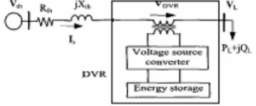
The DVR system is a type of Custom Power controller which is designed to have excellent dynamic performance capable of protecting critical and/or sensitive load against short duration voltage dips and swells. The DVR consists of energy storage unit, VSC and injection transformer as shown in figure 1.
The DVR is connected in the utility primary distribution feeder. This controller is suitable for solving a variety of power quality and reliability problems such as voltage sags and swells, voltage unbalances, harmonics, power factor correction, outages etc. The DVR injects a set of three phase ac voltages in series and synchronised with the distribution feeder voltages of the ac system. The amplitude and phase angle of the injected voltages are variable thereby allowing control of the active and reactive power exchanges between the DVR and the ac system within predetermined positive (power supply), and negative (power absorption) limits [1,5, 9.10].
4.1 MAIN COMPONENTS OF DVR: The main components of DVR are energy storage system, voltage source
converter circuit, filter unit and series injection transformer. These are discussed below:
(a). ENERGY STORAGE SYSTEM: The energy needed for the DVR can be extracted from an auxiliary supply
(topologies with energy storage) or grid itself (topologies with no energy storage) for compensation of load voltage during sag. The auxiliary supply method is applied to increase the performance when the grid of DVR is weak. In this type, variable DC link voltage or constant DC link voltage topologies are applied. In second topology, the remaining voltage on supply side or load side is used to supply necessary power to the system if the DVR is connected to the strong grid. In load side connected topology, the DC link voltage is almost constant because it is always fed from corrected constant load voltage [7]. The load side connected converter topology is selected for this study.
(b). VSC CIRCUIT: The voltage source converter circuit caters variable output voltages required for the DVR system. Solid-state semiconductor devices with turn off capability are used in inverter circuits. The VSC is energized by a stiff DC voltage supply of low impedance at the input. The output voltage is independent of load current. In VSCs, the values of output voltage variations are relatively low due to capacitor. It is difficult to limit current because of the capacitor. The three phase pulse width modulation (PWM) based VSC is the most popular and common inverter type and it is being used in this study. The voltage control is achieved by modulating the output voltage waveform within the inverter [7, 9].
(c) FILTER SYSTEM: As the output voltage of VSC generally contains harmonics, filter system is used to solve such problem. The inverter side and line side filtering are basic types of filtering scheme. The inverter side filter is closer to the harmonic source and low voltage side thus it prevents the harmonic currents to penetrate into the series injection transformers. This can cause voltage drop and phase shift in the fundamental component of the inverter output. The line side is closer to high voltage side so higher rating on transformer is needed. The filter voltage drop and phase shift problem don‟t disturb this system. In both filtering schemes, filter capacitor will cause increased inverter ratings. The increased filter capacitor provides better harmonic attenuation but the rating of the inverter is related with the capacitor value. The inverter side filtering method is being used in this study [1, 7, 9].
(D) SERIES INJECTION TRANSFORMERS: The three single-phase injection transformers are used to inject
missing voltage to the system. The electrical parameters of series injection transformer should be selected correctly to ensure the maximum reliability and effectiveness. To integrate the injection transformer correctly into the DVR, the MVA rating, the primary winding voltage and current ratings, the turn-ratio and the short-circuit impedance values of transformers are required [1, 7, 9,10].
4.2 OPERATING MODES OF DVR: The DVR can operate in three modes viz.: protection mode, standby mode
(during steady state) and injection mode (during sag).
(i). PROTECTION MODE: The DVR is protected from the over current in the load side due to short circuit on the
load or large inrush currents. The bypass switches remove the DVR from system by supplying another path for current. (ii). STANDBY MODE: In standby mode (normal steady state conditions), the DVR may either go into short circuit operation or inject small voltage to compensate the voltage drop on transformer reactance or losses. Short circuit operation of DVR is generally preferred solution in steady state because the small voltage drops do not disturb the load requirements if the distribution circuit is not weak.
V. SIMULATION RESULTS AND DISCUSSIONS
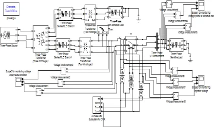
A Matlab/simulink model of the DVR as shown in figure 2 has been developed for study under various parameter settings. The energy storage system has been realized by connecting a dc voltage source and the 3-phase VSI along with its necessary control circuits have been incorporated in VSI subsystem of the model. The various voltage waveforms under different conditions are monitored by three Scopes viz. Scope1, 2 and 3. The Scope1 is meant for monitoring the voltage profile at the sensitive load, Scope2 for monitoring voltage waveforms under fault conditions and Scope3 has been connected for observing the voltage injection waveforms at the secondary sides of the series injection transformers. The model has been simulated using IGBT and GTO switches in the VSI used in the DVR system.
Figure 2: Simulink model of the DVR
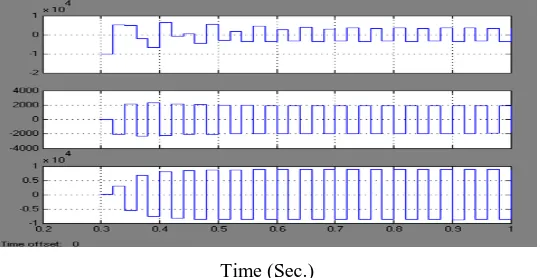
(i) RESULTS OF SIMULATION RUNS WITH IGBT SWITCHES: Figure 3 (a) shows the output voltage
waveforms under line to ground fault condition.
Time (Sec.)
Figure 3: (a) Fault voltage waveforms
V
ol
tag
e (
V
o
lt
In figure 3 (b), it shows that the DVR system injects the necessary 3-phase voltages in order to compensate the voltage
sag occurring across the load,
Time (Sec.)
Figure 3: (b) Injected voltage waveforms
Figure 3 (c) shows the compensated output voltage waveforms across the load after injecting voltage by the DVR system.
Time (Sec.)
Figure 3: (c) Compensated output voltage waveforms
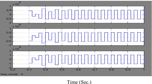
(ii) RESULTS OF SIMULATION RUNS WITH GTO SWITCHES: The model when simulated under single line to ground fault condition using GTO switches in the VSC circuit produced the same sag / fault voltage waveforms asdepicted in figure 3 (a). The injected voltage waveforms from the DVR are shown in figure 4(b).
Time (Sec.)
Figure 4: (a) Injected voltage waveforms
V
ol
tag
e (
V
o
lt
s
)
V
ol
tag
e (
V
o
lt
s)
V
ol
tag
e (
V
o
lt
The compensated output voltage waveforms for all the 3 phases are depicted in figure 5 (b).
Time (Sec.)
Figure 4: (b) Compensated output voltage waveforms
VI. CONCLUSION
In this paper, the role of power electronics based controllers used in the power system operation with special emphasis on Custom power controller by taking up a DVR model as example has been discussed. From the simulation results of the DVR model studied, it is observed that the shapes of output waveforms remain almost same when IGBT and GTO switching devices are used in the VSI circuit. It is also learnt that the voltage sag occurring at the distribution level under fault conditions is highly undesirable for the power consumers with their sensitive loads and this problem can be mitigated by introducing a well designed DVR system.
REFERENCES
[1] E Acha, V G Agelidis, O Anaya-Lara and T J E Miller, “A text book on Power Electronic Control in Electrical Systems”, ELSEVIER Publication, First Printed in India, 2006.
[2] Muhammad H. Rashid, “A text book on Power Electronics: Circuits, Devices, and Applications”, Pearson Education Publication, Fourth Indian Reprint, 2005.
[3] Hingorani, N.G., “Introducing Custom Power”, IEEE Spectrum, Vol.32, No. 6,pp. 41-48, June 1995.
[4] Hingorani, N.G., “Flexible AC Transmission Systems”, IEEE Spectrum, Vol. 30, No. 4, pp. 41-48, April 1993.
[5] S.V Ravi Kumarand S. Siva Nagaraju, “Simulation of D-Statcom and DVR in Power Systems”, APRN Journal of Engineering and Applied Sciences, Vol. 2, No. 3, pp. 7-13, June 2007.
[6] Hingorani, N.G.,” Power Electronics in Electric Utilities: Role of Power Electronics in Future Power Systems”, Proceedings of the IEEE, Vol. 76, No. 4, pp. 481-482, April 1998.
[7] Mehme Tümay, Ahmet Teke, K. Çağatay Bayındır and M. Uğraş Cuma, “Simulation and Modeling of a Dynamic Voltage Restorer”, Eleco‟s 4th International Conference on Electrical and Electronics Engineering, Vol.4, pp. 1-5, Turkey, 2005.
[8] Hingorani, N.G., “High Voltage DC transmission: A Power Electronics Workhorse”, IEEE Spectrum, Vol. 33, No.4, pp.63-72, April 1996.
[9] Arindam Ghosh and Gerard Ledwich, “A text book on Power Quality Enhancement using Custom Power Devices”, Springer International Edition, 2009.