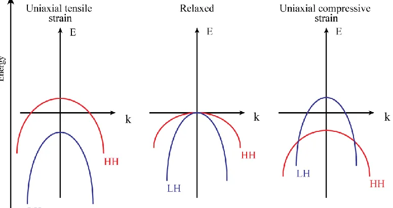
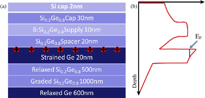
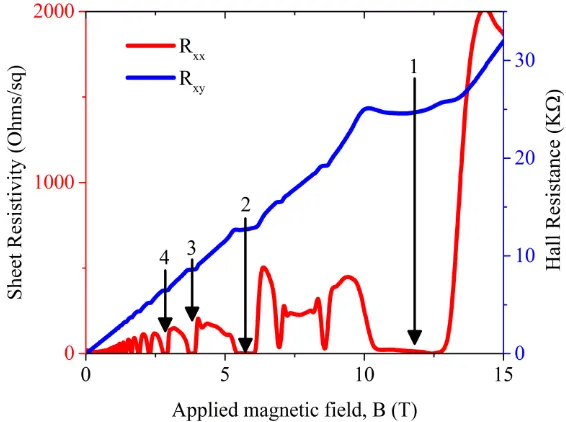
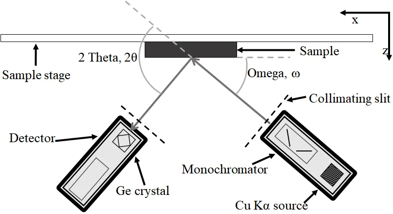
Fractional quantum phenomena of 2DHGs within strained germanium quantum well heterostructures
Full text
Figure
Outline
Related documents
Dabral V, Kapoor S andDhawan S, spline finite element method to get numerical solutions of one dimensional heat Equation.. Kannan, 2012) is one of the relatively new
Three formulations of tooth paste were prepared by vary- ing the concentrations (%) of ingredients viz, guava leaf powder, Acacia arabica gum powder, sea salt, stevia herb
Figure S2 a Compatibility of S and FeO content of Mercury’s mantle with pressure of metal/silicate equilibration for various core S contents (1, 2, 5 and 7 wt%), using Chabot
Relative to consumers who fit into their expected size, those who encountered larger sizes were less likely to purchase additional sized items (i.e., clothing), and more likely
conventional KOSs the modelling of relations falls short, while natural language is used for defining intra-term relations which allow for the creation of complex concepts.. But
Information about open graduate positions and early career entry programmes can be found on our career website at www.airbus.com/work.. Most roles can be accessed by clicking
Investing in emerging markets, impose the need to know the world’s two main accounting systems: Generally Accepted Accounting Principles (GAAP) and International
Emphasis will be on the evolution of accounting as an academic subject inside the institution of higher education from Transylvania, the Academy of High Commercial and
