UNIX™
MICROSYSTEM
WE®
32100
MICROPROCESSOR
INFORMATION MANUAL
MAXI COMPUTING
IN
MICROSPACE
UNIX™
MICROSYSTEM
WE® 32100
MICROPROCESSOR
INFORMATION MANUAL
ACKNOWLEDGEMENTS
Prepared and published by
Document Development Organization - Microelectronics Projects Group AT&T Technologies, Inc., Morristown
for the
Microsystem Product Management AT&T Technologies, Inc.
and the
4516 Microsystems Laboratory AT&T Bell Laboratories, Holmdel
A
WORD ABOUT TRADEMARKS
The following trademarks are mentioned in this manual:
W£® 32100 Microprocessor
W£® 32101 Memory Management Unit
W£® 32102 Clock
W£® 321AP Microprocessor Analysis Pod
W£® 321DS Microprocessor Development System
W£® 321EB Microprocessor Evaluation Board
W£® 321SD Development Software Programs
W£® 321SE Software Evaluation Program
W£® 321SG Software Generation Programs
are registered trademarks of AT&T Technologies, Inc.
AT&T 3B20S Computers is a trademark of AT&T.
UNIX™ Operating System is a trademark of AT&T Bell Laboratories.
PDp™ 11170 Computer and V AXTM 111780 Computer are trademarks of Digital Equipment Corporation.
IBM® 370 Computer is a registered trademark of the IBM Corporation.
_ ATSaT
WE®
32H)0 Microprocessor
KmformatioHll MamliaR
FOREWORD
This manual contains information on the WE 32100 Microprocessor that is essential to computer designers, software architects, and system design engineers. The support software and development tools available simplify system integration for this complex 32-bit microprocessor. This issue contains a description of the version SVR2.0 of the
WE 321SG Software Generation Programs.
Additional information is available in the form of data sheets, application notes, and on-line documentation from the UNIX Operating System.
For additional information contact your Sales Account Representative or call: o Commercial sales: 1-800-372-2447
o AT&T and Associated Company sales: (215) 770-3204 or (CORNET) 8+624-3204. To obtain additional copies of this manual, Select Code 451-000, call:
WE 32100 MICROPROCESSOR INFORMATION MANUAL
CONTENTS
CHAPTER 1. INTRODUCTION
1. Introduction ... 1-1 1.1 Overview ... 1-1 1.2 Architecture ... 1-2 1.3 Instruction Set... 1-4 1.4 Operating System Support... 1-4 1.5 Software Generation Programs... 1-5
CHAPTER 2. ARCHITECTURE AND BUS OPERATION
2.7.1 Faults... 2-30 Fault With SRDy... 2-32 Fault After DTACK... 2-33 2.7.2 Retry ... 2-34 2.7.3 Relinquish and Retry ... 2-34 2.8 BLOCKFETCH SPECIAL CASES .. .,... 2-37 2.8.1 Fault on First Word of Blockfetch With Status Code Other Than Prefetch ... 2-37 2.8.2 Fault on First Word of Blockfetch With Status of Prefetch ... 2-37 2.8.3 Retry on First Word of Blockfetch ... 2-37 2.8.4 Retry on Second Word of Blockfetch... 2-37 2.8.5 Relinquish and Retry of Blockfetch ... 2-42 2.9 INTERRUPTS ... 2-42 2.9.1 Interrupt Acknowledge ... 2-42 2.9.2 Auto-vector Interrupt... 2-45 2.9.3 Nonmaskable Interrupt... 2-45 2.9.4 Quick Interrupt ... 2-48 2.10 BUS ARBITRATION ... 2-48 2.10.1 Bus Request During a Bus Transaction ... 2-48 2.10.2 DMA Operation ... 2-51 2.11 RESET ... 2-52 2.11.1 System Reset ... 2-52 2.11.2 Internal Reset ... 2-52 2.11.3 Reset Sequence... 2-54 2.12 ABORTED MEMORY ACCESSES ... 2-54 2.12.1 Aborted Access on PC Discontinuity With Instruction Cache Hit... 2-55 2.12.2 Alignment Fault Bus Activity... 2-56 2.13 SINGLE-STEP OPERATION ... 2-57 2.14 COPROCESSOR OPERATIONS ... 2-58 2.14.1 Coprocessor Broadcast ... 2-58 2.14.2 Coprocessor Operand Fetch... 2-63-2.14.3 Coprocessor Status Fetch... 2-64 2.14.4 Coprocessor Data Write... 2-65 2.15 EXCEPTIONAL CONDITIONS ... 2-66 2.16 TRACE MECHANISM ... 2-69 2.17 PIN ASSIGNMENTS ... 2-70 2.18 MICROPROCESSOR OPERATING REQUIREMENTS ... 2-83 2.18.1 Electrical Requirements ... 2-84 2.18.2 Clocking Requirements ... 2-85 2.18.3 Thermal Requirements ... 2-85 2.19 SUPPLEMENTARY PROTOCOL DIAGRAMS ... 2-87
CHAPTER 3. INSTRUCTION SET AND ADDRESSING MODES
Return from Procedure (RET) ... 3-98 Return on Greater Than or Equal (Signed) (RGEQ) ... 3-99 Return on Greater Than or Equal (Unsigned) (RGEQU) ... 3-100 Return on Greater Than (Signed) (RGTR). ... 3-101 Return on Greater Than (Unsigned) (RGTRU) ... 3-102 Return on Less Than or Equal (Signed) (RLEQ) ... 3-103 Return on Less Than or Equal (Unsigned) (RLEQU) ... 3-104 Return on Less Than (Signed) (RLSS) ... 3-105 Return on Less Than (Unsigned) (RLSSU) ... 3-106 Return on Not Equal (RNEQ, RENQV» ... 3-107 Rotate (ROTW) ... 3-108 Return from Subroutine (RSB) ... 3-109 Return on Overflow Clear (RVC) ... 3-110 Return on Overflow Set (R VS) ... ... 3-111 Save Registers (SAVE) ... 3-112 Coprocessor Operation (no operands) (SPOP) ... 3-113 Coprocessor Operation Read (SPOPRS, SPOPRD, SPOPRT) ... 3-114 Coprocessor Operation, 2-Address (SPOPS2, SPOPD2, SPOPT2) ... 3-115 Coprocessor Operation Write (SPOPWS, SPOPWD, SPOPWT) ... 3-116 String Copy (STRCPY) ... 3-117 String End (STREND) ... 3-119 Subtract (SUBB2, SUBH2, SUBW2) ... 3-120 Subtract, 3 Address (SUBB3, SUBH3, SUBW3) ... 3-121 Swap (Interlocked) (SWAPBI, SWAPHI, SWAPWI) ... 3-122 Test (TSTB, TSTH, TSTW) ... 3-123 Exclusive Or (XORB2, XORH2, XORW2) ... 3-124 Exclusive Or, 3 Address (XORB3, XORH3, XORW3) ... 3-125 3.7.3 Instruction Set Summary by Function ... 3-126 3.7.4 Instruction Set Summary by Mnemonic ... 3-132 3.7.5 Instruction Set Summary by Opcode ... 3-136
CHAPTER 4. OPERATING SYSTEM CONSIDERATIONS
CHAPTER 5. SOFTW ARE GENERATION PROGRAMS
5. INTRODUCTION TO THE SOFTWARE GENERATION
GLOSSARY AND ACRONYMS
INDEX
LIST OF FIGURES
Figure 1-1. The WE 32100 Microprocessor ... 1-1 Figure 1-2. WE 321AP Microprocessor Analysis Pod ... 1-3 Figure 1-3. WE 321EB Microprocessor Evaluation Board ... 1-3
Figure 2-1. Figure 2-2. Figure 2-3. Figure 2-4. Figure 2-5. Figure 2-6. Figure 2-7. Figure 2-8. Figure 2-9. Figure 2-10. Figure 2-11. Figure 2-12. Figure 2-13. Figure 2-14. Figure 2-15. Figure 2-16. Figure 2-17. Figure 2-18. Figure 2-19. Figure 2-20. Figure 2 -21. Figure 2-22. Figure 2-23. Figure 2-24. Figure 2-25.
Figure 2-26.
Figure 2-27. Figure 2-28. Figure 2-29. Figure 2-30. Figure 2-31. Figure 2-32. Figure 2-33. Figure 2-34. Figure 2-35.
WE 32100 Microprocessor Block Diagram ... . Programmer's Model for User Registers ... . Processor Status Word ... . Bit Order of Data ... . Bit Field Data Type ... . Signal Sampling Points ... . Read Transaction (Using SRDY) ... .
Read Transaction (Using DT ACK) ... .
Read Transaction with One Wait Cycle (Using SRDY) ... ..
Read Transaction With Two Wait Cycles (Using DTACK) ... ..
Write Transaction (Using SRDY) ... .
Write Transaction (Using DTACK) ... .
Write Transaction With Two Wait Cycles (Using SRDY) ... .
Write Transaction With One Wait Cycle (Using DTACK) ... .
Read Interlocked Transaction (Using DTACK).. ... ..
Blockfetch Transaction (Using SRDY) ... ..
Blockfetch Transaction (Using DT ACK) ... .
Blockfetch Transaction (Using DTACK) ... .
Blockfetch Transaction (Using SRDY) ... .
Asynchronous Fault Without DTACK and SRDY (Read Transaction) .. . Fault with Synchronous Ready (SRDY); i.e., Synchronous Fault ... . Fault After Assertion of DTACK (Write Transaction is Shown) ... . Retry of Transaction (Read Transaction is Shown) ... . Relinquish and Retry ... . Fault on First Word of Blockfetch Transaction
With Access Status Code (Not Instruction Prefetch) ... . Fault on First Word of Blockfetch Transaction
With Access Status Code of Prefetch ... . Retry on First Word of Blockfetch Transaction ... . Retry on Second Word of Blockfetch ... . Interrupt Acknowledge ... . Auto-Vector Interrupt Acknowledge ... . Nonmaskable Interrupt Acknowledge ... . Bus Request During a Transaction ... . Reset Sequence ... . Aborted Access on I-Cache Hit with PC Discontinuity ... . Alignment Fault Bus Activity (Write Transaction is Shown) ... .
Figure 2-38. Coprocessor Command and ID Transfer... 2-59 Figure 2-39. Coprocessor Command and ID Transfer
(No Coprocessor Present) ... 2-62" Figure 2-40. Coprocessor Operand Fetch ... 2-63 Figure 2-41. Coprocessor Status Fetch (Using SRDY) ... 2-64 Figure 2-42. Coprocessor Data Write... 2-65 Figure 2-43. WE 32100 Microprocessor Pin Configuration... 2-71 Figure 2-44. Read Transaction Followed by a Read Transaction ... 2-88 Figure 2-45. Read Transaction Followed by a Write Transaction
(Using DTACK) ... 2-89 Figure 2-46. Write Transaction Followed by a Write Transaction ... 2-90 Figure 2-47. Write Transaction Followed by a Read Transaction ... 2-91 Figure 2-48. Double-Word Program Fetch Without Blockfetch
Transaction (using DTACK) ... 2-92 Figure 2-49. Bus Arbitration During Relinquish and Retry ... 2-93
Figure 3-1. Bit Order of Data... 3-2 Figure 3-2. Bit Order in a Bit Field ... 3-2 Figure 3-3. Extending Data to 32 Bits ... 3-5 Figure 3-4. Register as a Source Operand ... 3-5 Figure 3-5. General Instruction Format ... 3-7 Figure 3-6. Data Embedded in an Operand ... 3-7 Figure 3-7. Expanded-Operand Type Descriptor ... 3-21 Figure 3-8. Condition Flags ... 3-22 Figure 3-9. Stack After CALL-SAVE Sequence... 3-31
Figure 4-1. A Typical Process Control Biock ... "... 4-8 Figure 4-2. Tables for the Gate Mechanism ... 4-15 Figure 4-3. A PCB on an Initial Process Switch to a Process ... 4-19 Figure 4-4. A PCB on a Process Switch During Execution of a Process ... 4-20 Figure 4-5. An Interrupt Stack... 4-26 Figure 4-6. Interrupt Vector Tables ... 4-27 Figure 4-7. Exception-Vector Table ... 4-31 Figure 4-8. Virtual Address Fields for a Contiguous Segment ... 4-37 Figure 4-9. Virtual Address Fields for a Paged Segment... 4-37 Figure 4-10. Virtual to Physical Translation for Contiguous Segments ... 4-38 Figure 4-11. Virtual to Physical Translation for Paged Segments ... 4-39
LIST OF TABLES
Table 2-1. Processor Status Word Fields ... 2-5 Table 2-2. Memory Write Summary ... 2-10 Table 2-3. Simultaneously Asserted Exception Conditions ... : ... 2-30 Table 2-4. Interrupt Level Code Assignments ... 2-44 Table 2-5. Interrupt Acknowledge Summary ... 2-50 Table 2-6. Output Signal States after DMA Request is Acknowledged ... 2-51 Table 2-7. Output States on Reset ... 2-53 Table 2-8. Exception Conditions... 2-66 Table 2-9. Truth Table for Trace Trap ... 2-69 Table 2-10. WE 32100 Microprocessor Pin Descriptions ... 2-72 Table 2-11. Address and Data Signals ... 2-75 Table 2-12. Interface and Control Signals ... 2-76 Table 2-13. Access Status Signals ... 2-77 Table 2-14. Interrupt Signals ... 2-79 Table 2-15. Arbitration Signals ... 2-80 Table 2-16. Bus Exception Signals ... 2-81 Table 2-17. Development System Support Signals ... 2-83 Table 2-18. Clock Signals ... 2-83 Table 2-19. Operating Requirements ... 2-85 Table 2-20. Output Electrical Specifications ... 2-86 Table 2-21. Input Electrical Specifications ... 2-86
Table 3-1. Register Set ... ... ... 3-4 Table 3-2. Addressing Modes ... 3-9 Table 3-3. Options for type in Expanded-Operand Mode ... 3-21 Table 3-4. Data Transfer Instruction Group... 3-24 Table 3-5. Arithmetic Instruction Group ... 3-25 Table 3-6. Logical Group... 3-27 Table 3-7. Program Control Instructions... 3-29 Table 3-8. Coprocessor Instructions... 3-33 Table 3-9. Stack and Miscellaneous Instructions... 3-33 Table 3-10. Condition Flag Code Assignments ... 3-34 Table 3-11. Assembly Language Operators and Symbols ... 3-36 Table 3-12. Data Transfer Instruction Group ... 3-126 Table 3-13. Arithmetic Instruction Group ... 3-126 Table 3-14. Logical Group... 3-128 Table 3-15. Program Control Instructions ... 3-129 Table 3-16. Coprocessor Instructions... 3-131 Table 3-17. Stack and Miscellaneous Instructions... 3-131 Table 3-18. Instruction Set Summary by Mnemonic ... 3-132 Table 3-19. Instruction Set Summary by Opcode ... 3-136
Table 4-4. Severity Levels for Exceptions ... 4-30 Table 4-5. Normal Exceptions (ET=3) ... 4-33 Table 4-6. Stack Exceptions (ET=2) ... 4-34 Table 4-7. Process Exceptions (ET=I) ... 4-35 Table 4-8. Reset Exceptions (ET=O) ... 4-36
Chapter 1
CHAPTER 1. INTRODUCTION
CONTENTS
INTRODUCTION
Overview
I. INTRODUCfION
This chapter introduces the WE 32100 Microprocessor and summarizes the support products available for it. The chapters describing the WE 32100 Microprocessor
architecture, instructiun set, operating system considerations, and software generation programs are also introduced.
1.1
Overview
The WE 32100 Microprocessor is a high-performance, single-chip, 32-bit central processing
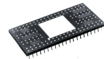
unit designed for efficient operation in a high-level language environment. The WE 32100 Microprocessor represents a state-of-the-art concept in microprocessor architecture, providing one of the most powerful and extensive instruction sets available with any microprocessor. The WE 32100 Microprocessor, packaged in.a I 32-pin ceramic pin array, is shown on Figure I-I.
Figure 1-1. The WE 32100 Microprocessor
The system memory space is addressed over a full 32-bit address bus using either physical
or virtual addresses. The 32-bit address bus produces a vast memory space of more than
four billion bytes which increases the flexibility of memory organization and provides ample space for the storage of software and data. Data can be read or written over the
separate 32-bit data bus in byte (S-bit), halfword (16-bit), or word (32-bit) lengths. The WE 32100 Microprocessor is an efficient execution vehicle for operating systems and
high-level languages. The operating system instructions included in the instruction set establish an environment that permits process switching and interrupt handling with a
minimum of operating system support. Other instructions allow the use of coprocessors and provide the necessary signals for interfacing with the WE 32101 Memory Management
[image:24.483.150.325.258.358.2]INTRODUCTION Architecture
Software support for the WE 32100 Microprocessor is available through the WE 321SG Software Generation Programs (SGP). This collection of programs and utilities provides everything necessary for rapid development of software. The high-level development language is the C language, and the entire SGP resides in the UNIX Operating System. The SGP includes a C compiler, an assembler, a link editor, and various utility programs.
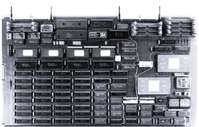
Development support is available through the WE 321DS Microprocessor Development System. The development system is a powerful development tool that can expedite the integration of hardware and software into a finished application. It permits the debugging of hardware and software to occur in parallel. The development system components include the WE 321AP Microprocessor Analysis Pod, the WE 321SD Development Software Programs, a UNIX System Host, and a logic analyzer. The modular design of the development system enables the user to configure the system for maximum productivity from initial hardware debug through the final stage of hardware and software integration. The WE 321AP Microprocessor Analysis Pod is shown on Figure 1-2.
Prototyping and performance evaluation support is available through the WE 321EB Microprocessor Evaluation Board. The evaluation board is a single-board microcomputer evaluation system that provides a prototyping vehicle to evaluate the hardware and software capabilities and performance of the WE 32100 Microprocessor in an application environment. The board is supplied with a WE 32100 Microprocessor as the CPU, a WE 32101 Memory Management Unit, a WE 32102 Clock, a ROM-based monitor, read/write memory (RAM), and sockets for additional memory. Also included are address decoding circuitry, RS-232C ports, programmable parallel 110 lines, programmable interval timers, and an interrupt controller. The WE 321EB Microprocessor Evaluation Board is shown on Figure 1-3.
1.2 Architecture
The WE 32100 Microprocessor performs all the system address generation, control, memory access, and processing functions required in a 32-bit microcomputer system. Execution speed is enhanced by its unique pipelined architecture. Using this architecture, the microprocessor overlaps the execution of instructions while tracking each separately. In addition, as each instruction is fetched from memory it is cached in an internal instruction cache, resulting in even greater operating efficiency.
The CPU utilizes a combination of address and data strobes and interface and control signals to provide the bus protocol required for efficient transfer of data. The protocol facilitates interfacing to commercial memories and peripherals, as well as providing wait-state generation for handshaking with slow peripherals. In addition, the CPU also provides special coprocessor signals for a high throughput coprocessing environment.
.,
.
•• "IS' __ ,
.,
[image:26.483.98.435.319.534.2].... ., 0 .... '
Figure 1-2. WE 321AP Microprocessor Analysis Pod
Figure 1-3. WE 321EB Microprocessor Evaluation Board
INTRODUCTION
INTRODUCTION Instruction Set
1.3 Instruction Set
The WE 32100 Microprocessor supports a powerful instruction set that includes standard data transfer, arithmetic, and logical operations for microprocessors, plus several unique operations. Its many program control instructions (branch, jump, return) provide flexibility for altering the sequence of execution. Other instructions are designed to aid in process switching for operating systems by manipulating the context of the processor with a minimum of code. In addition, special coprocessor instructions are included in the
instruction set to implement a high-speed interface with special purpose coprocessors planned for the WE 32100 Microprocessor.
Eighteen addressing modes are provided that include special high-level language support modes such as frame pointer short offset and argument pointer short offset. These modes are designed for referring to local variables of high-level functions and function arguments.
Chapter 3. INSTRUCTION SET AND ADDRESSING MODES contains a detailed description of the WE 32100 Microprocessor Instruction Set.
1.4
Operating System Support
The WE 32100 Microprocessor is designed for high-level language and operating system support. To aid in the design of process-oriented systems, it provides:
• four execution privilege levels: kernel, executive, supervisor, and user • flexible transfer of execution control between privilege levels
• capability to have the operating system contained within the address space of every process
• support of explicit process switching by a scheduler
• implicit switching of processes through the interrupt structure
• layered exception handling structure, with different mechanisms used for different exceptions.
The processor groups all of the switchable process context into a compact area in memory called the process control block. This feature, plus the use of the special operating system instructions and microsequences, provides the programmer with an excellent tool for the creation and support of process-oriented systems.
INTRODUCTION
Software Generation Programs
1.5 Software Generation Programs
The WE 321SG Software Generation Programs (SGP) is a package of support tools used to create and test programs for the WE 32100 Microprocessor. The SGP runs under the UNIX Operating System and uses many features of the UNIX System shell. The SGP allows the programmer to generate code in the high-level C language and test programs at the source leveL This improves productivity and program accuracy by freeing
programmers from the details of the hardware architecture associated with assembly language programming.
The SGP contains a C compiler that converts C language programs into assembly language programs. The assembly language programs are ultimately translated into object files by the SGP assembler for the WE 32100 Microprocessor and link-edited into executable load modules by the link editor (also contained in the SGP). Each of these tools preserves all symbolic information necessary for meaningful symbolic testing at the source level. The SGP also provides a variety of utilities that read and manipulate object files.
Chapter 2
CHAPTER 2. ARCHITECTURE & BUS OPERATION CONTENTS
2. WE 32100 MICROPROCESSOR OVERVIEW ... 2-1 2.1 USER REGISTERS... 2-3 2. J.l General-Purpose Registers
(rO-r8) ... 2-4 2.1.2 Frame Pointer ... 2-4 2.1.3 Argument Pointer ... 2-4 2.1.4 Processor Status Word ... 2-4 2.1.5 Stack Pointer ... 2-7 2.1.6 Process Control Block Pointer.... 2-7 2.1. 7 Interrupt Stack Pointer ... 2-7 2.1.8 Program Counter ... ... 2-8 2.2 DATA HANDLING ... 2-8 2.2.1 Data Types ... 2-8 2.2.2 Data in Memory ... 2-10 2.2.3 Memory Management... 2·10 2.3 SIGNAL SAMPLING
POINTS ... 2-11 2.4 READ AND WRITE
OPERATIONS ... 2-12 2.4.1 Read Transaction
Using SRDY ... 2-13 2.4.2 Read Transaction
Using DTACK ... 2-15 2.4.3 Read Transaction With Wait
Cycle Using SRDY ... 2-16 2.4.4 Read Transaction With Two
Wait Cycles Using DTACK ... 2-17 2.4.5 Write Transaction
Using SRDY... 2·18 2.4.6 Write Transaction
Using DTACK ... 2-18 2.4.7 Write Transaction With
Wait Cycle Using SRDY ... 2-18 2.4.8 Write Transaction With Wait
Cycle Using DTACK ... 2-22 2.5 READ INTERLOCKED
OPERATION ... 2-22 2.6 BLOCKFETCH OPERATION .... 2-25 2.6.1 Blockfetch Transaction
Using SRDY... 2-25 2.6.2 Blockfetch Transaction
Using DTACK ... 2-27 2.6.3 B10ckfetch Transaction Using
DTACK With Wait
Cycle On Second Word ... 2-28
2.6.4 Blockfetch Transaction Using SRDY With Wait
Cycles On Both Words ... 2-29 2.7 BUS EXCEPTIONS ... 2-30 2.7.1 Faults ... 2-30 Fault With SRDY... 2-32 Fault After DTACK ... 2·33 2.7.2 Retry ... 2-34 2.7.3 Relinquish and Retry ... 2-34 2.8 BLOCKFETCH SPECIAL
CASES ... 2-37 2.8.1 Fault on First Word of
Blockfetch With Status
Code Other Than Prefetch ... 2-37 2.8.2 Fault on First Word
of Blockfetch With
Status of Prefetch ... 2·37 2.8.3 Retry on First Word of
Blockfetch ... 2-37 2.8.4 Retry on Second Word of
Blockfetch ... 2-37 2.8.5 Relinquish and Retry of
Blockfetch ... 2·42 2.9 INTERRUPTS ... 2·42 2.9.1 Interrupt Acknowledge ... 2-42 2.9.2 Auto-vector Interrupt.. ... 2-45 2.9.3 Nonmaskable Interrupt.. ... 2-45 2.9.4 Quick Interrupt ... 2-48 2.10 BUS ARBITRATION ... 2-48 2.10.1 Bus Request During a
Bus Transaction ... ... 2-48 2.1 0.2 DMA Operation ... 2-51 2.11 RESET ... 2-52 2.11.1 System Reset ... 2-52 2.11.2 Internal Reset ... 2·52 2.11.3 Reset Sequence ... 2-54 2.12 ABORTED MEMORY
ACCESSES... 2-54 2.12.1 Aborted Access on PC
Discontinuity With
Instruction Cache Hit... 2-55 2.12.2 Alignment Fault Bus Activity ... 2·56 2.13 SINGLE-STEP OPERATION ... 2-57 2.14 COPROCESSOR
CONTENTS
2.14.1 Coprocessor Broadcast ... 2-58 2.14.2 Coprocessor Operand Fetch ... 2-63 2.14.3 Coprocessor Status Fetch ... 2-64 2.14.4 Coprocessor Data Write ... 2-65 2.15 EXCEPTIONAL
CONDITIONS ... 2-66 2.16 TRACE MECHANISM ... 2-69 2.17 PIN ASSIGNMENTS ... 2-70
2.18 MICROPROCESSOR OPERATING
REQUIREMENTS ... 2-83 2.18.1 Electrical Requirements ... 2-84 2.18.2 Clocking Requirements ... 2-85 2.18.3 Thermal Requirements ... 2-85 2.19 Supplementary Protocol
ARCHITECTURE & BUS OPERATION Overview
2. WE 32100 MICROPROCESSOR OVERVIEW
The WE 32100 Microprocessor is the first 32-bit microprocessor with separate 32-bit address and data buses. Using either physical or virtual addresses, the 32-bit address bus can access over four billion (232) bytes of system memory or peripherals. Data is read or written over the 32-bit bidirectional data bus in either byte (8-bit), halfword (16-bit), or word (32-bit) lengths and is processed internally over 32-bit internal data paths.
The execution speed of the microprocessor is enhanced by an internal instruction queue and an internal instruction cache that store prefetched instructions. Also, the microprocessor's extensive use of pipelining allows overlapping of the execution of instructions while tracking each one individually. Should a fault or interrupt occur during instruction execution, the instruction that caused it can be easily determined and execution restarted. This feature is essential for systems with demand-paged memory management.
Using a group of address and data strobes and interface and control signals, the microprocessor controls information flow over the address and data buses. These signals provide the timing required for transfer of data and facilitate interfacing to commercial memories and peripherals. The microprocessor also accommodates wait-state generation to allow handshaking with slow peripherals.
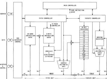
The WE 32100 Microprocessor consists of the four major sections shown on Figure 2-1. These are the main controller, the fetch unit, the execute unit, and the bus interface control. The main controller is responsible for acquiring and decoding instruction opcodes and directing the action of the fetch and execute controllers as the specified instruction is executed. The main controller also has the responsibility of responding to and directing the handling of interrupts and exception conditions.
The fetch unit handles the instruction stream and performs memory-based operand accesses. It consists of a fetch controller, an instruction cache, an instruction queue, an immediate and displacement extractor, and an address arithmetic unit (AAU). The fetch controller directs the action of the elements in the fetch unit. The instruction cache is a 64 by 32-bit on-chip cache which is used to increase the microprocessor's performance by reducing external memory reads for instruction fetches. When an instruction fetch from memory occurs, instruction data is placed in the cache and in the instruction queue. If
that instruction data is needed again, it is fetched from the cache rather than from external memory, which improves performance. The instruction queue is an 8-byte first-in-first-out queue that stores prefetched instructions. Instructions are taken from the queue for execution, and the fetch controller fills it asynchronously with respect to instruction execution. The immediate and displacement extractor provides address calculation data to the AAU for its use in calculating 32-bit addresses.
The execute unit performs all arithmetic and logic operations, performs all shift and rotate operations, and computes condition flags. It consists of:
ARCHITECTURE & BUS OPERATION
Overview
• sixteen 32-bit registers that are user-accessible and include:
o
nine general-purpose registers (rO-r8)o
seven dedicated registers (r9-r15)• working registers that are used exclusively by the microprocessor and.are not user-accessible
• a 33-bit ALU that performs arithmetic operations on 32-bit data, with an extra bit that is used whenever an operation requires a carry or borrow beyond 32 bits.
The bus interface control provides all the strobes and control signals necessary to implement the interface with peripherals.
The WE 32100 Microprocessor pin assignments are summarized in 2.17 Pin Assignments.
,
-I
MAIN CONTROLLERj
I
I
FROM INSTRUCTION~
QUEUEH
FETCH CONTROLLERI
EXECUTE CONTROLLERJ
ADDRESS
1
f
CONTROLLER TO MAIN32-8IT
REGISTERS
rO '
-DATA
B-BYTE r1
S4-WORD
r2
INSTRUCTION
H9-'>
INSTRUCTION r-r3
CACHE QUEUE WORKING
~ BUS r' REGISTERS
INTERFACE r5
~ CONTROL r6
1
r7 rB FPI
I-r:r
APIMMEDIATE I - - PSW
~Iif}
G SP LOGIC
DISPLACEMENT PCBP UNIT
EXTRACTOR ISP
rJ
INTERFAC
G
CONTROL E~
PC
\ ADDRESS
j
ARITHMETIC
UNIT
32 32 32 32
32 ABUS JO,. 32
~
" - - - 1+----· - - - FETCH UNIT - - -
--'*'
32 32
CBUS
[image:35.469.53.410.253.516.2]ARCHITECTURE & BUS OPERATION
User Registers
2.1 USER REGISTERS
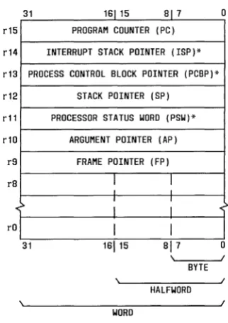
Figure 2-2 shows the programming model for the microprocessor's sixteen 32-bit registers (rO-r15). This register set is designed for efficient support of high-level language program execution. All of these registers, except for the program counter (r15) and the processor status word (r11), may be accessed in any addressing mode. The processor status word (r1l), process control block pointer (r13), and interrupt stack pointer (r14) are privileged registers. These may be read at any time, but may be written only when the microprocessor is in kernel mode (i.e., the operating system is in control). The other registers may be read or written in any of the four execution levels.
31 16J 15 SI7 0
r15 PROGRAM COUNTER (PC) r14 INTERRUPT STACK POINTER (ISP)* r13 PROCESS CONTROL SLOCK POINTER (PCSP)* r12 STACK POINTER (SP)
r1 1 PROCESSOR STATUS WORO (PSW)* r10 ARGUMENT POINTER (AP)
r9 FRAME POINTER (FP)
rB I I
;
;
"irO 1 1
31 16115 BI7 o
''--'''s y""T:-E--' HALFWORD WORD
* KERNEL LEVEL PRIVILEGED
[image:36.470.163.324.230.458.2]ARCHITECTURE & BUS OPERATION General-Purpose Registers
2.1.1 General-Purpose Registers (rO-rS)
The nine general-purpose registers may be used for high-speed accumulation, for addressing, or for temporary data storage. The first three registers (rO-r2) are the microprocessor's scratch registers. These three registers are used by the C compiler to store temporary values during expression evaluation. They also pass and return specific values during procedure calls. For example, rO should always be used to return the value of a procedure. If a floating point double value is returned from a procedure, it is stored in rO and rl. If a procedure returns a structure, then the pointer to that structure should be returned to r2. In addition, registers rO-r2 are implicitly used by the data transfer instructions MOVBLW (move block of words), STRCPY (string copy), and STREND (string end) and also by the MVERNO (move version number), INTACK (interrupt acknowledge), ENBVJMP (enable virtual pin and jump), DISVJMP (disable virtual pin and jump), GATE (system-cal!), and CALLPS (call process) operating system
instructions.
2.1.2 Frame Pointer
The frame pointer (FP), r9, points to the beginning location in the stack of a function's local variables. It is affected implicitly only by the save register (SAVE) and the restore register (RESTORE) instructions.
2.1.3 Argument Pointer
The argument pointer (AP), rIO, points to the beginning location in the stack where a set of arguments for a function has been pushed. The AP is affected implicitly only by the procedure call (CALL) and return (RET) instructions.
2.1.4 Processor Status Word
The processor status word (PSW), r1l, contains status information about the
microprocessor and the current process. It is divided into 14 fields, as shown on Figure 2-3. Although the PSW is a privileged register, the microprocessor may alter some of its fields at any execution level. Most instructions alter the N, Z, V, and C bits (condition flags) in the PSW. In general, the PSW changes as a whole only when a process switch occurs. The final values of the PSW bits are based on the result of the last calculation and are latched into the PSW at the end of the instruction. The PSW may not be referenced in some addressing modes.
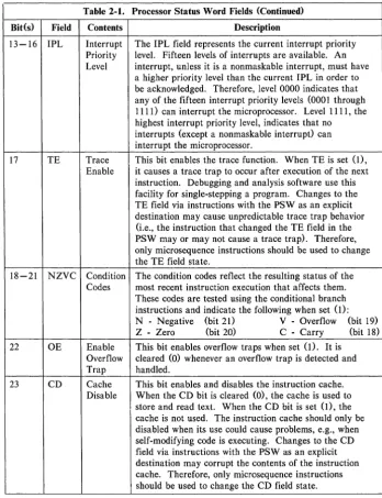
Bit(s) Field
0-1 ET
2 TM
3-6 ISC
7-8 RI
9-10 PM
11-12 CM
ARCHITECTURE & BUS OPERATION
Processor Status Word
Table 2-1. Processor Status Word Fields
Contents Description
Exception This read-only field indicates the type of exception Type generated during operations and is interpreted as:
Code Description
Bit I Bit 0
0 0 On Reset Exception
0 1 On Process Exception
1 0 On Stack Exception
I I On Normal Exception
(See 2.12 Exceptional Conditions,)
Trace The read-only TM field enables masking of a trace trap. Mask This bit masks the trace enable (TE) bit for the duration
of one instruction to avoid a trace trap. The TM bit is set (1) at the beginning of every instruction and cleared
(0) as part of every microsequence that performs a context switch or a return from gate (RETG) or when any fault or interrupt is detected and responded to. Internal This 4-bit code distinguishes between exceptions of the State same exception type. The ISC is a read-only field. (See Code 2.15 Exceptional Conditions,)
Register- These bits control the context switching strategy. The I Initial bit (bit 7) determines if a process executes from initial Context or intermediate saved context. The R bit (bit 8, read
only) determines if the registers of a process should be saved during a process switch. It also controls block moves to change map information. (See Chapter 4,) Previous This field defines the previous execution level. The code Execution is interpreted as:
Level Code Description
Bit 10 Bit 9
0 0 Kernel level
0 1 Executive level
1 0 Supervisor level
1 1 User level
Current This field defines the current execution level. The code Execution for bits II and 12 is interpreted in the same manner as Level that of bits 9 and 10 of the PM code, respectively.
[image:38.468.77.416.74.542.2]ARCHITECTURE & BUS OPERATION
[image:39.472.45.394.78.532.2]Processor Status Word
Table 2-1. Processor Status Word Fields (Continued) Bit(s) Field Contents Description
13-16 IPL Interrupt The IPL field represents the current interrupt priority Priority level. Fifteen levels of interrupts are available. An Level interrupt, unless it is a nonmaskable interrupt, must have
a higher priority level than the current IPL in order to be acknowledged. Therefore, level 0000 indicates that any of the fifteen interrupt priority levels (0001 through 1111) can interrupt the microprocessor. Level 1111, the highest interrupt priority level, indicates that no interrupts (except a nonmaskable interrupt) can interrupt the microprocessor.
17 TE Trace This bit enables the trace function. When TE is set (1), Enable it causes a trace trap to occur after execution of the next
instruction. Debugging and analysis software use this facility for single-stepping a program. Changes to the TE field via instructions with the PSW as an explicit destination may cause unpredictable trace trap behavior
(i.e., the instruction that changed the TE field in the PSW mayor may not cause a trace trap). Therefore, only microsequence instructions should be used to change the TE field state.
18-21 NZVC Condition The condition codes reflect the resulting status of the Codes most recent instruction execution that affects them.
These codes are tested using the conditional branch instructions and indicate the following when set (1); N - Negative (bit 21) V - Overflow (bit 19) Z - Zero (bit 20) C - Carry (bit 18) 22 OE Enable This bit enables overflow traps when set (1). It is
Overflow cleared (0) whenever an overflow trap is detected and Trap handled.
23 CD Cache This bit enables and disables the instruction cache. Disable When the CD bit is cleared (0), the cache is used to
ARCHITECTURE & BUS OPERATION
Interrupt Stack Pointer
Table 2-1. Processor Status Word Fields (Continued) Bit(s) Field Contents Description
24 QIE Quick- The QIE enables and disables the quick-interrupt Interrupt facility. If QIE is set ([), an interrupt is handled via the Enable quick-interrupt sequence. If QIE is cleared (0), the
interrupt causes a process switch (full-interrupt sequence).
25 CFD Cache When set (I), bit 25 disables instruction cache flushing Flush (emptying of the cache's contents) when a new process is Disable loaded via the XSWITCH_TWO microsequence (see
4.8.4 Microsequences). When cleared (0), the contents of the cache are flushed when a new process is loaded via the XSWITCH TWO microsequence.
26-31 Unused These bits are not used and must always be cleared (0).
2.1.5 Stack Pointer
The stack pointer (SP), rl2, contains the current 32-bit address of the top of the execution stack; i.e., the memory address of the next item to be stored on (pushed on) the stack or the last item retrieved (popped) from the stack. The stack pointer and the related instructions implement a LIFO Oast-in-first-out) queue that supports efficient subroutine linkage and local variable storage.
2.1.6 Process Control Block Pointer
The process control block pointer (peBP), rl3, points to the starting address of the process control block for the current process. The process control block is a data structure in external memory that contains the hardware context of a process when the process is not running. This context consists of the initial and current contents of the processor status word, program counter, and stack pointer; the last contents of registers rO through rlO; boundaries for an execution stack; and block move specifications (and possibly memory specifications) for the process. The PCBP may only be written when the microprocessor is in kernel mode.
2.1.7 Interrupt Stack Pointer
ARCHITECTURE & BUS OPERATION Program Counter
2.1.8 Program Counter
The program counter (PC), r15, contains the 32-bit memory address of the instruction being executed or, upon completion, the starting address of the next instruction to be executed. The PC may not be referenced in some addressing modes and is usually implicitly referenced by all program control instructions and all function calls and returns.
2.2 DATA HANDLING
All operations within the microprocessor are performed on 32-bit quantities, but data may be read or written as a byte, halfword, or word. Bits are numbered from right to left, starting at 0, and are right-adjusted on the address/data bus. The microprocessor automatically extends a byte or halfword to 32 bits before performing an operation. Zeros fill the high-order bits for unsigned operations, while the sign bit (bit 7 for bytes, bit 15 for halfwords) fills the high-order bits for signed operations. See Chapter 3 for a detailed description of data handling.
2.2.1 Data Types
The WE 32100 Microprocessor supports the following integer data types: • byte
• halfword
• word
A byte is an 8-bit quantity that may appear at any address. Bits are numbered from right to left starting with 0, the least significant bit (LSB), and ending with 7, the most significant bit (MSB). (See Figure 2-4.) A halfword is a 16-bit quantity that may appear at any address that is divisible by 2. Bits are numbered from right to left starting with 0, the LSB, and ending with 15, the MSB.
A word is a 32-bit quantity. A word may appear at any address that is divisible by 4. Bits are numbered right to left starting with 0, the LSB, and ending with 31, the MSB.
BITS
BITS
BITS
ARCHITECTURE & BUS OPERATION
Data Types
7 a
Fi
MSB LSB
A. BYTE OAT A
15 81 7 a
I
t
:
t
I
MSB LSB
B. HALFWORD DATA
31
24: 23 16: 15 8: 7 a
I
l
t
t
MSB LSB
C. WORD DATA
Figure 2-4. Bit Order of Data
MSB LSB
t
t
31 24: 23 16 15 8 7 a
x : a
1 1 1 1a
1 1! D 1 X 0 0 0xl
~
~ WIDTH~
I I OFFSET BASE WORD AT ADDRESS aLEGEND:
BASEWORD ADDRESS = a OFFSET = 6 WIDTH = 9
MSB LSB
t
9t
a101 1 1 101 1011
ARCHITECTURE & BUS OPERATION
Data in Memory
2.2.2 Data in Memory
Memory locations consist of a series of 8-bit (byte) locations for storing data. Halfwords occupy two consecutive memory locations and words occupy four consecutive memory locations. Boundary restrictions apply to the starting location of halfwords and words. Halfwords may only appear at addresses divisible by 2, and words may only appear at addresses divisible by 4. The microprocessor generates a fault if these boundaries are violated.
During memory reads the memory system must provide a word of data. The memory system must ignore the two lowest address bits (ADDROO and ADDROl) and provide the word data beginning at this resulting word address.
Memory writes require that the memory system be set up in byte format, i.e., each byte must be writable independent of all other bytes. During memory writes, only the byte or bytes the CPU wants to write are to be changed. The remaining byte or bytes of the same word, if any, must not be altered. The CPU informs the memory system which byte(s) should be written based on the contents of the data size bits (DSIZEO and DSIZEl) and the lower two address bits (ADDROO and ADDROI). Table 2-2 indicates which byte(s) should be written based on the following byte addressing.
DSIZEI DSIZEO
0 0
I 0
I I
Data Byte
(Word) (Halfword)
(Byte)
•
Increasing AddressesTable 2-2. Memory Write Summary
Memory Byte<s) Written ADDROI ADDROO Byte 0 Byte 1 Byte 2
0 0 Written Written Written 0 0 Written Written Unchanged I 0 Unchanged Unchanged Written 0 0 Written Unchanged Unchanged 0 I Unchanged Written Unchanged I 0 Unchanged Unchanged Written I I Unchanged Unchanged Unchanged
Byte 3 Written Unchanged Written Unchanged Unchanged Unchanged Written
Note: For write transactions, any combination of DSIZEI-DSIZEO and ADDROI-ADDROO not indicated in the table generates an alignment fault.
2.2.3 Memory Management
ARCHITECTURE & BUS OPERATION
Signal Sampling Points
accepting virtual addresses from the microprocessor and translating them into physical addresses (the physical address of the data). Therefore, the MMU can provide a vast address space per process (over four billion bytes of virtual or physical address space).
2.3 SIGNAL SAMPLING POINTS
The WE 32100 Microprocessor utilizes two phase-shifted input clocks (CLK23 and CLK34) as depicted on Figure 2-6. The CPU samples all inputs at the points indicated on this figure. This figure can be used as a reference for the protocol diagrams in the sections that follow.
CLK23
CLK34
*
double latched Notes:ASYNCHRONOUS
SAMPLING SYNCHRONOUS POINT SAMPLING
BUSRO IPLO-IPL3 BRACK (CPU NMINT NOT MASTER) AVEC
DONE INTOPT
STOP
RfSITR
POINT
F AUL T* DA T AOO-DA T A31 RETRY*
RRREO* SRDY BLKFTCH
1. BUSRQ, BRACK, IPLO-IPL3, NMINT, AVEC, INTOPT, STOP, RESETR are sampled repetitively one CLK34 cycle apart (i.e., on every clock cycle).
2. After DTACK is asserted, FAULT, RETRY, RRREQ and BLKFTCH are sampled once at the synchronous sampling point. If FAULT, RETRY, or RRREQ are asserted prior to or at the same time as DTACK, then they are sampled once and double latched. If SRDY is asserted, then FAULT, RETRY, RRREQ and BLKFTCH are sampled once at the synchronous sampling point.
3. BLKFTCH must remain asserted until negation of data strobe (Os).
4. DSHAD is not latched and can be asserted at any time subject to the following conditions: DSHAD should only be asserted during a CPU-initiated transaction while AS is active and DTACK, SRDY, and FAULT are inactive. Unless RETRY or RRREQ is active, DSHAD should only be negated while AS is still active and DTACK, SRDY and FAULT are inactive. If RETRY or RRREQ is active, then DSHAD should be negated one cycle after AS is negated.
ARCHITECTURE & BUS OPERA nON
Read & Write Operations
The bus transactions that are described in the upcoming sections share the following attributes. The read/write (R/m output remains in its mode (high, logic 1, for read transactions and low, logic 0, for write transactions) for the entire transaction. The cycle initiate (CYCLEI) output goes active for two clock cycles at the beginning of each transaction. The CPU asserts the data ready (DRDY) output at the end of the transaction if there are no bus exceptions (fault, FAULT; retry, RETRY; or relinquish and retry (RRREQ) during the transaction.
The address bus (ADDROO-ADDR3I) is driven for the entire transaction if the CPU is operating in physical mode. If the CPU is operating in virtual mode, the CPU only drives the address bus during the first and second clock states. (One clock state is half a clock cycleJ The CPU 3-states its address bus during the third clock state so that the MMU can drive the translated physical address onto the bus.
The data size bits (DSIZEO-DSIZEI) indicate the size of the transaction (byte, halfword, word, or double word) and are driven for the entire transaction. The access status code (SASO-SAS3) is driven one clock cycle before the transaction starts and remains active for two additional cycles during the transaction. This 4-bit code indicates the type of transaction being performed. At clock state four, the access status code is changed to reflect the next operation (if the next operation is a bus transaction) or to "no operation" (if the next operation is not a bus transaction). The leading edge of CYCLEI can be used to latch the access status code.
2.4 READ AND WRITE OPERA nONS
The WE 32100 Microprocessor performs zero wait-state read and write accesses in three clock cycles. These accesses are performed in two stages. The microprocessor first outputs the address and the control signals necessary for the given operation. Once these signals have had time to settle, the data transfer takes place. All accesses are followed by a vestigial cycle to allow enough time for a memory management unit to release the shared address bus.
Two inputs that allow handshaking between the CPU and slow slave devices are provided. External devices can cause the CPU to insert wait cycles during a bus transaction through the use of the synchronous ready (SRDY) input and the data transfer acknowledge
(DTACK) input. Wait cycles prolong a bus transaction which allows slave devices more time to place data on the bus during a read transaction and more time to pick up data from the bus during a write transaction.
ARCHITECTURE & BUS OPERA nON
Read Transaction Using SRDY
In the following read and write operation descriptions, the term "asserted" means that a signal is driven to its active state either by the microprocessor (outputs) or by an external device (inputs). The term "negated" means that the signal is driven to its inactive state. A bar over a signal name (e.g., As) indicates that the signal is active low, logic O.
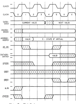
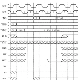
2.4.1 Read Transaction Using
SRi5Y
Figure 2-7 illustrates a read transaction with zero wait cycles (3 cycle access) using SRDY to terminate the access. The read transaction starts with the CPU driving the address bus (ADDROO-ADDR3t) and the data size outputs (DSIZEO-DSIZEt), negating the read/write (R/W) output to indicate that a read operation is being performed, and asserting the cycle initiate (CYCLEI) output at the beginning of clock state zero.
For read operations the address strobe (As) and data strobe (DS) have the same timing. The CPU latches data driven onto the data bus by the addressed device at the end of clock state four, when the CPU negates AS and DS. Data can be driven onto the bus while AS and DS are active.
The transaction illustrated on Figure 2-7 is terminated by the assertion of SRDY by the addressed device. SRDY is the acknowledgement that the addressed device is putting the data onto the data bus and that the CPU can latch the data and terminate the transaction.
SRDY is synchronously sampled at the end of clock state three.
ARCHITECTURE & BUS OPERATION
Read Transaction Using SRDY
CLK23
CLK34
SASO-SAS3
DSIZEO-DSIZEI
ADD ROO-ADDR31
DATAOO-DATA31
Riw
-Lr
~
Lr
-~
I~
~
I~
CURRENT VALID
--
,< «
-\\(
-
VALID1
-
\\
\ \
-X£l -X£l
m
-'ilL
-
~\
Note: Zero Wait Cycles.
~
Lr
~
Lr
~r
~
~
~
I~
~
[\
J
«<
NEXT VALID3 - STATE IF VIRTUAL
'11/
J VALID
:XXX :XXX
'\X :XXX :XXX :XXX :XXX
M
IX :XXX :XXX :XXX
,\
\
\
'iLL
ARCHITECTURE & BUS OPERATION Read Transaction Using
DTACK
2.4.2 Read Transaction Using DTACK
The read transaction using DTACK is identical to the read transaction using SRDY, except that the addressed device asserts DTACK to acknowledge that it is putting data on the data bus instead of SRDY (see Figure 2-8). DTACK is asynchronously sampled at the end of clock state two and is double latched to avoid metastability.
The read transaction shown on Figure 2-8 completes in three clock cycles because the CPU samples DTACK active at the end of clock state two. Upon sampling DTACK active, the CPU latches the data and terminates the transaction.
CLK23 CLK34
SASO-SAS3 DSIZEO-DSIZEI ADD ROO-ADDR31
AS,l5S
DATAOO-DATA31
Riiii
-Lr
~
J"
~
Lr
~
Lr
~
-~
~
~
~~
~
~
I~
~
-
\CURRENT VALID
<<<
NEXT VALID-<<<
-<<<
VALID)
3 - STATE IF VIRTUAL-,\\\
'III,
-VALID
XIX
XXX
-:XXX: :XXX :X\
'XXX: :XXX :XXX
m
XXX XIX XXX XIX XIX XIX
XIX
,\
\\
~7
-'ill
,\\\
'/
/ /
-Note: Zero Wait Cycles.
[image:48.472.113.372.192.542.2]ARCHITECTURE & BUS OPERATION Read Transaction With Wait Cycle Using SRDY
2.4.3 Read Transaction With Wait Cycle Using SRDY
The CPU inserts wait cycles during bus transactions if it does not sample DTACK active at the end of clock state two or SRDY active at the end of clock state three, and no bus exceptions occur. As illustrated on Figure 2-9, the CPU inserts one wait cycle because DTACK is not active at the end of clock state two and SRDY is not active at the end of clock state three. Only one wait cycle is inserted during the transaction because SRDY is active when sampled at the end of the wait cycle. The CPU then latches the data and terminates the transaction.
CLK23 CLK34
SASO-SAS3
DSIZEO-DSIZEI ADD ROO-ADDR31
DATAOO-DATA31
R/w
-J
~
J
~
Lr I\-
J
\..:.
Lr
'
----.
~
' I '
L!....J
' 3 '
~
Ir--yj'
~'5'
~
r - - - - \ X\ CURRENT VALID
<<<
NEXT VALID-<<<
--
: <<<
VALID)
3 - STATE IF VIRTUAL-\\
\ \
-
'III
-
VALID-
:XXX :XXX
:XXX :XXX
:xy
'<X :XXX :XXX :XXX
~XXX ~
:XXX
:xy
'\X:
::0..
IX
:XXX :XXX :XXX
-
,\\\
777
-'ill
\\\\'
'I I /
-ARCHITECTURE & BUS OPERATION Read Transaction With Two Wait Cycles Using
iITACK
2.4.4 Read Transaction With Two Wait Cycles Using DTACK
The CPU can insert multiple wait cycles during bus transactions, as illustrated on Figure 2-10. In this figure the CPU does not receive an acknowledge (DTACK or SRDY) for two clock cycles. Neither DTACK nor SRDY is active during clock states two and three or the first wait cycle. DTACK is sampled active in the middle of the second wait cycle, causing the termination of wait cycle generation. The CPU then latches the data and terminates the transaction.
CLK23
CLK34
SASO-SAS3
DSIZEO-DSIZEI
ADDROO-ADDR31
DATAOO-DATA31
Riw
-J
~
J
~
I f
~
J
~
I f
~
J
~
-~~
t-"i'
~''3"'
I~~
~ ~ I~~
~~
-CURRENT VALID
(<<
NEXT VALID-(<<
-<<<
VALID ) 3 - STATE IF VIRTUAL-\\
\
\'
'II/,
--
\ VALID~XXX
XXX
:XXX: :XXX:
:xy
:XXX .XXX :XXX
:XXX :XXX :XXX
:XY
\(X :XXX: :XXX :XXX
-
,\ \
\'
777/
-'I I I,
-
\\
\ \'
'II/,
ARCHITECfURE & BUS OPERATION Write Transaction Using
SiIDY
2.4.5 Write Transaction Using SRDY
During write transactions the R/w output is held low (logic 0) for the entire transaction. The CPU drives the data bus with the data to be written from clock state two until the end of the transaction. The access status code at the beginning of a write transaction is "write" (SAS3-SASO = 10lD).
Unlike read transactions where AS and DS have the same timing, the CPU asserts DS one cycle after it has asserted AS, allowing the addressed device to latch the data with either the leading or trailing edge of DS.
Figure 2-11 illustrates a write transaction with the addressed device using SRDY as the acknowledgement. By asserting SRDY the addressed device indicates to the CPU that it is ready to latch the data on the data bus. SRDY is synchronously sampled at the end of clock state three. On Figure 2-11, the CPU sampled DTACK inactive at the end of clock state two; however, it sampled SRDY active at the end of clock state three. As a result, the CPU terminates the transaction.
2.4.6 Write Transaction Using DTACK
The write transaction using DTACK is identical to the write transaction using SRDY, except that the addressed device asserts DTACK to indicate that it is ready to latch the data on the data bus. DTACK is sampled asynchronously at the end of clock state two. On Figure 2-12,the CPU samples DTACK active at this time and proceeds to terminate the transaction.
2.4.7 Write Transaction With Wait Cycle Using
SiiW
Wait cycle insertion for write transactions is similar to wait cycle insertion for read transactions. Just as in read transactions, the CPU inserts wait cycles if DTACK is not active when sampled at the end of clock state two, SRDY is not active when sampled at the end of clock state three, and no bus exceptions occur.
CLK23
CLK34
SASO-SAS3
DSIZEO-DSIZEI
ADDROO-ADDR31
DATAOO-DATA31
R/IY
-Lr
~
Lr
---""'1 0
1'1"'
~
I~
CURRENT VALID
-
-(~(
-«<
VALID )-,\ \ \
-<<<
-~XXX
YXX
X'!Y
-\\\
-.\\\
-Note: Zero wait cycles.
ARCHITECTURE & BUS OPERATION
Write Transaction With Wait Cycle Using
SillY
~
Lr
~
Lr
~~
~
1'5'
I~~
~
X1\
«<
NEXT VALID3 - STATE IF VIRTUAL
'I I lV
\\
\ \
'I I I
VALID
\X
:XXX
~XXX
:XXX :XXX
~
IX
~XXX
:XXX
:XXX
,\ \ \
'III
'Ill
ARCHITECTURE & BUS OPERATION
Write Transaction With Wait Cycle Using SRDY
CLK23
-
Lr
~
i f
~
-CLK34 ---'\
~
' 7 '
~
' 3 '
Lr
~
Lr
~-~
~
~
~
1\
SASO-SAS3 CURRENT VALID
<<<
NEXT VALIDDSIZEO-DSIZEI
ADDROO-ADDR31
DATAOO-DATA31
R/W
-<<<
-<<<
VALID)
3 - STATE IF VIRTUAL-.\\\
'Ill
-,\\\
'Ill
-<<<
VALID-XXX :-XXX X\
'XXX' :XXX :XXX
:XXX :XXX :XXX :XXX :XXX
:xxx
:XXX XXX
.\\\
'ill
-,\
\ \
-
,\\\
'/
/ /
Note: Zero wait cycles.
CLK23
CLK34
SASO-SAS3
DSIZEO-DSIZEI
ADDROO-ADDR31
DATAOO-DATA31
R/W
CYCLEI
-~
-V
~
J
I\-
,r
~
~ ~~
I~CURRENT VALID
«(
«<
<<<
VALID ),\
\ \
,\ \
\
( ( <
XXX XXX
~Xf:XXX :XXX: :XXX: :XY
\X:
.\
\
\
.\\\
'I I I.
ARCHITECTURE & BU,; OPER{][,ION
Write Transaction With Wait Cycle Usil1 SRDY
l\-
V
~
,r
l\-
V
~
v--;:;---~
r--;;-' 41'---1 1'5"
~
~NEXT VALID
3 - STATE IF VIRTUAL
I
'I I I.
!'I II
VALID
'0(
J<XX X£i
XIX'
XIX
W
'<X: :XA
IX :XXX :XXX :XXX
.\\\
m7:17
AR:HITECTURE & BUS
OPERATIO.R-Wri:e Transaction With Wait Cycle Using DTACK
ZA.S Write Transaction With Wait Cycle Using DTACK
[he write transaction shown on Figure 2-14 is another example of wait cycle insertion. In this transaction the addressed device asserts DTACK to indicate that it is ready to latch the i1ata, and that therefore, no more wait cycles are to be inserted.
N"either DTACK nor SRDY is active at its initial sampling point and, as a result, the CPU inserts a wait cycle. When the CPU samples DTACK a second time during the wait cycle, DTACK is now active. The CPU can then terminate the transaction.
Additional protocol diagrams for read and write operations are included in 2.19 Supplementary Protocol Diagrams.
2.5 READ INTERLOCKED OPERATION
Read interlocked operation consists of a memory fetch (read access) and one or more internal microprocessor operations, followed by a write access to the same memory location. Once the read access has been completed, the read interlocked operation may not be preempted other than by a reset. This prevents another process from altering data in memory which is being operated on by the current process. If a fault occurs during the read access, the read interlocked operation terminates without going through the write access.
CLK23
CLK34
SA SO-SAS3
DSIZEO-DSIZEI
ADDROO-ADDR31
DATAOO-DATA31
RiW
-Lr
~
Lr
~
-~
I~
' 7 '
~
r-:;-"
CURRENT VALID
--
«(
-
«(
VALID
)
-,\
\ \
--
l\\i
--
«(
:XXX :XXX
:yy
:XXX :XXX: :XXX
:xy
-- l\ \\
- ,\ \ \'
ARCHITECTURE & BUS OPERATION
Read Interlocked Operation
f
~
f
~
Lr
r'L
~
~
~
~
~
~
\«(
NEXT VALID3 - STATE IF VIRTUAL
/
/ / /
,///
VALID
:XXX :XXX :XXX
\X XXX :XXX :XXX :XXX
:'IJ\A
,\\\
,///
'11/
N I N
"'"
CLK23 CLK34 SASO-SAS3 DSIZEO-DSIZEI ADDROO-ADDR31 AS os OATAOO-DATA31 DTACK SRDY DRDY R/W CYCLEl I-V
l\-
f
~
V
l\-
V
I\--
r
~V
I\-
~
~
J
l\-
V
I\----, ~
' 3 ' ~ ~
0 ~
~ x
~
1'---' ' - - - '
~
I~ ~ ~ r-;-' 10
Lr--n"'
X~
' - - - ' 1'---'
READ INTERLOCKED READ INTERLOCKED
_\ «
NEXT VALID-, <
<<
-
1I-.
t"
-
,( «
VALID ) 3 - STATE IF VIRTUAL-
:«
< VALID ) 3 - STATE IF VIRTUAL1.\ \ \
'11/
-
,\
\\
'11/
1.\ \\
'I I /
1.\ \ \ 'I II-VALID XXX :XXX ~
ill
VALID-'
XXX
W\X
0A
XXX
XIX
0CO(
0:
X XXX
W\X
()QXXX
XIX
\;\IX
XXX :J\M
~XXX::XXX :XXX :XXX: (XXX (XM
(X
X
~XXX ~XXXW\X W\X
:xf.x
XXX KXXX
KXXX
ID (XM ::XM
~XXX:XM:
KxM
t(
X KXXX,
oo:x
::iJ:L
~ ~~
-
'II I
ht\\\
.\\
\
'I I I,
-h
t\\\
r
I I INotes:
I. Number of cycles between the read transaction and write transaction is four for swap word interlocked (SW APWI) and six for swap halfword interlocked (SW APHO and swap byte interlocked (SW APBO instructions.
2. Zero wait cycles.
~>
IE
1:1:1Q-("'l ;'=
;-:=i
:::!.t"'i g("'l ~..., Q-C: 01:1:1 16t"'i a~o·
t:I:IARCHITECTURE & BUS OPERATION
Blockfetch Transaction Using SRDY
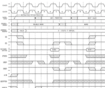
2.6 BLOCK FETCH OPERATION
The CPU can fetch two words of instruction code in one bus transaction via a blockfetch operation. The CPU generates one address, and the memory provides two words of instruction code. This reduces the number of cycles that it takes to fetch two words. The CPU starts the transaction with the DSIZE of double word, which indicates that it is ready to perform a blockfetch.
If the memory is designed to handle blockfetch, it will respond with the blockfetch (BLKFTCH) signal and an acknowledge signal, either SROY or OTACK.
2.6.1 Blockfetch Transaction Using SRDY
After the memory issues BLKFTCH and SROY, the CPU latches the data being sourced by the memory during clock state four, removes OS, and keeps AS in the active state. One cycle later the CPU reissues OS and is ready to latch the second word.
The memory drives the data bus with the second word and a SROY. The CPU samples the SROY at the end of clock state seven, then latches