ISSN (e): 2250-3021, ISSN (p): 2278-8719
Vol. 04, Issue 08 (August. 2014), ||V3|| PP 60-65
Ga Adlayer Coverage and Surface Morphology Evolution during
GaN Growth by Plasma-assisted Molecular Beam Epitaxy
Liang Pang
Department of Electrical and Computer Engineering, University of Illinois at Urbana-Champaign, IL 61801, US
Abstract: - Ga adlayer coverage and surface morphology evolution during GaN grown by PAMBE are studied on an atomic scale. Ga adlayer coverage, which is closely dependent on the Ga/N flux ratios, is found to be a very important factor in determining the surface morphology. A laterally contracted Ga bilayer is able to stabilize the GaN surface to produce the minimum pit density. Such an energetically favorable adlayer can only be achieved under certain Ga/N ratio, which is calculated from the kinetic rates of Ga adsorption and desorption.
Keywords: -Ga adlayer coverage; surface morphology; Ga/N ratio; Plasma assisted molecular beam epitaxy
I. INTRODUCTION
Due to many favorable electronic properties such as high critical breakdown field and high saturation electron velocity, GaN has become a very promising candidate material for high-frequency, high-power, and high-temperature electronics [1-7]. However, due to the lack of suitable substrate for GaN epitaxial growth, GaN crystal quality becomes the bottleneck to limit the device performance [8]. The relatively poor morphology of GaN films by current growth methods fuels great efforts to optimizethe GaN epitaxy in order to produce the excellent film quality. One important step is to understand the surface structure and growth mechanism on an atomic scale [9]. In this study, the Ga surface coverage during plasma-assisted molecular beam epitaxy (PAMBE) of GaNis carefully reviewed. We systematically investigate the surface morphology under various Ga/N flux ratios, and verify that a Ga adlayer with a total coverage of about 2.5 monolayers (ML) is the most energetically favorable surface structure forGaN, resulting in a high adatom diffusion rate and a planarized morphology [2]. The kinetic process of Ga adsorption and desorption is studied and the critical Ga incident flux under a certain N flux is obtained in order to produce the optimized Ga/N flux ratio.
II. EXPERIMENTAL RESULTS
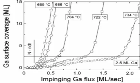
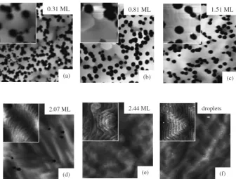
G. Koblmulleret.al.measured the Ga surface coverage as a function of impinging Ga flux at a constant N flux [10]. The Ga flux is varied to create the growth conditions from N-rich to Ga-rich and ultimately to Ga droplets, as shown in Fig. 1.Under N-rich conditions, very small adsorbed Ga coverage is observed, since the impinging Ga atoms are almost entirely depleted by the N atoms [11]. In Ga-rich intermediate stage, the Ga surface coverage increases continuously with Ga flux from 0 to around 2.5ML. This maximum 2.5ML adlayer coverage, which is referred to as a Ga bilayer structure,is verified to be the saturated adlayer coverage independent of the growth time. Further increase in the Ga flux causesthe accumulation of Ga droplets, as indicated by the sharp increase in the Ga surface coverage. Atomic force microscopy (AFM) was employed to determine the GaN surface morphology and defects. The AFM surface morphologies after growth under different Ga fluxes are presented in Fig. 2. At near-stoichiometric condition [Fig. 2(a)], a large density of surface pit makes the surface very rough. With the increase in Ga flux [Fig. 2(b) ~ 2(d)], the surface gradually
becomes smoother, and the surface pit density decreases in a continuous manner. The smoothing of the surface and the decrease of pit density are attributed to the Ga adatom surface diffusion. Since the surface adatom mobility is higher under Ga-rich conditions, faster adatom transport facilitates the filling of the surface pit defects and planarizes the morphology [13]. Once the coverage exceeds 2ML [Fig. 2(d)], the step-flow growth is clearly observed, and atomically flat terraces with step separation of unit cell height are observed. When the flux further increases to a coverage of 2.44ML [Fig. 2(e)], corresponding to the Ga bilayer structure, due to the existence of mixed-type dislocations, the stepped terraces show typical MBE-growth of spiral hillocks [14]. Finally, when the coverage exceeds the bilayer coverage, since small nano-islands consisted of Ga clusters are formed, Ga-droplet conditions are reached [Fig. 2(f)].
Fig. 2. AFM images (5×5µm2 and 1×1 µm2 for the inserts) and corresponding surface coverageataconstant N flux of 0.17ML/s and substrate temperature of 710℃. The Ga fluxes are 0.26, 0.32, 0.39, 0.46, 0.52 and
0.64ML/s for Fig.(a)~(f) respectively.
III. THEORETICAL MODELING
Studies have shown that the symmetry of GaNsurface reconstruction changes during MBE growth. Under N-rich conditions, a 2×2 N adatom local ordering is presented. With the increase of the Ga concentration, the symmetry changes from 2×2 to 5×5 to 4×6 to a final structure that is still under debate. Some researchers consider it to be a 2×2 Ga-adatom ordering, while others attribute it to a 1×1 Ga translation symmetry under tensile stress [15]. John E. Northrup et.al.suggestedas the result of first-principle total energy calculations that a pseudo-1×1 structure formed by a laterally contracted Ga bilayer is a more stable structure [16].
Fig. 3 shows a schematic representation of the bilayer structure on a Ga-terminated substrate. Ga layer 1 is a 1×1 surface with an in-plane Ga-Ga separation of 3.17Å. Layer 0 has a reduced in-plane Ga-Ga separation that is closer to a typical Ga-Ga spacing in bulk Ga (2.7Å) [17]. The reduced Ga-Ga spacing causes an energy reduction, making the laterally contracted bilayer structure more energetically favorable. It has been determined that the activation energy for Ga desorption under a Ga-rich growth condition is very similar to the activation energy for metallic Ga evaporation [18], indicating that removing a Ga atom from the top of Ga bilayer is similar to that of removing an atom from bulk Ga, a verification of the bulk-like nature of the top Ga layer.
To provethat the Ga bilayer structure produces the lowest energy, the total energy calculations are employed to determine the energy difference betweensurface structures [16]:
∆𝐸 = ∆𝐸 𝐺𝑎 − 𝑟𝑖𝑐ℎ + ∆𝑛𝑁− ∆𝑛𝐺𝑎 (𝜇𝐺𝑎 − 𝜇𝐺𝑎𝑏𝑢𝑙𝑘) (1) where ∆𝑛𝑁 and ∆𝑛𝐺𝑎 are the differences
in the total numbers of N and Ga atoms per unit area, ∆𝐸 𝐺𝑎 − 𝑟𝑖𝑐ℎ is the energy difference under Ga-rich conditions, µGa and µGa_bulk are the energies per atom of Ga in a specific surface structure and bulk Ga,
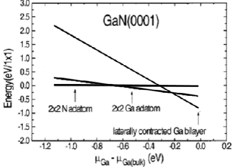
respectively. Eq. (1) shows that the energy difference in different structures is linearly dependent on the Ga chemical potential in these structures. The relative energyresulted from Eq. (1) for 2×2 N-adatomadayer, 2×2 Ga-adatomadlayerand the laterally contracted Ga bilayer are shown in Fig. 4.The 2×2 N-adatomadlayer has the lowest energy under N-rich conditions. The 2×2 Ga-adatom structure becomes more energetically favorable when the Ga chemical potential increases towards that of bulk Ga, i.e. when approaching more Ga-rich conditions. In Ga-rich limit, laterally contracted Ga bilayer forms the most stable structure, whose energy is about 0.35eV/1×1 smaller than the 2×2 Ga-adatomadlayer and 0.75eV/1×1 smaller than the 2×2 N-adatomadlayer.
Fig. 4.Relative surface energy of different structures as a function of Ga chemical potential.
IV. GA ADSORPTION AND DESORPTION DURING GROWTH
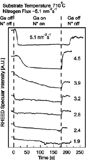
Fig. 5. RHEED intensity transients during GaN growthat constant N flux of 5.1nm-2s-1 and substrate temperature of 710℃. The Ga flux varies from 1.9 to 5.1nm-2s-1.
The growth dynamics can be described by kinetic equations. The accumulation of Ga atoms during growth follows:
𝑑 𝑛𝐺𝑎
𝑑𝑡 = (𝜎𝑎
𝐺𝑎 − 𝜎
𝑑𝐺𝑎 − 𝜎𝑎𝑁+ 𝜎𝑑𝑁) (2)
and the desorption of Ga atoms after the fluxes are interrupted follows:
𝑑 𝑛𝐺𝑎
𝑑𝑡 = −𝜎𝑑
𝐺𝑎
(3)
where𝜎𝑎𝑁 is the rate per unit area at which atomic nitrogen is incorporated, 𝜎𝑑𝑁 is the rate of nitrogen atoms lost
from the crystal due to decomposition, which is assumed to be zero since GaNdecomposition is negligible during the growth. It should also be noted that 𝜎𝑎𝐺𝑎, which represents the Ga adsorption rate, also approximates
the incident flux, since the sticking coefficient of Ga is generally unity [21]. The total adsorption and desorption time can be derived from Eq. (2) and (3) as:
𝑡𝑎=
𝑑𝑛𝐺𝑎
𝜎𝑎𝐺𝑎−𝜎𝑑𝐺𝑎−𝜎𝑎𝑁
𝑛
0 (4)
𝑡𝑑 = 𝑑 𝑛𝐺𝑎
−𝜎𝑑𝐺𝑎 0
𝑛 (5)
Thus, the relationship between 𝜎𝑎𝐺𝑎, 𝜎𝑑𝐺𝑎and 𝜎𝑎𝑁 can be obtained by taking the derivatives and equating through
the common term dn as:
𝜎𝑎𝐺𝑎 = 𝜎𝑑𝐺𝑎 𝑑 𝑡𝑑 𝑡𝑑
𝑎+ (𝜎𝑑
𝐺𝑎 + 𝜎
𝑎𝑁) (6)
The quantity dtd/dta is the slope of the desorption time with respect to the adsorption time. At a fixed substrate
temperature, the Ga desorption time varies linearly with the adsorption time, as shown in Fig. 6 [19]. Such a relationship indicates that the Ga desorption flux in the accumulation regime is constant regardless of the incident flux. If we set dtd/dta to be zero, we get the definition of the critical Ga incident flux, under which
complete Ga bilayer surface coverage is achieved without any formation of Ga droplets. Its value equals the sum of 𝜎𝑑𝐺𝑎
determining the critical Ga incident fluxin the following way: 1) experimentally determine the value of dtd/dtaat
a chosen Ga incident flux; 2) useEq. (6) to calculate the constant𝜎𝑑𝐺𝑎
; 3) obtain the critical Ga incident flux as 𝜎𝑑𝐺𝑎+ 𝜎𝑎𝑁 .
Fig.6. Ga desorption time as a function of adsorption time of three different Ga incident fluxes.
V. CONCLUSION
By reviewing the quantitative study of the surface coverage and the mechanism of GaNgrowth by PAMBE, we demonstrate that the Ga adlayer coverage strongly influences the surface morphology. The increase of the Ga/N flux ratioincreases the Ga adlayer coverage in a continuous manner from 0 to 2.5ML, leading to gradual reduction of the surface pit density andplanarization ofthe surface morphology. An equilibrium laterally contracted Ga bilayer with the minimum surface pit density is verified to be the most stable surface structure, implicating that the Ga/N flux ratio should be carefully chosen to achieve that coverage. Such a ratio is optimized via the concept of the critical Ga incident flux, whichcan be determined by the kinetic rates of Ga adsorption and desorption.
REFERENCES
[1] T. P. Chow and R.Tyagi,Wide bandgap compound semiconductors for superior high-voltage unipolar power devices,IEEE Trans. Electron Devices, 41, 1994, 1481-1483.
[2] L. Pang and K. Kim, Bimodal gate-dielectric deposition for improved performance of AlGaN/GaN metal–oxide–semiconductor high-electron-mobility transistors, J. Phys. D: Appl. Phys., 45, 2012, 045105.
[3] M. A. Khan, X. Hu, A. Tarakji, G. Simin, and J. Yang, AlGaN/GaN metal-oxide-semiconductor heterostructure field-effect transistors on SiC substrates, Appl. Phys. Lett., 77, 2000, 1339–1341.
[4] L. Pang, Y. G. Lian, D. S. Kim, J. H. Lee,and K. Kim, AlGaN/GaN MOSHEMT With High-Quality Gate–SiO2 Achieved by Room-Temperature Radio Frequency Magnetron Sputtering, IEEE Trans.
Electron Devices, 59(10), 2012, 2650-2655.
[5] S. J. Pearton and F. Ren, GaN Electronics, Adv. Mater. 21, 2000, 1571-1580.
[6] L. Pang, H. C. Seo, P. Chapman, I. Adesida, and K. Kim, Breakdown Voltage Enhancement of AlGaN/GaN High-Electron-Mobility Transistors via Selective-Area Growth for Ohmic Contacts over Ion Implantation, J. Electron. Mater. 39, 2010, 499-503.
[7] L. Pang and K. Kim, Fluoride-plasma-treated bimodal-gate-oxide AlGaN/GaN MOSHEMT for normally-off operation, IEEE Power and Energy Conference at Illinois, 2013, 8-12.
[8] F. A. Marino, N. Faralli, T. Palacios, Member, IEEE, D. K. Ferry, S. M. Goodnick, and M. Saraniti, Effects of Threading Dislocations on AlGaN/GaN High-Electron Mobility Transistors, IEEE Trans. Electron Devices, 57, 2010, 353-360.
[9] X.Q. Shen, M.Shimizu, H.Okumura, F.J.Xu, B.Shen, and G.Y.Zhang, Comparison of surface morphologies in GaN films grown by rf-MBE and MOCVD on vicinal sapphire (0 0 0 1) substrates, J. Cryst. Growth, 311, 2008, 2049-2053.
[11] B. Heying, R. Averbeck, L. F. Chen, E. Haus, H. Riechert, J. S. Speck,Control of GaN surface morphologies using plasma-assisted molecular beam epitaxy, J. Appl. Phys.88, 2000, 1855-1861.
[12] G. Koblmüller, J. Brown, R. Averbeck, H. Riechert, P. Pongratx, J. S. Speck, Ga Adlayer Governed Surface Defect Evolution of (0001)GaN Films Grown by Plasma-Assisted Molecular Beam Epitaxy, Jpn. J. Appl. Phys., 44, 2005, L906.
[13] T. Zywietz, J. Neugebauer, M. Scheffler, Adatom diffusion at GaN(0001) and (000-1) surfaces, Appl. Phys. Lett. 73, 1998, 487-489.
[14] B.Heying, E. J. Tarsa, C. R. Elsass, P. Fini, S. P. DenBaars J. S. Speck, Dislocation mediated surface morphology of GaN, J. Appl. Phys. 85, 1999, 6470-6476.
[15] A. R. Smith, R. M. Feenstra, D. W. Greve, M. S. Shin, M. Skowronski, J. Neugebauer, J. E. Northrup, Reconstructions of Ga (0001) and(000-1) surfaces: Ga-rich metallic structures, J. Vac. Sci.Technol. B, 16, 1998, 2242-2249.
[16] J. E. Northrup, J.Neugebauer, R. M. Feenstra, A. R. Smith, Structure of GaN(0001): The laterally contracted Ga bilayer model, Physical Review B, 61, 2000, 9932.
[17] J. Donohue, The Structure of the Elements, Robert E. Krieger Publishing Co., Malabar, Florida, 1982. [18] P.Hacke, G. Feuillet, H. Okumura, S. Yoshida, Monitoring surface stoichiometry with the (2×2)
reconstruction during growth of hexagonal‐phase GaN by molecular beam epitaxy, Appl. Phys. Lett. 69, 1996, 2507-2509.
[19] M. McLaurin, B. Haskell, S. Nakamura, and J. S. Speck, Gallium adsorption onto (112̄0) gallium nitride surfaces, J. Appl. Phys., 96, 2004, 327-329.
[20] P.Misra, C.Boney, D.Starikov, A.Bensaoula, Gallium adlayer adsorption and desorption studies with real-time analysis by spectroscopic ellipsometry and RHEED on A-, M-, and C-plane GaN grown by PAMBE,
J. Cryst. Growth, 311, 2009, 2033-2038.