The Enabling of an Execute-In-Place
Architecture to Reduce the Embedded System
Memory Footprint and Boot Time
Tony Benavides
Intel Corporation, Folsom, CA USA Email: [email protected]
Justin Treon, Jared Hulbert and Weide Chang Flash Memory Group, Intel Corporation California State University, Sacramento USA
Department of Computer Science
Email: [email protected], [email protected], [email protected]
Abstract—Success in the embedded world revolves around two key concepts: cost effectiveness and performance. The ability for an operating system to boot quickly combined with speedy application usage at runtime is important to consumer unit adoption. The most common memory sub-system setup in cellular phone architectures today is what is called an eXecute-In-Place architecture. This type of memory sub-system defines the execution of code and data directly from NOR flash memory. An additional memory architecture of choice is called a Store and Download architecture. This is a memory sub-system where the code gets copied to RAM at boot time and executes out of the RAM. This paper explores the addition of a new memory usage model called a Balanced XIP System. By choosing to use a Balanced XIP System you will save battery life while utilizing system resources. This is important in an age where lifestyle is driven by quick data access and electronic device energy longevity. The result is a system that combines a small RAM memory requirement with a performance increase for improved targeted application and boot time execution.
I. Introduction
In the embedded industry, speed and power savings are controversial topics. Personal cellular devices need to be designed so that they are equipped to act the fastest while taking the least power.
The topic of this paper is the design and analysis of a new memory usage architecture that puts emphasis on speeding up the application boot time responsiveness. Boot time performance is also a driving factor that many mobile phone providers push to strive for to create market separation.
Existing solutions for memory architectures consist of either a Demand Paged or eXecute in Place architecture.
Both of these models vary the way that they use RAM and Non-Volatile Memory in a system.
The current eXecute-In- Place (XIP) memory model works excellent for code execution and data storage. In systems that exhibit a situation where some data cannot take advantage of the cache in order to meet a limited latency requirement it will be of a great benefit to focus on this Balanced XIP System architecture.
When using a pure Store and Download (SnD) model, the battery life decreases due to the fact that more volatile memory has to be continually refreshed. This results in a greater current consumption from the active device. This is most notable in standby modes which may change the battery life by days. This paper investigates how to architect a memory sub-system in a way that will allow for low RAM usage, fast boot time and great application responsiveness.
The memory methodology that this paper focuses on will be a Balanced XIP System. This methodology discussed further consists of a balanced medium between the two memory architectures mentioned previously, the SnD and the XIP models.
II. Related Research
The choice of a memory system implementation depends on the cellular market segment strategy targeted. For phones that are 3G based it is expected that high end systems are employed. These high end systems are envisioned as having a high speed execution bus to handle the fast multi-media streaming interface.
Likewise, for 2-2.5G systems a different memory strategy should be employed due to its change in performance elements. There could be a slower bus interface because of the less intensive processor tasks needed. Many different companies are researching different methods to interface with their own working memory solution. Research in different memory sub-systems span over hardware and software elements. The number of memory buses, processor cores, and cache types has a large influence on the architectural model used for the memory subsystem. One flaw that is prevalent in computer architectures is the fact that usually a system is designed for one typical usage model. That model which works initially in the system is not further optimized once proven to have acceptable performance. Determining what constitutes a typical application model can be a huge challenge, and, according Hennessy and Patterson [1], a classic fallacy of computer architecture. The authors contend that there is no such thing as a typical
application. This realization has pushed processor design to follow the primary goal of achieving acceptable performance over a wide range of potential tasks rather than optimizing for any one particular task. This ideology has migrated itself into the embedded memory subsystem as well.
Throughput characteristics of memory subsystems depend upon how well a given application maps to the architecture, not on how well the architecture can adapt to the problem. Knuth’s analysis of processor intensive applications reveals that most applications spend the majority of their time in a small subset of all the
instructions that comprise a given application. This leads to the 90-10 rule in which 90% percent of the execution time is spent in 10% of the program [1]. Knuth’s analysis is also applied to the software execution strategy in the designated memory environment. Thus, in order to improve performance, the focus should be on the frequently executed subset of applications that incur the most processor time. By escalating this analysis across application use cases, common candidates for throughput improvement can be grouped into cases based on RAM consumption with a vision towards developing a hardware memory sub-system that can accommodate most of these use cases. Architectures with this ability can capitalize on the performance benefits of a
customized memory footprint analysis by tuning itself to
the current system applications while maintaining the flexibility of a total memory solution.
A. Current Cellular Architectures
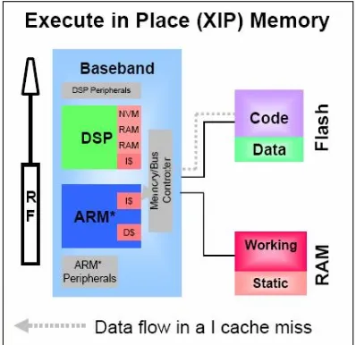
An XIP memory model consists of a system that has NOR flash and PSRAM or DRAM within it. The code is executed from the NOR flash memory. The simplicity of execution is the key to its efficient memory usage. The execution of code consists of many random reads throughout the memory. The random act of reading a NOR memory cell and its quick read speed is the basis for an XIP solution. NOR flash read speed initial accesses are ~90ns. This speed, coupled with the many random reads of flash memory equate for a good execution solution of code. Execution of system code is not sequential due to many different areas of the binary that need to be accessed in order to run in a system (ex. branch and jump instructions). Fast code execution is prevalent when you use the XIP architecture. While the NOR flash consists of code and data areas, there is also needed RAM components. RAM memory accounts for certain changing elements such as the stack, heap, and non-constant variables. As you can see, the code and read-only data are read out of the flash memory which leads to the lowest RAM density required of all the memory architectures. In a runtime environment, the RAM is primarily for application use. The density of RAM required in an XIP system is at a minimum which allows the benefit of saving power by reducing the RAM array to be refreshed. It is important to note that as a power savings addition, NOR flash memory can be turned off completely when not in use while still holding its data contents. This can be in the form of a Deep Power Mode pin on the device or a chip-select toggle.
A typical XIP image will copy “Read-Write” sections of memory into RAM at boot time. All “Read-Only” sections are kept in Flash and executed/read from. This not only includes code but also constant data elements. The remainder “Zero-Initialized” sections of RAM are used for applications and typically set to zero (scratch-pad area).
Figure 1. eXecute-In-Place diagram
Another popular architecture of choice is what is called a Store and Download (SnD) architecture. This is a memory system where the executable code is stored in Non-Volatile Memory (NVM) and copied to RAM at boot-up. At boot-up a small piece of NVM, usually within the micro-processor, runs code to copy the contents of the NVM memory (NAND or NOR) to the RAM and jumps to the RAM location. From that point the code and data are executed out of RAM. You can see that for a SnD system, large amounts of RAM are needed for the code execution. Most systems architected around a SnD model are too simple to compress the code stored in the NVM, but some systems could make use of code compression to reduce the NVM required,
In the SnD model, the code is typically stored uncompressed in the NVM. At boot up, the entire code image must be transferred from NVM to RAM before code execution can begin. Thus, as the code image grows in size the system boot-time increases. This architecture is referred to as Fully Shadowed since NVM image is shadowed in RAM.
Compared to an XIP implementation Full Shadowing creates more software overhead and complexity at boot time to copy all of the code over to the RAM. Extra RAM density is required to handle copying all of the code over to the memory. This extra RAM creates high standby power consumption due to RAM refreshing schemes. DRAM has to be continuously refreshed to retain its internal cell contents.
.
Figure 2. Store and download diagram
Demand Paged (DP) architectures can be defined as a subset of the SnD architecture. This is a method by which to minimize the RAM requirements at runtime. Code is stored compressed in NVM and will uncompress to the RAM when needed by the CPU. This is usually in the form of a page fault. Typically you will not have enough RAM in the system for all of the code. This method alleviates this issue by requesting that you have enough RAM for what is needed in the system at one time. Pages in virtual memory, not in physical memory, cause a page fault when accessed. In this method, the limited page pool is reused as different code pages are swapped in and out of main memory.
Figure 2 describes a working SnD model. In this configuration the NV storage copies over what is needed by the RAM at boot up. After this code is copied over then memory is mapped in/out as needed defined by the page fault handling scheme. The difference between this picture (SnD) and a Demand Paged environment is that with the DP you only use RAM that is needed at that time for code, along with other system RAM elements.
fault) and the time it takes for the software copy overhead (decompression).
III. Comparing Code Storage Methods
It is important to understand the current code storage methods to appreciate the Balanced XIP Architecture. The following will discuss this.
A. Compression
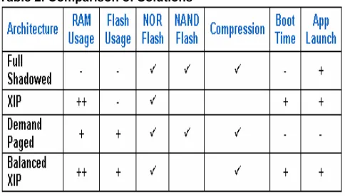
Code compression benefits embedded systems by reducing the amount of Flash required for code storage. Fully Shadowed and Demand Paged architectures can implement compression. While many Demand Paged architectures use compression, few Fully Shadowed systems use compression to simplify the system implementation. XIP architectures cannot implement compression because processors cannot execute compressed code directly.
Compressed code must be uncompressed before it can be executed. Demand Paged architectures that implement compression typically compress on a block size that is a multiple of the page size, typically 4KB. This way only a single page or a few pages need to be decompressed, when a page of code is required. For a Balanced XIP system, the code that is executed from Flash must be uncompressed; the code that is executed from RAM should be compressed in Flash to minimize Flash usage.
B. RAM And Flash Usage
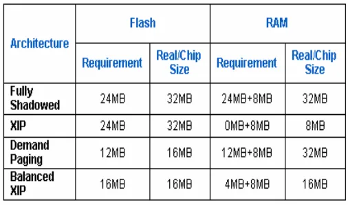
Consider a design with 24MB of executable code. A Fully Shadowed approach would use 24MB of RAM (ignoring for the moment additional RAM needed for scratchpad data) and 24MB of Flash for code. With an XIP approach, the system would use 24MB of Flash, and 0MB of RAM to store the code. A Demand Paged system, with compression (approximately 50%), would use about 12MB of Flash and some amount less than 24MB of RAM, depending on the usage model, performance requirements, and the nature of the code itself. Assuming the Demand Paged code only requires 12MB of RAM for code. A Balanced XIP system would use between 12MB and 24MB of Flash because it requires more Flash than Demand Paging and yet less than XIP. As for RAM, a Balanced XIP system would require between 0 and 12MB for code because it requires less RAM than the Demand Paging example, but more than XIP.
The Balanced XIP model gives the designer the most flexibility to create a system that can fit into standard 2n memory chip sizes. Given the example design above and
assuming the system requires 8MB of RAM for volatile data (working space), Table 1 illustrates the
Table 1. RAM and Flash Implications of Various Code Storage Architectures
memory chip sizes each architecture would require. Because of the assumed 12MB of RAM required for code in the Demand Paging example, the system would require 20MB of RAM. But, the system designer would probably design in a 32MB RAM chip and burden the cost and power budget of the design with 12MB of extra RAM. The amount of RAM required for a Demand Paging system is flexible, but the tradeoff is performance and power consumption.
Perhaps this Demand Paged design could be squeezed into a 16MB RAM chip, but with reduced performance. However, there are 4MB of Flash that is not used in the Demand Paged example. This extra Flash could be used to balance this system. Assuming a 50% compression ratio, 8MB out of the 12MB of code in RAM can be selected to be stored uncompressed/XIP in the 4MB of Flash. Therefore, 4MB of previously compressed code can be switched to 8MB of XIP/uncompressed, adding 4MB to the Flash required, but in doing so the RAM required is reduced by 8MB. Now this Balanced system fits into a reduced memory footprint of 16MB of Flash and 16MB of RAM. Thus, the Balanced XIP system has the smallest memory subsystem requirements resulting in lowest cost.
available RAM (for other system uses), minimizes application launch time and optimizes Flash usage by compressing unused or infrequently used applications pages.
C. Performance
Code performance is often a concern when choosing a code storage method. RAM read speeds are typically faster than Flash memory. NOR Flash has similar, but worse latency and bandwidth compared to RAM. While NAND Flash has very long read latency and less bandwidth than both NOR and RAM. NAND cannot be used for XIP because of these long latencies. It is often assumed that code execution from NOR Flash would be slower than code execution from RAM. However, processor instruction caches hide the differences in read speed that may exist between RAM and NOR. Paging architectures have latencies associated with interrupting the system, finding the code needed, decompressing it, and so forth. This latency occurs more often as a Demand Paged system becomes RAM constrained. Using XIP can increase the launch speed and in some cases the runtime performance when compared to a Demand Paged system because XIP/uncompressed code will not have the latencies of Demand Paged/compressed code. These factors make it difficult to judge what the performance differences of each code execution method will be.
Table 2. Comparison of Solutions
IV. Balanced XIP Architecture
Embedded system designers have a wide variety of storage methods available for their intended projects. Depending on the hardware targeted and operating/file systems used, each has its own tradeoff between read speed, write speed, and compression. The key to generating a cost effective system is to balance the storage methods defined in the previous section. After analyzing the previous cellular memory architectures, the goal is to come up with solutions that will enable fast
code execution speed while also speeding up the boot time and keeping the RAM density requirement low. The resulting investigation becomes a mixture between the DP model and the XIP model called a Balanced XIP System. The reason this method is called Balanced XIP is due to the process of taking each individual code element in the system and logically balancing its need to be
uncompressed/XIP or compressed/DP depending on performance characteristics.
It is important to detect certain bottlenecks that occur in system memory access. By locating these hotspots to RAM you can remove the bottlenecks and reduce system latency. With this architecture, the code will remain in NOR flash while selected portions of applications and constant data segments get moved over to the RAM thus decreasing bus utilization. Most normal code for executing applications does not need to be moved to RAM because of the high Instruction Cache (I$) and Data Cache (D$) hit rate [8]. Since the I$ hit rates are high, the performance becomes the same as code execution when running from DRAM. With the understanding that certain object files can be manipulated to run compressed or uncompressed, you arrive at the basis for which the method of Balanced XIP works. By targeting in on each object file you can investigate what will help system performance by putting the object in RAM (ex. data that does not keep up with D$ latency requirements), or keeping the executable in NOR flash to be run as code. This Balanced XIP interface allows the system engineer to optimize the XIP model previously discussed by being selective on what gets put in RAM and what stays uncompressed in NOR flash memory. To
implement this takes knowledge of the platform hardware and software to make it work. The process takes place from a software standpoint by interfacing with the file system through a build process, generated map file, and linker scripts.
Relating to the 90/10 rule, by recognizing the effect of being able to choose what in the system can be
Figure 3. Balanced eXecute-In-Place diagram
A. Architecture Benefits
As Amdahl’s Law states, to optimize on performance requires speeding up the time where the greatest latency is. By analyzing the hit rate and size of certain code segments you can also speed up performance, specifically during boot time. Migrating some of the constant data to high-speed RAM allows faster throughput for this data. NOR Flash and the Balanced XIP method provide the best savings of execution speed and standby power consumption in cellular platforms versus a DP model. The standby power consumption is largely due to the RAM array size. By reducing the size of the RAM array the refresh current is reduced, therefore increasing the battery life. By analyzing a typical handset usage model it can be noted that the percentage of the time is used talking on the phone is quite small compared to the percentage of time the phone remains in standby or idle mode. This is the time when the RAM will take up most of the system power.
Figure 3 describes a working Balanced XIP model. On the right side of the diagram there is the code and data which reside in flash memory. At compile time objects are chosen to reside in RAM or NVM via a compile script. The items that are accessed frequently are relocated to RAM to take advantage of the high speed access. The rest of the code is run out of NVM in a typical XIP environment.
Code executes more efficiently in a XIP system vs. a DP system because the cache makes up for any additional read discrepancy. Localized code is fed into the cache line and executed. Also, the additional software hit to uncompress the compressed code stored in the NVM adds more latency that the XIP system does not have.
Figure 3 relates how the Code Balancing system works. By selecting commonly used compressed pages in a Demand Paged implementation can be uncompressed to
reduce the overall system memory usage. The newly uncompressed files are then stored in NVM. There is an decompression latency when wanting to use these uncommonly used files in both the Demand Paged and Code Balanced implementation, but due to the codes hit ratio this will not be bad. You can see from the figure that you save on system RAM.
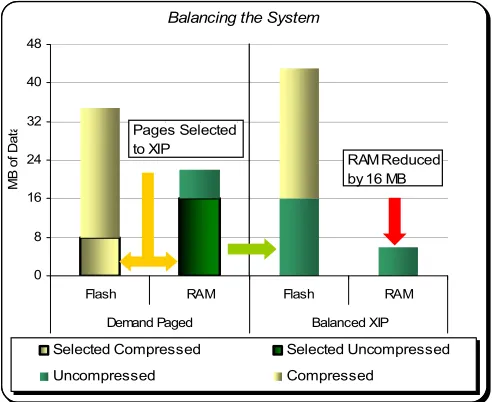
Balancing the System
0 8 16 24 32 40 48
Flash RAM Flash RAM
Demand Paged Balanced XIP
MB o
f D
a
ta
Selected Compressed Selected Uncompressed Uncompressed Compressed
Pages Selected to XIP
RAM Reduced by 16 MB
Figure 4. Analysis of balanced components
Within any memory sub-system with a compressed filing system component there is a “tug-of-war” between compression and the RAM usage. As compression of the filing system increases to reduce the size of the code stored in the flash memory, the system’s RAM requirement increases to run the decompressed code. Alternatively, when running a portion of the filing system as uncompressed the RAM requirement decreases. Uncompressed applications can be executed directly from flash without having to be buffered in the RAM. By adjusting the compressed to uncompressed code ratio, developers can purchase a smaller RAM/Flash chip combination while still achieving their performance goals. By achieving a Balanced XIP system, developers will be able to save money, increase performance, and improve end user experience.
System engineers should primarily use a Balanced XIP methodology as a tool to reduce the BOM by using the smallest and most cost effective RAM/Flash combination available. Focusing on the ideal system combination will add value by increasing application performance and boot time. By using a Balanced XIP implementation for application code, the RAM density requirement is drastically reduced.
V. Tested Configurations
experiments is an Intel PXA27x Development System. This is an embedded platform that consists of an Intel PXA270 Xscale processor, 64MB RAM, and 64MB M18 Intel Flash. For the Demand Paged version of data, a 64MB Small Page NAND device is used as the NV Storage element. The PXA270 has a 32kB internal Instruction and Data caches with each cache line consisting of 32bytes. Standard Linux build techniques were employed in this experiment. The JFFS2 and Linear XIP CRAMFS were used along with the 2.6.14 based kernel.
The test results below consists of two configurations compared (Demand Paged vs. Balanced XIP). For the Demand Paged scenario a NAND NVM was used with the JFFS2 and RAM. The Balanced XIP solution consisted of a NOR NVM with RAM using a
combination of Linear XIP CRAMFS for Read-Write data and JFFS2 for Read-Only data files.
Tables 1 and 3 refer to the data collected on the PXA27x Development Platform. Figures 3 and 4 refer to data collected on a separate PXA270 development board with 96MB of NOR flash and 64MB of RAM.
A. Test Results
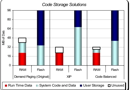
The Balanced XIP model provided the ability to decrease boot time and minimize the total memory package cost. Figure 4 outlines how the Balanced XIP solution efficiently utilizes memory space. It is easily seen that this new method uses less space than its
Demand Paged counterpart. This is due to the fact that by balancing the object components the unutilized RAM code is compressed and put into NOR flash memory. The flash portion of XIP will increase because you are putting more uncompressed data in the flash. The RAM
decreases because a great portion of the system code and data are now in flash.
Code Storage Solutions
0 16 32 48 64 80 96
RAM Flash RAM Flash RAM Flash Demand Paging (Original) XIP Code Balanced
MB o
f
D
a
ta
Run Time Data System Code and Data User Storage Unused
Figure 5. Memory usage comparison
The boot time performance also increases when the Balanced XIP method is compared to the DP. The reason that the Balanced XIP method is faster to boot stems from the process that the system follows at reset. After the reset is triggered, the processor executes code at address 0x0. For a Balanced XIP system this means that the code is executed immediately after reset.
Comparatively, the DP system boot loader must first load the kernel into RAM and decompress it before control can be passed to the kernel initialization routines. Moving the kernel and decompressing it is not required on the Balanced XIP system. As noted in Table 1, this helps the boot time by a factor of 2.2x.
Table 3. Benchmark comparisons
Technique Boot Quake Browser
Balanced
XIP 32.2 20.0 2.6
Demand
Paged 71.6 26.7 3.9
DP Slower
by
2.2X 1.3X 1.5X
When analyzing how applications launch in a Balanced XIP architecture, it can be seen that time to launch the GUI was reduced. This is because the uncompressed/XIP pages do not need to be buffered into RAM. The DP based system is primarily slower due to the demand paging overhead and page faults.
Also investigated was the launch of the application Quake and a browser used in Linux. These results, although not as apparent as the boot time numbers, helps to solidify the effects of a Balanced XIP environment. The launch time for the first person shooter Quake was 1.3x slower on the strictly DP system versus the Balanced XIP implementation. When launching the Konqueror Web Browser the DP implementation was 1.5x slower to launch versus the Balanced XIP implementation. By analyzing the differences between Demand Paged vs. Balanced XIP system it is clear to see where the reduced BOM comes from. As the engineer selectively compresses object code, she/he can balance the needs of the system by allocating what needs to be compressed and what can stay in NOR Flash memory. For example, in the Demand Paged situation there is a lot of RAM used during run time. The ability to find out what objects are being used the least and then assigning some of them to flash memory allows the RAM utilization to be increased.
VI. Balanced Execute-In-Place Filing System
XIP CRAMFS and AXFS. The Linear XIP CRAMFS decompresses files on a file-by-file basis, whereas AXFS decompresses files on a page-by-page basis offering more optimal Flash usage.
A. Linear XIP CRAMFS
Linus Torvalds originally wrote CRAMFS as a compressed read-only filing system to enable bootable floppies to install the Linux operating system on PCs. Over time, CRAMFS was modified for use in embedded systems. The Linear XIP variant adds the ability to specify each file to be stored on Flash as compressed (Demand Paged) and uncompressed (XIP). When a file is marked to be XIP all of the pages of the file are stored uncompressed contiguously in Flash. When the XIP file is requested to load, all of the page addresses are directly mapped in the memory map. Alternatively, the
compressed Demand Paged file will load each page individually when a page fault occurs. During the page fault, the handler must uncompress the page into RAM. To create a Balanced XIP file system image with Linear CRAMFS, one must determine the frequency of the usage of executables and libraries within a use case. The frequently used files can then be Executed-In-Place for the greatest RAM savings. This is not a difficult task with publicly available tools, such as RAM Usage Scan Tool (RAMUST)[10], showing which files are in the virtual memory map and which ranges within each file are mapped into the system. The Compressed Filing System Size Tool (CFSST)[11] profiles a filing system by listing the compressed and uncompressed size of all files. Employees of Wind River and others in the open source community are currently attempting to incorporate the Linear and Linear XIP patches into the mainstream Linux kernel. Linear CRAMFS and Linear XIP CRAMFS is in widespread use in Linux phones.
B. Advanced XIP Filing System
To improve the Balanced XIP solution, a new filing system was created to replace Linear XIP CRAMFS. The limitation of Linear XIP CRAMFS is that all the pages within an application are either XIP or all compressed Demand Paged. Thus, the granularity to balance the code is limited to entire application/library and not individual pages within a file. Just as in an entire code image only some files are used, within an application some pages are infrequently or never used. Therefore, storing these pages uncompressed/XIP expands the filing system image with no improvement to RAM savings.
Advanced XIP Filing System (AXFS) is a read-only filing system that has the ability to store individual pages
in a file uncompressed/XIP or compressed/Demand Paged. AXFS Filing system has a built-in profiling tool to determine which pages should be XIP and which should be Demand Paged. Pages that are infrequently called under the primary use cases are stored compressed. Pages that are often called or associated with key
applications (using the most RAM) are stored
uncompressed to remove the burden of their RAM usage from the system.
AXFS is meant a replacement filing system for SQUASHFS and CRAMFS variants. AXFS has improved compression over SQUASHFS by having variable compression block size, elimination of duplicate blocks and other compression enhancements. The filing system is broken into three storage regions. A page aligned section of uncompressed pages of memory, a section of compressed unaligned pages, and a byte aligned section containing code and data that would have actually grown larger with compression, rather than smaller. Symbolic links and other small files do not compress well so they are stored uncompress in the byte aligned region. Files in the byte aligned region may either be XIP or demand Paged into the volatile memory depending on if the filing system is stored in NOR or NAND memory.
C. Advanced XIP Filing System Generation
Creation of the AXFS filing system is similar to that of a CRAMFS filing system. Both AXFS and Linear XIP CRAMFS must be generated compressed, profiled, and then recreated on the target system as a Balanced XIP filing system. The first filing system is created completely compressed and then run on the device with profiling enabled. Profiling the system is as easy as turning on system profiling tools (Linux kernel option) and running a target-use scenario (such as turning the phone on, watching a movie, and placing/receiving a phone call). The profile data is then fed back into the filing system generation application (mkfs.axfs) and Balanced XIP filing system with compressed and uncompressed
elements will be created. Only one iteration of generating the filing system, profiling the system, and generating the new faster and less RAM intensive filing system is typically required to meet a designer’s performance and chip density goals.
code storage size. More frequently used pages (10-2000) should be selected for decompression. Pages that are cached 3-9 times should be uncompressed or compressed to reach the most cost effective RAM/Flash size while still meeting performance requirements. In other words, the compressed to uncompressed code storage ratio can be adjusted to reach the most cost effective RAM/Flash combination.
Profiling the system while booting is strongly unadvised. Many pages of code are only called during system boot and never used during other cases. By profiling the most system memory intensive applications the boot time will also be reduced. Examples of system memory intensive include placing a call, watching a movie, or browsing the web. Pages that are paged in and out frequently for the GUI and common libraries will be included in the profile and thus reduce the boot time without dramatically increasing the NVM footprint. Profiling the system is system intensive and should not be enabled on a production system since logging the page usage is system intensive.
VII. NAND Flash Memory
For years NOR flash has been the major player with regards to non-volatile memory in portable electronic devices. NAND flash’s main focus group was targeted primarily as a large-density storage medium for use in consumer devices or in other words the data memory market [4]. These devices range from solid-state storage disk drives to digital camera memory storage.
Within the past year the NAND flash memory has started to become a clear solution in areas where before, only NOR was the complete winner. Memory controllers that were once NOR-centric are now coming out with built in NAND controllers that enable the booting of NAND and the ability to handle the error correction in hardware. This is allowing NAND to enter into consumer devices where before they were only used sparingly.
Cellular phone devices are starting to focus on providing customers with data driven interfaces including MP3 players and video viewing/streaming. This is driving up the total phone density in a cellular phone. As a result, the designers of memory sub-systems are opting to design in NAND solutions where traditionally NOR was only used.
In a cellular phone, since NAND cannot be used to access random data, the best way to utilize NAND is to use the device in a Store and Download methodology. Refer to Figure 2. In this memory architecture, the NAND will be used along with SDRAM or DDR in the embedded system. With the data usage increasing per embedded device some manufactures are utilizing a blended solution using both NOR and NAND to reach performance goals while reducing the total memory
footprint. Typically the smallest combined total volatile and non-volatile memory footprint is the most cost effective solution. This is done by using the ideology of NOR for code, NAND for data.
The NAND Store and Download model would work as explained in Section 2.1. The processor would load code from the NAND to DRAM at boot-up and run the code from the DRAM. The NAND device would be used as data storage. This architecture is a little more complex than its NOR eXecute-in-Place counterpart due to the fact that you also need a special NAND controller to be able to boot from the device to get the code copied over to DRAM. There is also controversy in this architecture because some people believe that the bus between the NAND and DRAM could be snooped which would pose a security risk to the code contents. The industry is moving to MCP (Multi-Chip Package) which would house both NAND, DRAM, and the micro-Processor in a same package which could alleviate this risk.
At lower densities the initial engineering and floor costs are more involved, but at higher densities the end result could be a less expensive unit. At low densities NOR chips are cheaper than NAND, but at higher densities NAND is cheaper. The density price point at which NOR is cheaper than NAND is continually changing. The additional RAM cost for using a system that does not support NOR XIP operation should be factored into the price point.
The negative to using NAND in this type of model is that there is some extra error correction that needs to happen when using NAND memories and this correcting action can take time. The ECC can manifest itself in either a hardware or software form. The hardware form, although with additional cost, proves to be better because of its ability to act quicker than its software counterpart. In addition, using a Store and Download model tends to require more power as the DRAM tends to take more of an active role.
While the question continues as whether to go with a NOR or NAND memory architecture solution, there is no doubt that many of the cellular providers are looking at both solutions. The question still revolves around cost, speed, and ease of implementation. Many manufactures are using a blended solution using both NOR and NAND memory.
VIII. Conclusion And Future Work
phone bottom line and pass good quality, high responsive, low cost phones to consumers.
Customers will perceive a system as being slow if the boot time or application launch time is slow. Boot time along with a minimized RAM/Flash memory package are the most notable difference between a DP and Balanced XIP system.
Discussing the exploration of using the NAND flash memory as a possible alternative to NOR, it would be good to see more investigations catered at comparing the two. This could consist of both performance measuring, including Operating System overhead and filesystem manageability.
For future investigations it would be interesting to conduct this same experiment for both a WinCE Embedded system and a Real Time Operating System. The analysis of the boot time and application performance parameters for these OS’s will complete this
investigation.
This includes comparing the NAND Store and Download model with the Balanced XIP model to explore what can happen to increase performance and relieve the
complexity of adding a NAND system solution.
REFERENCES
[1] J. Hennessy and D. Patterson, Computer Architecture A Quantitative Approach, Morgan Kaufmann Publishers, Inc., 1996.
[2] Linux MTD, http://www.infradead.org, 2006.
[3] Linux Open Source Kernel, http://www.kernel.org, 2006.
[4] Steven J. Vaughan-Nichols, OS’s Battle in the Smart-Phone Market, 2003.
[5] Cliff Brake, Jeff Sutherland, Flash File systems for Embedded Linux,
http://www.linuxjournal.com/node/4678/print, 2003.
[6] MontaVista, XIP Linux Execution, http://tree.celinuxforum.org/pipermail/celinux- dev/2004November/000220.html, 2004.
[7] Howard Cheng, Eric Anderson, Mike Edgington Optimized XIP Collateral, Intel FMG Ecosystem Team, 2006.
[8] Jared Hulbert, Justin Treon, Linux Optimized XIP Collateral, Intel FMG System Analysis Team, 2006.
[9] Weide Chang, George Landis, GP-DISP: A
general purpose dynamic instruction set processor, 2004.
[10] RAMUST, RAM Usage Scan Tool, http://ramust.sourceforge.net/
[11] CFSST, Compressed File System Sizing Tool, http://cfsst.sourceforge.net/
[12] Arnold Berger,
Embedded System Design: An Introduction to Process, Tools, and Techniques, 2002
[13] Steve Heath,
Embedded System Design, 2003
Edward Tony Benavides is originally from the Bay Area and has lived in Sacramento, CA for the last 10 years.
He has received his bachelors and masters degree in electronic engineering from the California State University Sacramento and is a current PhD Candidate in electronic and computer engineering at the University of California, Davis focusing on processor/memory transactions running on many-core and memory performance optimizations.
He has been working as an embedded engineer with Intel Corporation since 1999 and currently works as an Analog Validation Engineer within the Intel Platform Memory Organization team working on validating the latest in DDR3 1333/1600 Mbps memory technologies. He has been working with Linux for the past 10 years. Besides his achievements in industry, he is a member of the IEEE and Tau-Beta-Pi engineering societies.
Weide (Willie) Chang is currently a faculty member of the computer science and computer engineering programs at California State University, Sacramento.
He received a bachelor degree in information science from Chinese Culture University, Taiwan; a master degree in computer science at the Sacramento State, and a PhD degree in computer science from New Mexico Tech. He has been awarded with numerous recognitions by IEEE. He was as an outstanding graduate student while studying at New Mexico Tech, awarded by the university; and received a research paper award from IEEE during his study. He also received an award as a distinguished alumnus from Sacramento State, a service award from Sacramento State (since joining the faculty), and two best-teacher awards from the national honor engineer society Tau Beta Pi. Besides his achievements in teaching and research, he has also been serving as a key organizer for several IEEE international conferences since 2004. His current research interests are complex-system modeling and intelligent embedded devices.
works for the CTO of the Intel Flash Memory Group managing the Linux Team trying to improve Intel NOR and NAND flash memory support for Linux. Jared has helped Intel customers optimize and port Linux on several phones currently on the market. He has also created many systems as demos for customers or internal uses such as what was probably the worlds only XIP Linux iPaq.