University of New Hampshire Scholars' Repository
Master's Theses and Capstones Student Scholarship
Spring 2019
A Miniaturized Phased Array Antenna Based on
Novel Switch Line Phase Shifter Module
Rudra Lal Timsina
University of New Hampshire, Durham
Follow this and additional works at:https://scholars.unh.edu/thesis
This Thesis is brought to you for free and open access by the Student Scholarship at University of New Hampshire Scholars' Repository. It has been accepted for inclusion in Master's Theses and Capstones by an authorized administrator of University of New Hampshire Scholars' Repository. For more information, please [email protected].
Recommended Citation
Timsina, Rudra Lal, "A Miniaturized Phased Array Antenna Based on Novel Switch Line Phase Shifter Module" (2019).Master's Theses and Capstones. 1286.
A MINIATURIZED PHASED ARRAY ANTENNA BASED ON NOVEL
SWITCH LINE PHASE SHIFTER MODULE
BY
RUDRA TIMSINA
Bachelor of Science in Electrical Engineering
University of New Hampshire, 2014
THESIS
S
ubmitted to the University of New Hampshire
in Partial Fulfillment of the
Requirements for the Degree of
MASTER OF SCIENCE
IN
ELECTRICAL ENGINEERING
Thesis Director, Dr. Richard A. Messner, Associate Professor of Electrical and Computer Engineering, University of New Hampshire
Dr. Michael J. Carter, Associate Professor of Electrical and Computer Engineering, University of New Hampshire
Dr. Wayne Smith, Senior Lecturer of Electrical and Computer Engineering, University of New Hampshire
ACKNOWLEDGEMENTS
I would like to acknowledge my advisor Professor Richard Messner for his support
and guidance to execute this project. He provided me an opportunity to carry out the
graduate level research work at the University of New Hampshire. His advice was very
influential in completing this project. I like to thank Northrop Grumman for sponsoring
this work. I would also like to thank my thesis committee members, Dr. Michael Carter
and Dr. Wayne Smith for accepting my request to be in my committee. I would like to
thank the department chair, Dr. Kent Chamberlin for guiding me through problems and
financially supporting me to attend a conference in Singapore related to this project.
I can’t help without thanking James Abare, who assisted me with antenna
fabrica-tion. I also like to thank my fellow graduate student Jean Lambert Kubwimana for his help
with test setup in the anechoic chamber and discussions with various problems while
work-ing on this project. Lastly, I would like to thank my family members, and friends who
supported me continuously throughout my education process.
TABLE OF CONTENTS
Acknowledgements ... iii
Table of Contents ... iv
List of figures ... vi
List of tables... xi
Abstract ... xii
Chapter 1: Introduction ... 1
1.1 Problem Statement ... 1
1.2 Objectives ... 3
1.3 Organization of the Thesis ... 4
Chapter 2: Background ... 6
2.1 Antenna Terminology ... 6
2.1.1 Radiation Pattern ... 6
2.1.2 Radiation Intensity ... 8
2.1.3 Beamwidth ... 8
2.1.4 Directivity... 9
2.1.5 Antenna Gain... 9
2.1.6 Antenna Efficiency ... 10
2.1.7 Bandwidth ... 10
2.1.8 Polarization... 11
2.2 Transmission Line ... 12
2.2.1 Transmission Line Types ... 12
2.2.2 Voltage Reflection Coefficient (Γ) ... 15
2.2.3 Voltage Standing Wave Ratio (VSWR) ... 16
2.2.4 Input Impedance ... 16
2.2.5 Return Loss and Insertion Loss ... 17
2.2.6 Impedance Matching ... 17
2.2.7 Scattering Parameters (s-Parameters)... 19
2.2.8 Impedance Parameters (Z-parameters) ... 21
2.3 Microstrip Antenna ... 21
2.3.1 Rectangular Patch Antenna ... 22
2.3.2 Feeding Methods ... 24
2.5 High Frequency Structural Simulator (HFSS) Background ... 31
2.5.1 Antenna Geometry ... 33
2.5.2 Boundary Conditions ... 33
2.5.3 Excitation ... 36
2.5.4 Post Processing ... 36
Chapter 3: Antenna Design and Simulation ... 38
3.1 Single Rectangular Patch Antenna ... 38
3.1.1 Design... 38
3.1.2 Simulation ... 40
3.1.3 Results ... 43
3.2 Phase shifter ... 46
3.2.1 Design... 46
3.2.2 Stub Matching ... 49
3.3 Single Antenna with Phase Shifter ... 57
3.4 Simulation Results ... 59
3.5 Corporate feed design ... 69
3.6 Phased Array Antenna ... 71
3.6.1 Design... 71
3.6.2 Simulation Results... 74
3.6.3 Mutual Coupling ... 84
3.7 Phase Control Design ... 86
Chapter 4: Antenna fabrication ... 93
Chapter 5: Results... 100
Chapter 6: Conclusion and furure work ... 118
6.1 Conclusion ... 118
6.2 Future Work ... 119
References ... 120
Abbreviations ... 122
LIST OF FIGURES
Figure 1: Cellphone radiation [3]. ... 1
Figure 2 : Radiation Pattern of a Patch Antenna showing elevation and azimuth planes. . 7
Figure 3: 2D Radiation pattern showing half power beamwidth and first-null beamwidth [14]. ... 8
Figure 4: Circularly polarized electric field [16]. ... 11
Figure 5: Microstrip transmission line and the electric field lines [14]. ... 14
Figure 6: S-parameters in a two-port network. ... 20
Figure 7: Different feeding techniques on a patch antenna [20]. ... 25
Figure 8: Geometry of a linear antenna array [21] ... 28
Figure 9 : Mesh network of a tetrahedron geometry on a probe fed patch antenna. ... 32
Figure 10: Wave absorption at the radiation boundary at different angle of incidence .... 35
Figure 11: Perfectly Matched Layer (PML) boundary ... 35
Figure 12: Single antenna design. ... 40
Figure 13: Return loss of untuned antenna. ... 41
Figure 14: Impedance parameter of untuned antenna. ... 41
Figure 15: S – parameter for various width of the antenna... 42
Figure 16: Impedance parameter for antenna width of 20 mm. ... 42
Figure 17: Single antenna return loss... 43
Figure 18: Single antenna Impedance parameter. ... 44
Figure 19: Single antenna VSWR. ... 44
Figure 20: Single Antenna 2D radiation pattern for total field, 0⁰ and 90⁰ elevation view. ... 44
Figure 21: Single Antenna 3D radiation pattern. ... 45
Figure 22: Switch line phase shifter network. ... 47
Figure 23: Mitered transmission line to reduce the discontinuity effect. ... 48
Figure 24: Dimensions of each transmission lines on a phase shifter ... 48
Figure 25 : Difference in z-parameter at the reference line junction and the phase shifter port. ... 50
Figure 26: Impedance correction at the reference line junction ... 51
Figure 27: Difference in z-parameter at the 90⁰ trace junction and the phase shifter port 52 Figure 28: Impedance correction at the 90⁰ trace junction ... 53
Figure 30: Impedance correction at the 180⁰ trace junction ... 55
Figure 31: Difference in z-parameter at the 270⁰ trace junction and the phase shifter port ... 56
Figure 32: Impedance correction at the 270⁰ trace junction ... 57
Figure 33: Single antenna with Clockwise phase configuration of 90⁰, Reference (0⁰), 180⁰ and 270⁰. ... 58
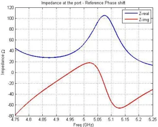
Figure 34: Single antenna port impedance with reference line phase configuration. ... 59
Figure 35: Single antenna port impedance with 90⁰ phase configuration. ... 60
Figure 36: Single antenna port impedance with 180⁰ phase configuration. ... 60
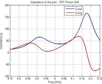
Figure 37: Single antenna port impedance with 270⁰ phase configuration. ... 61
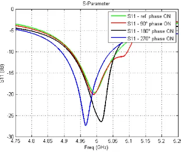
Figure 38: S11 of single antenna with various phase configuration. ... 62
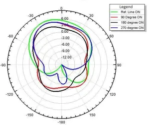
Figure 39: 2D radiation patter - 0⁰ azimuth view ... 63
Figure 40: 2D radiation pattern - 90⁰ azimuth view... 63
Figure 41: Antenna far-field intensity - 0⁰ azimuth view. ... 64
Figure 42: Antenna far-field intensity - 90⁰ azimuth. ... 64
Figure 43: 3D radiation pattern with reference trace ON ... 65
Figure 44: 3D radiation pattern with 90⁰ trace ON ... 65
Figure 45: 3D radiation pattern with 180⁰ trace ON. ... 66
Figure 46: 3D radiation pattern with 270⁰ trace ON. ... 66
Figure 47: Phase shift due to each phase shifter trace plotted using raw data ... 67
Figure 48: Adjusted Phase Shift due to each phase shifter trace ... 68
Figure 49: Change in phase shift due to each additional trace. ... 69
Figure 50: Corporate feed network. ... 70
Figure 51: S11 for the corporate feed network. ... 71
Figure 52: A corporate feed network connected to a phase shifter. ... 72
Figure 53: Antenna Array – top view. ... 73
Figure 54: Antenna Array – side view. ... 73
Figure 55: Antenna excitation with 0⁰, 90⁰, 180⁰, and 270⁰ phase shift to each antenna element. ... 74
Figure 56: S11 of the antenna array feed port with ascending (0⁰, 90⁰, 180⁰, and 270⁰) phase shift. ... 75
Figure 57: Impedance at the feed port for ascending phase shift. ... 75
Figure 58: 2D Radiation Pattern – elevation with ascending phase shift ... 76
Figure 60: Antenna excitation with 270⁰, 180⁰, 90⁰, and 0⁰ phase shift to each antenna
element. ... 77
Figure 61: S11 of the antenna array with descending (270⁰, 180⁰, 90⁰, and 0⁰) phase shift. ... 78
Figure 62: Impedance at the antenna port for descending phase shift. ... 78
Figure 63: 2D Radiation Pattern - elevation with descending phase shift ... 79
Figure 64: 3D Radiation Pattern with descending phase shift ... 79
Figure 65: Antenna excitation with 0⁰ phase shift to each antenna element ... 80
Figure 66: S11 of the antenna array with 0⁰ phase shift. ... 81
Figure 67: Impedance at the antenna port for 0⁰ phase shift. ... 81
Figure 68: 2D Radiation Pattern - elevation with 0⁰ phase shift. ... 82
Figure 69: 3D Radiation Pattern with 0⁰ phase shift ... 82
Figure 70: Combined return loss for different phase configuration ... 83
Figure 71: Combined 2D radiation pattern for three different phase excitations. ... 83
Figure 72: Setup with first antenna element with other ports terminated with 50 Ω. ... 84
Figure 73: Setup with second antenna element with other ports terminated with 50 Ω. .. 84
Figure 74: Setup with third antenna element with other ports terminated with 50 Ω. ... 84
Figure 75: Setup with fourth antenna element with other ports terminated with 50 Ω. ... 84
Figure 76: Impedance with only first antenna ... 85
Figure 77: Impedance with only second antenna ... 85
Figure 78: Impedance with only third antenna ... 85
Figure 79: Impedance with only fourth antenna ... 85
Figure 80: S11 for each isolated antenna. ... 85
Figure 81: Open state of Mercury Wetted switch [13]. ... 87
Figure 82: Closed state of Mercury Wetted switch [13]. ... 87
Figure 83: PE4246 PIN Configuration. ... 88
Figure 84: Switch pads drawn between microstrip lines. ... 89
Figure 85: Control lines and via... 89
Figure 86: Antenna board with Corporate feed network (top side). ... 90
Figure 87: Antenna Board with Control lines (bottom side) ... 90
Figure 88: Antenna as a whole ... 91
Figure 89: Antenna array with control circuit... 92
Figure 90: Fabricated single antenna ... 93
Figure 92: Fabricated single phase shifter on Rogers/Duroid 6006. ... 94
Figure 93: Fabricated single antenna #2 on Rogers/Duroid 6006 ... 95
Figure 94: Fabricated antenna – array side. ... 95
Figure 95: Fabricated antenna – ground plane side. ... 96
Figure 96: Fabricated Phase Shifters – phase shifter side... 96
Figure 97: Fabricated Phase Shifters – Control side. ... 96
Figure 98: A complete antenna – array side. ... 97
Figure 99: A complete antenna – phase shifter side. ... 97
Figure 100: Fabricated antenna – array side (without switches). ... 98
Figure 101: Fabricated Antenna – reference phase shift. ... 98
Figure 102: Fabricated antenna – ascending phase shift. ... 99
Figure 103: Fabricated antenna – descending phase shift. ... 99
Figure 104: Single antenna return loss – reference phase (wrong dielectric). ... 100
Figure 105: Single Antenna return loss - 90⁰ phase (wrong dielectric). ... 101
Figure 106: Single Antenna return loss - 180⁰ phase (wrong dielectric). ... 101
Figure 107: Single Antenna return loss - 270⁰ phase (wrong dielectric). ... 102
Figure 108: Single antenna return loss – reference phase... 102
Figure 109: Single antenna return loss – reference phase... 103
Figure 110: Measured Phase shift due to each phase shifter trace. ... 104
Figure 111: Change in phase shift due to each additional trace ... 104
Figure 112: Measured return loss for 0⁰ beam steering antenna. ... 105
Figure 113: Measured return loss for +45⁰ beam steering antenna... 106
Figure 114: Measured return loss for -45⁰ beam steering antenna. ... 106
Figure 115: Measured and Simulated return loss for broad side beam antenna. ... 107
Figure 116: Measured and Simulated return loss for +45⁰ beam steering antenna... 108
Figure 117: Measured and Simulated return loss for -45⁰ beam steering antenna. ... 108
Figure 118: Measured and Simulated return loss for all three-antenna array. ... 109
Figure 119: Measurement setup inside an anechoic chamber. ... 110
Figure 120: Antenna mount ... 111
Figure 121: Antenna centered with horn antenna. ... 111
Figure 122: 2D radiation pattern for broadside beam antenna. ... 112
Figure 123: 2D radiation pattern for +45⁰ beam antenna... 112
Figure 125: Measured and Simulated 2D radiation pattern – broadside beam. ... 113
Figure 126: Measured and Simulated 2D radiation pattern, 45⁰ beam ... 114
Figure 127: Measured and Simulated 2D radiation pattern, -45⁰ beam ... 114
Figure 128: Measured and Simulated 2D radiation patterns for all three antennae. ... 115
Figure 129: Matlab Simulation with 120⁰ uniform phase shift increments. ... 117
LIST OF TABLES
Table 1: Calculated Antenna Parameters (Single Antenna) ... 38
Table 2: Coaxial cable variables. ... 39
Table 3: Change in antenna dimension after tuning ... 43
Table 4: Change in antenna result. ... 45
Table 5: Change in impedance due to placement of phase shifter network and single stub. ... 51
Table 6: Change in impedance due to placement of second stub. ... 53
Table 7: Change in impedance due to placement of third stub. ... 54
Table 8: Change in impedance due to placement of fourth stub. ... 56
Table 9: Simulation result for single antenna with various phase configuration. ... 59
ABSTRACT
A Miniaturized Phased Array Antenna based on Novel Switch Line Phase
Shifter Module
By
Rudra Timsina
A miniaturized phased array antenna with a uniquely designed switch line phase
shifter to obtain a steerable beam pattern is presented. A 1x4 phased array patch antenna is
designed at 5 GHz using Rogers dielectric material with a relative permittivity of 6.15 and
a thickness of 1.524 mm. Each element of the probe fed PAA are connected to a phase
shifter on a different dielectric substrate. The phase shifter has four equal length microstrip
lines placed in a circular fashion around a via that connects to the antenna at the center.
The addition of each microstrip line is designed to provide a phase shift of 90⁰. This design
provides the ability to place the phase shifter and feed to the antenna in space constrained
locations.
The maximum steering angle obtained was ±45⁰. This design is appropriate for
Wi-Fi applications that requires directional beam pattern, Multiple Input Multiple Output
(MIMO) communications, scanning radars, and other applications requiring steerable
CHAPTER 1: INTRODUCTION
1.1Problem Statement
There are many problems which would benefit from an antenna capable of transmitting
and receiving signals from a desired known direction. Before cable television, the
directional Yagi antennas used had to bemanually adjusted at the right direction to receive
a strong signal. Until 2016, 21 percent of US households depended on antenna reception
for at least one televison in their home [1]. The antenna thus needed to be positioned at
the right direction to maximize received signal strength from a desired broadcast station.
Human exposure to electromagnetic radiation due to cell phone use has shown
effects on human health [2]. The uses of omnidirectional antenna inside a cell phone
transmits the signal with equal strength in all directions. As a result, a part of signal energy
is transmitted to the user’s body as shown in Figure 1.
Figure 1: Cellphone radiation [3].
Other problems which arise include call failure in large crowds due to base station
capacity. Similarly, the onmidirectoinal antennas used in WiFi routers for home use,
trasmit signals with equal strength in all directions. The signal is also transmitted outside
of the house where no one is using the WiFi service thus wasting signal energy. A
directional antenna would reduce this signal spillage, at least from one direction.
A part of these problems exist due to the lack of affordable and compact antenna arrays.
The realization of a compact antenna array capable of transmitting and receiving signals to
and from a desired direction that supports multipath propagation can partially mitigate
many problems.
Phased Array Antennas (PAA) are widely used for various applications requiring fixed
or steerable beam patterns. These antennas provide control over the direction and beam
pattern without mechanically adjusting the antenna position. The beam produced by the
antenna can be steered in a desired angle by changing the excitation phase and amplitude
of individual antenna elements. The PAA provides flexibility to receive a signal from a
direction where the signal path is not obstructed and transmit a signal in any preferred
direction. The applications of the traditional PAA were limited to aerospace and military
use due to high cost, complexity, and the size of the antenna. The use of such antennas is
found mostly in space-based applications [4] and military radars [5]. To obtain a directional
antenna pattern, each antenna element in an array must be fed through a phase shifter. The
realization of a mechanical phase shifter on each antenna element makes an antenna costly
and bulky. Therefore, the implementation of such antennas on a small electronic device is
difficult due to area constraints.
To reduce the size and bulkiness of an antenna, electrical phase shifters are more
are some of the popular electrical phase shifters used in antenna arrays. To reduce the size
of an antenna, a dual band Butler matrix is implemented on a phased array [6]. As the
number of antenna elements increases, the number of such phase shifters must increase,
and as a result, the size of the antenna gets larger. The number of input and output ports in
a Butler matrix is equal. Excitation of each input port provides a specific directional beam
pattern of an antenna. The direction of an antenna beam can be controlled using this
method; however, the phase shift on each antenna element cannot be controlled
independently. Therefore, a broadside beam cannot be obtained using this method. A Butler
matrix can be formed with 4, 8 or 16 input/output ports. Hence, an antenna array with a
different number of antenna elements cannot be realized. The Butler matrix must be
stacked up if it is used to feed a planar array, thus increasing space and complexity of the
design.
1.2Objectives
The research advancement in patch antenna and microstrip-based phase shifters makes
it possible to realize antenna arrays for a wide range of applications. Today, antenna arrays
are employed on Wi-Fi, LTE technology [7], and health care applications [8]. In this
project, we design a phase shifter for a four-element linear patch antenna array. The antenna
is designed at 5 GHz; however, the concept of the phase shifter can be applicable for
diverse applications in other frequency bands. Our goal is to design a phase shifter small
enough to fit within the antenna element spacing so that its realization is possible under
each antenna unit.
In a switch-line phase shifter, the input signal is routed through different length
is obtained using a switch-line phase shifter as in [9] and [10]. A four-bit switch-line phase
shifter is realized in [9] using Micro-electro-mechanical switches (MEMS) where different
length transmission lines are switched to obtain desired phase shifts. In [10], a constant
phase shift is produced by switching a reference transmission line with a phase shifting
line. In current designs, the length of the transmission lines switched to obtain phase shifts
are longer and do not fit within antenna element spacing. In our proposed design, the phase
shift is provided by extending a transmission line using RF switches along a circular path
around the via that feeds the antenna. If the circular traces are branched at four equal
lengths to feed the coaxial fed antenna at the center, four phases of 0⁰, 90⁰, 180⁰, and 270⁰
is expected to be achieved. The uses of the Butler matrix in modern wireless
communications [11] and 5G technologies [12] can be substituted with the proposed design
to reduce the overall antenna array dimensions.
The initial goal of this project was to find an application for US patent US5912606A
[13] granted to UNH. This is a patent owned by Northrop Grumman and granted to UNH
for application development. The usefulness of this patent will be discussed later in design
section.
1.3Organization of the Thesis
The chapters of this thesis are organized as follows:
• Chapter 2 provides background information necessary to carry out this project. This
chapter explains theory on transmission lines, microstrip antennas, phased array
antennas and provides a brief explanation of antenna terminology used throughout
• Chapter 3 explains in detail on how the antenna is designed. This chapter also
describes the steps carried out in High Frequency Structural Simulator (HFSS) to
perform antenna simulation. The simulation results are also presented in this
chapter.
• Chapter 4 shows how the antennae are fabricated. This chapter presents pictures of
all fabricated antennae.
• Chapter 5 presents a comparison of both anechoic chamber tests and simulated
radiation pattern results for the antenna.
CHAPTER 2: BACKGROUND
This chapter contains the background material necessary to interpret the work
presented in this thesis. The concepts of antenna theory that supported the realization of a
phased array antenna are explained in brief.
2.1 Antenna Terminology
The antenna terminology explained below will be used throughout the
thesis. Each of the terms are briefly explained below.
2.1.1 Radiation Pattern
The radiation pattern depicts the power emitted by an antenna as a function of
spatial coordinates. The power emitted in the far-field region is usually considered to
determine the radiation pattern of an antenna. The radiation pattern is called a field pattern,
if an electric or a magnetic field is visualized on a spatial coordinate system. If the
distribution of power density is represented as a radiation pattern, it is called the power
pattern [14]. The electric and magnetic field are perpendicular to each other in the far field,
and hence, they produce the elevation and azimuth in a radiation pattern for a horizontally
polarized antenna. The field parallel to the antenna plane is called azimuth and the field
normal to the antenna is called elevation.
Radiation patterns are used to visualize the antenna’s response to an input radio
frequency signal. To better visualize the response of the antenna, a radiation pattern is
usually normalized by its maximum value. The normalized field pattern is obtained by
field pattern is dimensionless. The equation of normalized field pattern is shown in equation (1). max ) , ( ) , ( ) , ( E E
E n = (1)
On a spherical coordinate system, if we assume the main lobe has its maximum in
z direction (θ= 0), the θ component of an electric field is given byE(,) [15].
Power patterns are expressed in terms of Poynting vectorS(,). The normalized
power pattern is obtained by diving the Poynting vector by its maximum value. Equation
(2) shows the normalized power pattern. Both field patterns and power patterns can also be
expressed in the decibel units relative to field maximum value. [15]
max ) , ( ) , ( ) , ( S S
Pn = (2)
The Figure 2 shows a radiation pattern of a patch antenna placed on xy plane. A
radiation pattern of a directional antenna has a narrow width and is pointed to a desired
direction with a dominant main lobe.
2.1.2 Radiation Intensity
The Radiation Intensity is defined as the power radiated from an antenna per unit
solid angle. The unit of radiation intensity is watts per steradian [15]. Steradian is the angle
at the center of a sphere subtended by a spherical surface area equal to one radius square.
The radiation intensity is measured in the far-field region of the antenna.
2.1.3 Beamwidth
Beamwidth is the angular width of an antenna radiation pattern. The width is
measured on a principal lobe of a radiation pattern. To measure the beam width, two
identical points are taken on opposite sides of the main lobe. Beamwidth can be measured
at any points on a radiation pattern, but most commonly used beamwidths are measured at
the half power level and null points. Half Power Beamwidth (HPBW) is measured where
the power level is half (-3 dB) the maximum power represented by a radiation pattern.
Similarly, First-Null Beamwidth (FNBW) is measured between first nulls of the principal
radiation pattern. The Figure 3 illustrates the measurement of HPBW and FNBW.
2.1.4 Directivity
The directivity of an antenna is the ratio of the radiation intensity to the average
radiation intensity of an antenna. The directivity can also be defined as the ratio of
maximum to average Poynting vector [15]. A higher value of directivity implies a relatively
stronger main lobe and very few minor lobes. Greater directivity is obtained if the solid
angle of the main-lobe is small. The unit of directivity is dimensionless. The equation (3)
shows the ratio of directivity.
average
average S
S U
U
D= (,)max = (,)max (3)
Where, D is the directivity,U(,)max is the maximum radiation intensity and Uaverage is
the average radiation intensity. S denotes the Poynting vector.
2.1.5 Antenna Gain
Antenna performance is also measured in terms of gain. The gain of the antenna is
defined as the ratio of intensity measured in a given direction to that of an isotropic antenna.
A conceptual isotropic antenna radiates energy uniformly in all directions. Isotropic
antennas are a useful abstraction, but it is used as a reference “antenna” to compare real
antenna gain. The radiation intensity of an isotropic antenna is equal to the input power to
the antenna divided by 4π steradians[14]. Thus, the equation for antenna gain is shown in
equation (4).
in
P U
The gain of an antenna is usually measured in dBi or dBd. When the gain is
measured in reference to an isotropic radiator, the unit of dBi is used. When the gain is
measured in reference to a dipole antenna, the unit of dBd is used.
2.1.6 Antenna Efficiency
Antenna efficiency is the ratio of the power radiated from the antenna to the input
power of the antenna. The isotropic antenna is the ideal antenna and has efficiency of 1.
Efficiency of 1 cannot be obtained practically. The efficiency of the antenna is affected by
the conduction and dielectric losses. A part of energy received or transmitted by an antenna
is converted into heat. Same energy is lost due to finite conductivity of the material used
in the antenna. The equation (5) shows the formula to obtain efficiency of the antenna.
in radiated
P P
Efficiency= (5)
2.1.7 Bandwidth
The bandwidth of an antenna is the range of frequencies over which the antenna
performance is acceptable. The bandwidth is taken as the range of frequencies around the
design center frequency over which acceptable performance is obtained. The range is
chosen based on the application the antenna is designed for. The bandwidth can be
measured using antenna parameters like Voltage Standing Wave Ratio (VSWR), return
loss, antenna gain or antenna impedance. These antenna parameters vary over the range of
frequencies. The desired frequency range is the bandwidth where the chosen antenna
2.1.8 Polarization
The polarization of an antenna is defined as the orientation of the transmitted
electric field in the far field region. The time-varying electric field vector traces a locus in
a direction that determines the antenna polarization. Therefore, polarization provides the
direction of propagation of instantaneous electric field for transverse waveforms. The most
common types of wave polarization are, linear, circular, and elliptical. If the vector that
represents the electric field propagates along a line in space, the wave is considered to be
linearly polarized. Elliptical polarization occurs when the curve traced by the vector
electric field is elliptical. Similarly, the circular trace of the vector field produces circular
wave polarization. Linear polarization and circular polarization are special cases of
elliptical polarization. The elliptical path of the vector field changes to become a line or a
circle and produce linear and circular polarization respectively [14]. The circular or
elliptical polarized wave can either traces a curve in clockwise or a counter-clockwise
direction. The curve with clockwise instantaneous fields is right-handed. The curve with
counter-clockwise instantaneous fields are left-handed [14]. The circularly polarized wave
field is shown in Figure 4.
2.2 Transmission Line
When dealing with high frequency design, transmission line theory must be
incorporated. At DC, the voltage along the transmission line remains considerably uniform.
The same case does not apply with radio frequency signals. As the frequency increases, the
wavelength of the signal decreases. At high frequency, the wavelength of the signal can be
comparable to the size of the electronic components used. When the components used are
of few wavelengths long, it causes a variation of voltage along the transmission line [17].
Voltage variation is caused due to loss in the transmission line. The loss is introduced due
to resistance, capacitance and inductance on the line. A microstrip trace on a dielectric
substrate must be carefully designed to minimize the losses to ensure maximum power
transfer. The topics associated with transmission lines are discussed below. The formulae
that follow are very useful to carry out the design.
2.2.1 Transmission Line Types
There are two types of transmission lines incorporated in this project. Each types
are described below.
2.2.1.1 Coaxial Line
Coaxial cables are widely used in many RF applications. This cable is designed to
minimize the interference and radiation loss. Coaxial cables are made with an inner
conductor, dielectric layer, and outer conductor. The dielectric layer lies between the inner
conductor and outer conductor. For maximum power transfer, the cable characteristic
antenna designed in this project is for 50 Ω applications. The formula shown in equation
(6) and (7) determines the characteristic impedance of a coaxial cable [18].
= b a Z ln 2 1 0 (6) b a Z r 10 0 log 138 (7)
Where, = Permeability of dielectric medium
= Permittivity of dielectric medium.
r= relative permittivitya = Inner radius of the outer conductor of coaxial cable.
b = Radius of the inner conductor of coaxial cable
2.2.1.2 Microstrip Line
Microstrip lines are conducting traces on a dielectric substrate. The other side of
the substrate has a ground plane. The dimension of the conducting traces must be carefully
determined to obtain an optimal result. At higher frequencies, microstrip lines suffers
radiation, conduction, and dielectric losses [17]. To ensure maximum power transfer, the
impedance of the transmission line must be matched to the RF circuit.
Due to the presence of a dielectric substrate, the microstrip line suffers from
fringing effects at the edge of the patch [14]. Figure 5 shows the electric field lines on a
microstrip transmission line. Due to the presence of two dielectrics, air and the substrate,
the field lines look nonhomogeneous. Most of the electric field lines reside inside the
line to the height of the dielectric substrate is much greater than 1 and the relative
permittivity of the substrate is much greater than 1, the field lines mostly remains inside
the substrate. Due to the presence of some field lines in the air, the width of the transmission
line looks electrically wider than its actual width. To account for the fringing effect, an
effective dielectric constant is introduced [14].
Figure 5: Microstrip transmission line and the electric field lines [14].
The effective dielectric constant when w/h <1, is calculated using equation
(8) [17].
− + + − + + =
−1/2 2
1 04 . 0 12 1 2 1 2 1 h w w h r r eff (8)
Where, h = height of the dielectric substrate
w = width of the transmission line
Thus, the impedance of the transmission line is given by equation (9).
Where Zf = wave impedance in free space (377 ohms)
Similarly, for a transmission line having w/h > 1, the effective dielectric constant is given
by equation (10).
+ − + + =
−1/2
12 1 2 1 2 1 w h r r eff (10)
The characteristic impedance of the line is then given by equation (11).
+ + + = 444 . 1 ln 3 2 393 . 1 0 h w h w Z Z eff f (11)
2.2.2 Voltage Reflection Coefficient (Γ)
The voltage reflection coefficient is an important parameter when designing
microstrip transmission lines. It is measured when the transmission line is terminated with
a load impedance. The reflection coefficient is measured in terms of the characteristic
impedance of the transmission line and the load impedance. The equation (12) below is
used to calculate the reflection coefficient [17].
0 0 0 Z Z Z Z L L + − = (12)
Where, ZL= load impedance of the transmission line
Z0= characteristic impedance of the transmission line
When the transmission line is open, the load impedance is infinity and hence the reflection
coefficient is 1. The reflected wave has the same polarity as the input wave. When the line
is shorted, the load impedance is 0, and therefore the reflection coefficient is -1. The input
To obtain maximum power transfer, the impedance of the load must match the
characteristic impedance.
2.2.3 Voltage Standing Wave Ratio (VSWR)
Reflection in the transmission line is caused by an impedance mismatch in the line.
The VSWR shows the amount of mismatch in the transmission line. The value of VSWR
ranges from 1 to infinity. If there is minimum reflection on a transmission line, the value
of VSWR tends to be near 1. A complete reflection of a signal in a transmission line has
value of VSWR reaching infinity. Mismatch is measured in terms of amplitude of the
signal. The ratio of the maximum voltage to the minimum voltage along the line determines
the VSWR [17]. It is also represented in terms of reflection coefficient. Equation (13)
shows VSWR as a function of reflection coefficient.
0 0 1 1 − + = VSWR (13)
2.2.4 Input Impedance
Input impedance allows us to determine how the load impedance is transferred
along a transmission line. The input impedance of a lossless transmission line with
characteristic impedance of Z0 at a distance d away from the load ZL, is given by equation
(14) [17]. ) tan( ) tan( ) ( 0 0 0 d jZ Z d jZ Z Z d Z L L in + + = (14)
Where, d = distance away from load
β = wave number given by
2
2.2.5 Return Loss and Insertion Loss
Return loss measures the amount of signal returned in the transmission line due to
a fault in the line. The fault can be an impedance mismatch in the line or the load. The
return loss is the ratio of reflected power to the incident power [17]. The equation for return
loss is shown in equation (15). It can be measured in terms of reflection coefficient.
in i r P P dB
RL =−
−
= 10log 20log ]
[
(15)
Where, Pr = reflected power
Pi = incident power
Γin = Reflection coefficient at the input of the transmission line.
Similarly, the insertion loss is a ratio of transmitted power to the incident power. The
equation for insertion loss is shown in equation (16).
(
2)
1 log 10 log 10 ] [ in i t P P dB
IL =− −
− = (16)
Where, Pt=transmitted power.
2.2.6 Impedance Matching
To solve the problem of reflection on the transmission line of an antenna, the
impedance can be matched so that maximum power is transferred. There are two kinds of
matching techniques used in this project. These methods are explained below.
2.2.6.1 Quarter Wave Transformer
A quarter wave transformer is a transmission line which is an electrical quarter
line, a desired input impedance can be achieved to match with the load impedance [17]. If
the distance d in equation (14) is substituted with quarter wavelength, i.e. 4
, the
characteristic impedance of the quarter wave transformer is obtained.
+ + = = 4 2 tan 4 2 tan ) 4 ( 0 0 0 L L in jZ Z jZ Z Z d Z (17) Since,
= 2
Therefore,
in LZ
Z
Z0 = (18)
2.2.6.2 Stub Matching
Using discrete components to transform the impedance in a transmission line for
high frequency applications is challenging due to the size of the components. The matching
is also achieved using open or shorted microstrip traces in a transmission line. Every
conducting trace on a dielectric substrate possess some resistance, inductance and
capacitance. To cancel out the capacitance or inductance in a transmission line, a stub is
added to the line. The characteristic impedance of the stub is often the characteristic
impedance of the transmission line. The impedance is made equal so that the input
impedance seen by the source does not vary with load impedance. The parallel combination
of the input impedance of the line and the stub are made equal to the characteristic
impedance at the stub location. The mathematics involves a set of non-linear equations
the position of the stub from the load [19]. The position of the stub is valid for both open
and shorted stubs.
+ − − = − 2 2 1 ) 1 ( 1 tan 1 L L L L L b g g b g d (19)Where, gL = conductance, real part of admittance
bL = susceptance, imaginary part of admittance
The length for the open stub is given by equations (20) and (21).
+ − = − 2 2 1 ) 1 ( tan 1 L L L stub b g g L (20) + − − = − 2 2 1 ) 1 ( tan 1 L L L stub b g g L (21)
Similarly, the length of the shorted stubs is given by equations (22) and (23) .
− + − = − L L L stub g b g L 2 2
1 (1 )
tan 1
(22)
− + = − L L L stub g b g L 2 2
1 (1 )
tan 1
(23)
2.2.7 Scattering Parameters (s-Parameters)
The scattering parameters describe the input-output relationship of waves passing
through a multiport network. Not all the signal that passes through the input terminal of a
system gets through to the output terminal. Some of the energy is reflected due to
a measure of the signal at the system’s port in terms of incident and reflected power [17].
Scattering parameters are denoted by Sij, which gives the response at port i due to an
incident signal at port j. For a two-port network shown in Figure 6 , four parameters – S11,
S21, S12 and S22, can be computed or measured.
Figure 6: S-parameters in a two-port network.
The S-parameters in a matrix form are shown in equation (24) [17].
= 2 1 22 21 12 11 2 1 a a S S S S b b (24) Where 1 port at power incident 1 port at power reflected 0 1 1 11 2 = = = a a b S (25) 1 port at power incident 2 port at power d transmitte 0 1 2 21 2 = = = a a b S (26) 2 port at power incident 2 port at power reflected 0 2 2 22 1 = = = a a b S (27) 2 port at power incident 1 port at power d transmitte 0 2 1 12 1 = = = a a b S (28)
S-Parameters provide many useful measurements in RF circuits. S11 is a reflection
coefficient at the input terminal of the system. The return loss is measured in terms of S11.
magnitude of the input reflection coefficient. The insertion loss is measured in terms of S21.
It is obtained by taking the logarithm of the magnitude of S21 [17]. Similarly, S22 is the
reflection coefficient at the output port. The return loss at the output port can be obtained
using this parameter. Insertion loss at the output port can be computed using S12.
2.2.8 Impedance Parameters (Z-parameters)
Similar to the s-parameters, impedance parameters or z-parameters provide the
input-output impedance relationship in a two-port network. The impedance parameters can
also be expressed in terms of reflection coefficients. Impedance parameters are obtained
by keeping the input or output terminals of the system open circuited. Hence, the
z-parameters are also called open-circuit impedance parameter. The z-parameter matrix for
a two-port network is shown in equation (29).
= 22 21 12 11 Z Z Z Z Z (29)Where, Z11 = Open circuit input impedance
Z12 = Open circuit transfer impedance from port 1 to port 2
Z21 = Open Circuit transfer impedance from port 2 to port 1
Z22 = Open circuit output impedance
2.3 Microstrip Antenna
A microstrip antenna consist of a metallic patch on a dielectric substrate. The other
side of the dielectric substrate may contain a ground plane. The antenna is excited through
substrate thickness and other antenna parameters are chosen to obtain maximum radiation
at the desired frequency. Microstrip patch antennas are very appropriate for electronics that
have size and weight constraints and that require low cost antennas. The size of the antenna
reduces as the frequency increases; therefore, patch antennae are very suitable for high
frequency applications. This antenna can be manufactured inexpensively using printed
circuit board technology [14]. For low frequencies, the size of the antenna is too big to be
fabricated on a circuit board. Patch antennas can be easily designed and developed for any
shape and size based on the system requirements. There are also some disadvantages of
using patch antennas. Patch antennas are not suitable for wide-band applications. This
antenna has low efficiency, operates at low power and has poor scan performance [14].
The desired polarization, radiation pattern, resonant frequency and impedance can be easily
achieved by altering the antenna parameters. For instance, a thicker dielectric can be used
to obtain wide bandwidth [14].
2.3.1 Rectangular Patch Antenna
The size of the antenna for this project is obtained by using transmission line model
analysis. Similar to the microstrip line, a patch antenna also suffers fringing effect. As
shown in Figure 5, the electric field lines are nonhomogeneous due to the presence of air
and dielectric substrates near the patch. To account for the fringing effect, an effective
dielectric constant must be determined using
(8) and (10). The length of the antenna must be extended by a small length to
calculated by using the effective dielectric constant. Equation (30) is used to obtain the
extension length ∆L [14].
(
)
(
)
+ − + + = 8 . 0 258 . 0 264 . 0 3 . 0 412 . 0 h W h W h L eff eff (30)Where, W = width of the antenna
Each side of the patch antenna is extended by length ∆L. Thus, the effective length of the
antenna is given by equation (31) [14].
L L
Leff = +2 (31)
Where L = Nominal design length of the antenna
The effective length of an antenna is a factor of the effective dielectric constant and the
resonance frequency. Thus, the effective length is calculated using equation (32) [14].
0 0 2 1 eff r eff f
L = (32)
Where 𝑓𝑟 = resonance frequency
𝜇0 = permeability of free space (4π x 10-7 N/A2)
𝜀0 = permittivity of free space (8.854x10⁻¹² F/m)
The equation to calculate the actual length of an antenna is obtained by substituting
equation (32) in equation (31). Therefore, equation (33) gives the actual length of an
The width of an antenna is a function of dielectric constant and the resonant frequency.
The width is calculated using equation (34) [14].
1 2 2 1 0 0 + = r r f W (34)
An antenna provides maximum radiation if the input impedance of the antenna is matched
with the feed line. Typical values of impedance at the edge of a rectangular patch antenna
ranges from 100 to 400 Ω [20]. For an edge fed antenna, the input impedance is given by
(35) [20]. − = 2 2 1 90 W L Z r r (35)
The input impedance is a function of dielectric constant, length and width of the antenna.
The impedance value can be reduced by increasing the width of the antenna. However, the
ratio of the width to the length of the antenna must remain below 2, to keep the aperture
efficiency of the antenna at a reasonable level. As the ratio increases over 2, the efficiency
starts dropping [14]. The impedance can also be adjusted by choosing appropriate feeding
methods and feed locations.
2.3.2 Feeding Methods
There are many ways to feed a microstrip patch antenna. Feeding methods are
classified into three different kinds; directly coupled, electromagnetically coupled and
aperture coupled [20]. Different techniques are applied to each feeding method to obtain
the desired input impedance at the antenna port. Figure 7 shows the various kinds of
The edge feed and the coaxial feed are different kinds of direct feed. Edge feed are
directly attached to the edge of the patch antenna. The feed line is printed on the same layer
as the antenna. Edge feed can be realized either with a quarter wave transformer or an inset.
The input impedance of the antenna can be matched to the feed line with a quarter
wavelength long transmission line. The characteristic impedance of the quarter wavelength
transmission line is determined using equation (18).
For an inset fed antenna, the feedline distance into the antenna is adjusted to achieve
the needed impedance. For a high permittivity substrate, the inset depth may be not
practical to realize as it affects cross polarization and radiation pattern [20]. The inset feed
scales the input impedance in (35) as shown in
(36) [20].
(
0)
cos )
( 2 =
=
i i
i Z x
L x x
Z
(36)
Where, ∆xi = inset depth from the edge of the antenna.
In this project, the antenna is fed by a combination of coaxial feed and a corporate
feed. The idea of quarter wave transformer is used to realize the corporate feed network.
Figure 7: Different feeding techniques on a patch antenna [20].
The coaxial feed is another kind of direct coupled feed method. The inner conductor
of the coaxial cable is probed through the dielectric substrate and is connected with the
antenna patch. The outer conductor of the coaxial cable is connected to the ground on the
other side of the dielectric substrate. The impedance is adjusted by changing the feed
location. The distance between the edge of the antenna and the feed location is changed to
obtain the desired impedance. As the distance from the edge of the antenna is increased,
the impedance in equation (35) is scaled as shown in
(37) [20].
(
0)
cos )
( 2 =
=
p p
p Z x
L x x
Z (37)
The coaxial feed and the edge feed can also be implemented by keeping a small gap
between the feedline and the antenna. These are the types of electromagnetically coupled
feeding method is sometime advantageous over the probe feed. The gap between the
feedline and the antenna will introduce some capacitance. The reactance part of the
impedance is minimized, as the capacitance introduced from the gap cancels out the probe
inductance [20].
In an aperture feed, two different dielectric substrates are used for an antenna and
the feed line. The two substrates are separated by a ground plane. The feedline lies at the
bottom of the lower dielectric substrate. The signal from the feed line is coupled with the
antenna through a slot on a ground plane separating two substrates. The upper substrate is
typically thicker and has low dielectric constant. The lower substrate has higher dielectric
constant [14]. The thicker dielectric is very useful for wide-band applications. The antenna
also possesses less spurious radiation since the ground plane between the substrate partially
isolates the feed from the radiating element.
2.4 Phased Array Antenna
A single antenna is limited to a fixed gain and directivity. A single antenna element
produces a wide radiation pattern, and the direction of the radiation beam cannot be
controlled. A communication system, that requires high directivity and gain requires a
directional antenna. One way to achieve high directivity is to use multiple antenna
elements. Antenna elements can be arranged in a linear or planar geometry to form an
array. In a phased array antenna, the amplitude and phase of the signal that feeds the
antenna elements can be controlled to obtain a radiation pattern in a desired direction. The
electric field strength of an antenna array is the sum of the electric fields of the individual
antenna elements. The distance between the antenna elements, the phase and amplitude
radiation pattern [14]. Phased array antennas are widely used for applications that require
fixed or steerable beam patterns. These antennae provide control over the direction and
beam pattern without mechanically adjusting the antenna position. The phased array
antenna provides flexibility to receive signals from a direction where the signal path is
obstructed and transmit signals in any desired direction.
In this project a four-element linear array of patch antennas is designed and
realized. The distance between each antenna element is uniform. The derivation of the
electric field that contributes to shape the radiation pattern is shown below.
Let us assume the separation between the antenna elements is d. As shown in Figure 8, x
is a distance of delay between adjacent antennas. R is the far-field distance of the antenna.
The delay distance can be calculated as shown in equation (38).
cos
d
x= (38)
Where θ = direction of the main beam
Now let us calculate a small phase change due to antenna separation. The ratio of delay
distance to the wavelength is proportional to the ratio of phase change over 360o.
x = 2 (39) x x = =
2 (40)
Substituting x in equation (40) from (38), the change in phase due to antenna element
separation is obtained as shown below in equation (41).
= dcos
(41)
To obtain beam steering, the signal going to each antenna element will have some phase
excitation. In this calculation, the phase change on consecutive antenna element are
assumed to be uniform. If the input current to the first antenna element is Io, then the input
current to other antenna element is given by equations below.
0 1 I
I = (42)
j
e I
I2 = 0 (43)
2 0 3 j e I
I = (44)
( 1)
0
−
= jN
N I e
I (45)
Where = input current phase shift.
Now, the electric field on each antenna element can be calculated using the input current
to the antenna. The electric field on the first antenna element is given by equation
(46). The mutual coupling between antenna elements is not considered while developing
0 0
1
4 R E e I E R j = = − (46)
The electric field for second and third element can be calculated as shown below.
) cos ( 0 0 2 4 + + − =
= j d
j R j j e E R e e I E (47) ) cos ( 2 0 2 2 0 3 4 + + − =
= j d
j R j j e E R e e I E (48)
Similarly, the far electric field for Nth antenna element is given by equation (49).
) cos )( 1 ( 0 ) 1 ( ) 1 ( 0 4 + − − + − − =
= jN d
N j R j N j
N E e
R e e
I
E (49)
The radiation energy in the far field of the antenna is the sum of energy radiated through
the individual antenna elements. Therefore, the total electric field of an antenna array
spaced in a uniform geometry and excited with uniform phase shift is given by equation
(50). ) cos )( 1 ( 0 ) cos ( 2 0 ) cos ( 0 0 .... + + + + + − + +
= j d j d j N d
e E e E e E E E (50)
( cos ) 2( cos ) ( 1)( cos )
01 ....
+ + + + + − + +
= j d j d j N d
e e e E E AF E
E= 0 (51)
Where, AF = Array Factor
Therefore, the total electric field of an antenna array is the product of the electric field of a
single antenna element and the array factor. The mutual coupling between the antenna
elements is not accounted for in the equation. The array factor is the function of the antenna
spacing, input signal phase, and the wavelength. These parameters are key in determining
the antenna radiation pattern. Thus, the directivity of the antenna is shaped by the array
) cos )( 1 ( ) cos ( 2 ) cos ( ....
1+ + + + + + − +
= j d j d j N d
e e e AF (52)
= + − = n N d N j e AF 1 ) cos )( 1 ( (53)Where, n = number of antenna element in an array
Let, =dcos + (54)
Therefore,
= − = n N N j e AF 1 ) 1( (55)
The equation (55) is the simplified array factor equation for a linear phased array antenna.
2.5 High Frequency Structural Simulator (HFSS) Background
The phased array antenna was designed using a three-dimensional electro-magnetic
simulation tool called High Frequency Structural Simulator (HFSS). HFSS uses a
computational technique called Finite Element Method (FEM) to solve for fields in an
antenna structure. A mesh network is formed by dividing the antenna geometry into many
small tetrahedron shapes to apply FEM analysis. The electric field for each tetrahedron
geometry is solved by applying a boundary condition. The boundary condition is applied
between the adjacent shapes. The vector field is calculated at each edge of the mesh
element. The field vector is then interpolated within the element geometry to calculate the
total field. Thus, the accuracy of the total field depends on the number of tetrahedrons in a
mesh. Increasing the number of tetrahedron shapes in a mesh will decreases the size of
each mesh element. The accuracy of the result increases with smaller tetrahedron size but
Figure 9 : Mesh network of a tetrahedron geometry on a probe fed patch antenna.
HFSS performs adaptive iterative solution to compute an accurate result. To perform
iterative solution, the size of the mesh network is refined iteratively until an optimal
solution is found. The vector field solution is used to calculate the scattering matrix. The
amount of transmission and reflection that occurs inside the antenna geometry determines
the scattering parameters [22]. Figure 9 shows the mesh network of tetrahedron geometry
on a probe fed patch antenna.
There are some conditions in HFSS that need to be established to solve an antenna
structure. The software must know the antenna material, boundary condition, solution
model, and excitation to perform an electromagnetic analysis. Some of the HFSS
2.5.1 Antenna Geometry
A two or three-dimensional structure of any shape and size can be formed in HFSS.
The size of the antenna is determined using the equations provided in previous sections of
this thesis. Complex shapes can be formed by subtracting and uniting various components
together or drawing equation-based surfaces. The software also allows to import drawings
from other design tools. The geometrical shapes must be assigned a material for the
software to accurately compute the associated field.
2.5.2 Boundary Conditions
The boundary condition can be applied to a two-dimensional object or a surface of
a three-dimensional object. Some of the boundary conditions applied in this project are:
finite conductivity, lumped RLC, Radiation boundary, and Perfectly Matched Layer (PML)
boundary. The boundaries are used in HFSS to simplify the solution. A boundary can create
an open or closed model. A boundary for a closed model will not let energy radiate out of
the boundary. The boundary condition also simplifies the geometric complexity [22]. For
instance, a boundary condition applied to a geometry can replace a lumped parameter such
as resistor, inductor or a capacitor.
A finite conductive boundary or a boundary with Perfect Electric Conductor (PEC)
can be established on a two-dimensional object like patch antennas or microstrip traces.
The PEC boundary represents a lossless conductor and is applied to traces with an infinite
ground plane. The finite conductivity represents an imperfect conductor and is applied to
The lumped RLC boundary is an impedance boundary that is used to replace
lumped components. The RLC boundary uses resistor, capacitor, and an inductor in
parallel. To obtain a series combination of the lumped component, two different geometries
must be placed in series and assigned a lumped RLC boundary. The RLC values assigned
to the boundary provide ideal behavior of the components [22].
The radiation boundary creates a space for radiating objects like an antenna to
radiate waves into infinite space. This boundary is placed one-quarter wavelength away
from the antenna. Each surface of a radiation box is assigned a boundary so that the wave
does not propagate outside the box. The wave is absorbed at the radiating boundary [22].
Similar to the radiation boundary is a PML boundary. This boundary is also applied outside
the radiating surface. The wave reaching the radiation boundary is absorbed perfectly if the
wave is incident normal to the radiating surface. For a phased array antenna, the radiated
energy is steered at different angles. The wave is not absorbed as desired if the wave is
incident at an angle. Therefore, the PML boundaries are used while simulating antenna
structures that produces radiation pattern at an angle. Figure 10 shows the absorption of a
Figure 10: Wave absorption at the radiation boundary at different angle of incidence
A PML boundary has an additional layer of anisotropic material that absorbs the
electromagnetic field reaching the surface.
Figure 11 shows a PML boundary.
2.5.3 Excitation
Antennas are excited with a source of current, voltage, or field at the antenna port.
The most common excitation types in HFSS are the wave port and the lumped port. These
excitations provide field behavior of the antenna. An impedance parameter, scattering
parameter, and admittance parameter can be requested if these ports are used in the
simulation. Antennas are excited using a wave port at the outer surface of the solution
space. This port is located at the radiation boundary. The lumped port is used when it is not
relevant to use a wave port. If an antenna must be excited from within the dielectric
substrate, the use of wave port is not applicable. A lumped port can be used inside the
radiation boundary and within the dielectric material. In both excitation types, an
integration line must be drawn from ground to the feed line.
2.5.4 Post Processing
The behavior of an antenna can be interpreted using results in HFSS after successful
completion of the simulation. Some of the results that are useful in determining the antenna
performance are the scattering parameter S11, impedance parameter, 2D and 3D radiation
patterns, and VSWR. The calculated dimension of an antenna does not always guarantee a
desired performance. Therefore, antenna dimensions must be tuned so that the desired
performance of an antenna can be achieved. During solution setup, derivatives can be
requested on variables responsible to affect the solution. When a derivative on a variable
is requested, HFSS solves for the field when there is 10% change in dimension. After the
Parametric analysis is another option in HFSS. A range of values can be assigned
to a variable and HFSS will provide result for every value. The assigned values can be in
linear step, linear count, decade count, octave count, and exponential count. The correct
dimension of the antenna parameter that yields the desired result can be assigned to the
![Figure 3: 2D Radiation pattern showing half power beamwidth and first-null beamwidth [14]](https://thumb-us.123doks.com/thumbv2/123dok_us/9655638.1493375/21.612.248.403.486.660/figure-radiation-pattern-showing-half-power-beamwidth-beamwidth.webp)