N A N O E X P R E S S
Open Access
Chemical characterization of extra layers at the
interfaces in MOCVD InGaP/GaAs junctions by
electron beam methods
Cesare Frigeri
1*, Alexey Aleksandrovich Shakhmin
2, Dmitry Anatolievich Vinokurov
2,
Maria Vladimirovna Zamoryanskaya
2Abstract
Electron beam methods, such as cathodoluminescence (CL) that is based on an electron-probe microanalyser, and (200) dark field and high angle annular dark field (HAADF) in a scanning transmission electron microscope, are used to study the deterioration of interfaces in InGaP/GaAs system with the GaAs QW on top of InGaP. A CL emission peak different from that of the QW was detected. By using HAADF, it is found that the GaAs QW does not exist any longer, being replaced by extra interlayer(s) that are different from GaAs and InGaP because of atomic rearrangements at the interface. The nature and composition of the interlayer(s) are determined by HAADF. Such changes of the nominal GaAs QW can account for the emission observed by CL.
Introduction
Several devices, such as HBTs, HEMTs, solar cells and LEDs, are currently based on InGaP/GaAs heterojunc-tion because of its superior properties with respect to AlGaAs [1-4]. The InGaP/GaAs system, especially if it is grown by metal organic vapour phase deposition (MOCVD), has, however, the drawback that the inter-faces between InGaP and GaAs are deteriorated, as shown by photoluminescence, X-ray diffraction and transmission electron microscopy (TEM), because there is no common group V element across the interface [5]. This mostly affects the inverted GaAs-on-InGaP inter-face where an unwanted extra interlayer forms, which recombines the minority carriers more efficiently than the GaAs quantum well [5-10]. The normal InGaP-on-GaAs interface is always good, but this is not sufficient to guarantee reliable device performance. The deteriora-tion of the inverted GaAs-on-InGaP interface has been seen to occur in practically every MOCVD InGaP/GaAs heterostructure containing such an interface, to a more or less great extent depending on the growth conditions [5-10]. It could sometimes be avoided by the use of growth interruption between the layers [6], the growth
on top of InGaP of a thin (1 nm) intentional interfacial layer of GaP [5,7,9] or GaAlAs [8], or the application of a preflow of trimethylgallium on the InGaP surface before switching on the AsH3flow [11].
A recent contribution to this field was based on catho-doluminescence (CL) measurements [12,13]. The differ-ence between the two interfaces was confirmed by comparing two InGaP/GaAs systems containing a GaAs QW and either one of the two interfaces [12,13]. One sample had the layer sequence GaAs substrate/GaAs buffer/AlGaAs/GaAs/InGaP with the normal interface. It showed the expected GaAs QW emission (1.56 eV at 77 K). The other sample had the sequence GaAs sub-strate/GaAs buffer/InGaP/GaAs/AlGaAs with the inverted GaAs-on-InGaP interface. This sample did not exhibit the expected QW emission. On the contrary, a CL peak was seen at 1.48 eV, which suggested that the GaAs QW was absent, having been replaced by a transi-tion layer of InGaAsP with mixed compositransi-tion [12,13]. The aim of this study is to check by TEM whether the CL results can be related to structural modifications of the GaAs QW, such as the presence of an interlayer of the type described earlier. An additional objective is to determine the composition of any extra layer that could have been formed by using the innovative chemically sensitive high angle annular dark field (HAADF) method
* Correspondence: [email protected]
1CNR-IMEM Institute, Parco Area delle Scienze 37/A, 43010 Parma, Italy
Full list of author information is available at the end of the article
in a scanning TEM thanks to its square dependence on the atomic number.
Experiment
The InGaP/GaAs structures were grown by MOCVD at 973 K using an Emcore GS3100 reactor, and they had the following layer sequence: (100) GaAs substrate/GaAs buffer (180 nm)/InGaP (130 nm)/GaAs QW (10 nm)/ AlGaAs (370 nm) cap. The expected layer thickness is given in brackets. Both CL and TEM gave 160 nm for InGaP, 360 nm for AlGaAs and 10 ± 1 nm for QW. They were analysed by spectroscopic CL and TEM. CL was done at temperatures of 300 and 77 K in an electron-probe microanalyser Camebax supplied with the CL sys-tem. TEM observations were done in an FEG 2200FS JEOL instrument on <011> cross-sectional specimens prepared by the standard sandwich procedure and finally thinned with Ar ion bombardment. The (200) dark field (DF) mode and the HAADF method in association with the scanning operation of the TEM (STEM) were used for detection of interface modifications and composition.
Results and discussion
Different electron beam energies were used to check the in-depth distribution of the layers. In the CL spectra at 77 K, bands corresponding to AlGaAs layer at 1.89 eV and InGaP layer at 1.94 eV were detected at the expected depth, indicating a composition of Al0.26Ga0.74As and
In0.51Ga0.49P, respectively [12,13]. However, the emission
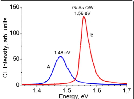
from the GaAs QW was not detected; only a wide lumi-nescence band at 1.48 eV, which could rather correspond to bulk GaAs, was observed as shown in the CL spectrum in the near-infrared (IR) region of Figure 1, where the CL emission A of the sample studied here is compared with
the peak B of the GaAs QW (1.56 eV at 77 K) observed in a similar structure but containing the normal InGaP-on-GaAs interface, i.e. GaAs substrate/GaAs buffer/ AlGaAs/GaAs/InGaP [12,13].
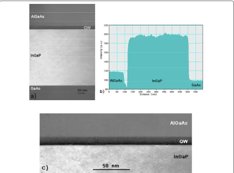
To check the reason for such anomalous emission, TEM (200) DF and STEM-HAADF were applied. Figure 2 shows the (200) DF TEM image of the sample. The nominal GaAs QW layer is the dark stripe between InGaP and AlGaAs. It exhibits a contrast darker than the GaAs substrate/buffer as seen in Figure 2b. This suggests that this layer is not GaAs. Figure 2c shows the high-magnification image of the nominal QW showing two different contrasts inside it in agreement with the profile of Figure 2b, confirming that the nominal QW is made up of two sublayers, as could also be concluded from Figure 2b. As the images were acquired in thin areas of the TEM specimen, the kinematical approxima-tion is used, according to which the (200) DF intensity
I200 is proportional to F2002 , withF200as the structure
factor of the (200) diffraction that depends on the atomic scattering factors f of the elements in the III-V compound as it isF200= 4(fIII- fV) [14-16]. To evaluate
composition, the DF contrast functionC200, which is
defined as the ratio between the (200) DF intensity dif-fracted by a given layer of general form AxB1-xCyD1-y
and that diffracted by GaAs, is used. An alloy looks dar-ker than GaAs when C200 is <1. C200 depends on the
square of the composition as does F2002 [14-16] because
fIII and fV have to be introduced in proportion to the
relative composition of the element they refer to. Computed plots of C200for InxGa1-xAs and GaAs1-yPy
are given in Figure 3. These plots show that these two alloys look darker than GaAs for x < 0.437 and y < 0.707, respectively. InxGa1-xAs1-yPy is also darker than
GaAs forx < 0.437 andy < 0.707 as is seen by similar plots; by way of example, only the plot for InxGa1-xAs 1-yPy with x = 0.1 is shown in Figure 3. No other alloy
has C200 < 1. Though (200) DF can clearly tell which
alloy had formed in place of the nominal GaAs QW at the inverted GaAs-on-InGaP interface, no exact estima-tion of the composiestima-tion is straightforward because of the square dependence of C200 on the composition and
the indication of just a composition range.
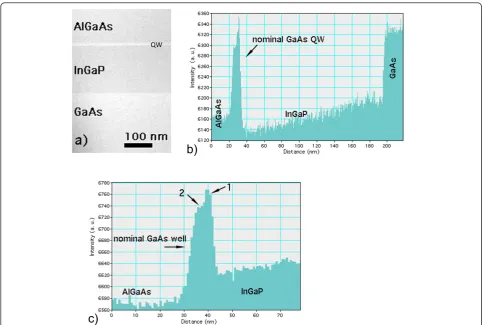
[image:2.595.58.291.509.681.2]To evaluate better the composition, the STEM-HAADF method was used. The STEM-HAADF image of the whole structure is given in Figure 4a. The intensity pro-file of Figure 4b shows that the contrast at the nominal GaAs layer is different from that of the GaAs substrate, confirming the DF results that the nominal QW is no longer made of GaAs. It also shows that the nominal GaAs well is made up of two sublayers, 1 and 2, with appreciable difference in HAADF contrast (Figure 4b,c); sublayer 1 (4 nm thick), which is closer to the GaAs-on-InGaP interface, with a contrast higher than the GaAs
substrate, and sublayer 2 (6 nm thick), which is on the side of the AlGaAs barrier, with a lower contrast.
The HAADF image is formed by collecting the inco-herently scattered electrons at high angles [17,18]. Single atoms scatter incoherently, and the image intensity is the sum of the individual atomic scattering contribu-tions [19]. The higher the atomic numberZ, the larger the scattering angle is. The HAADF intensity turns out to be proportional toZn,withn= 2 [17,18,20], so that a more direct evaluation of the composition is possible. Such dependence could also take other values for the exponent n, i.e. 1.7 <n< 2 [20]. Here it is assumed that
n = 2. This choice stems from the fact that only the exponent 2 can fully account for our experimental ratios of the intensities of every couple of layers of known composition in the structures (GaAs substrate/buffer, In0.51Ga0.49P, Al0.26Ga0.74As, taken as two by two) as
[image:3.595.58.539.88.442.2]shown in Figure 5, where the calculated HAADF QW
Figure 2(a) (200) DF TEM image of the sample and (b) intensity profile across it along the negative growth direction. In(a), the nominal GaAs QW is the dark stripe between InGaP and AlGaAs and corresponds to the downward peak between InGaP and AlGaAs in(b). The profile(b)clearly shows that it exhibits a contrast darker than the GaAs substrate/buffer (at the right-hand side).(c)High-magnification (200) DF image of the GaAs QW. The image has been treated with Adobe Photoshop to improve the visibility of the extra layer in proximity of the GaAs-on-InGaP interface.
0 1 2 3 4 5
0 0,2 0,4 0,6 0,8 1 1,2
x, y
(200
) DF contrast
C200
InxGa1-xAs
GaAs1-yPy In
0.1Ga0.9As1-yPy
Figure 3Calculated (200) DF contrast functionC200for InxGa
1-xAs (dash and dot line), GaAs1-yPy(solid line) and InxGa1-xAs
[image:3.595.58.292.518.690.2]intensity ratios for the two extreme cases ofn= 1.7 and
n = 2 are compared with the experimental ratios. The best agreement between the calculated rations and those of the experiment is obtained forn= 2.
The composition of the nominal GaAs QW is deter-mined from HAADF pictures by taking the known com-positions of the other alloys (GaAs substrate/buffer, In0.51Ga0.49P, Al0.26Ga0.74As) and related HAADF
inten-sity values as reference, i.e. as internal standards. The ratios of the experimental intensity of sublayers 1 and 2 to the intensity of all the inner standards are then com-pared to the calculated values of similar ratios for all the alloys that can be formed by combining together all the elements present at the inverted GaAs-on-InGaP inter-face assuming theZ2
dependence of the intensities. The ratio R of the HAADF intensity of a generic sublayer (subl) ApBqCr to the one of a generic standard (std)
EkFmGnis calculated from the equation:
R I A B C
I E F G
pZ qZ rZ
kZ m
p q r k m n
A B C
E
= = + +
+
HAADF subl
HAADFstd
( )
( )
2 2 2
2
Z ZF2+nZG2
(1)
c)
b)
[image:4.595.56.539.87.412.2]QW
Figure 4(a) STEM-HAADF image of the whole structure. The nominal GaAs QW is the bright stripe between the InGaP and AlGaAs barriers. (b,c)HAADF intensity profile across(a)and only across the nominal GaAs QW at higher magnification, respectively. Intensity scan along the negative growth direction. In(c), 1 and 2 indicate the two sublayers replacing the nominal GaAs QW (see text).
0,88 0,9 0,92 0,94 0,96 0,98 1 1,02
1 2 3
HAADF Intensity Ratio
n=1.7
n = 2
Exp.
Al
0.26Ga0.74As vs
GaAs
In
0.51Ga0.49P vs
GaAs
Al
0.26Ga0.74As vs
In
0.51Ga0.49P
[image:4.595.58.291.472.651.2]The alloy whose R matches the experimental ratio
Rexpis the one that a sublayer is made of.
The experimental ratiosRexpof the HAADF intensity
of sublayer 1 of the nominal GaAs layer to those of the GaAs substrate, In0.51Ga0.49P and Al0.26Ga0.74As, are
Rexp = 1.02, Rexp = 1.09 and Rexp = 1.12, respectively
(Table 1). For sublayer 2 of the nominal GaAs QW, the same ratios are 0.97, 1.03 and 1.06, respectively (Table 2). The compounds that exhibit ratio Rof their calculated intensities to GaAs substrate, In0.51Ga0.49P
and Al0.26Ga0.74As, in the same range as the
experimen-tal values given above are only InxGa1-xAs, GaAs1-yPy
and InxGa1-xAs1-yPy, which are in fairly good qualitative
agreement with (200) DF. The other alloys that may be formed at the inverted interface yield (much) different ratios for any possible composition.
Figure 6 is a worked-out example of the procedure used to extract information on the nature and composition of sublayers 1 and 2. Figure 6 is the plot of the calculated intensity ratio between In0.15Ga0.85As1-yPyand GaAs.
It shows that the experimental value ofRexp= 1.02 for
sublayer 1 can be accounted for if the layer is In0.15Ga0.85As0.81P0.19. A similar plot for InxGa1-xAs to
GaAs shows that In0.03Ga0.97As also fits the experimental
resultRexp= 1.02. The same procedure applied using the
In0.51Ga0.49P and Al0.26Ga0.74As layers as standards leads to
the same results for the stoichiometric indices, within 5%. By taking average values, it turns out that the sublayer 1 can be either In0.15Ga0.85As0.80P0.20or In0.023Ga0.977As. As
for sublayer 2 of the nominal GaAs QW, it results in either In0.05Ga0.95As0.84P0.16 or GaAs0.91P0.09 by the same
procedure.
The TEM results indicating the formation of InGaAsP at the location of the nominal GaAs QW are in qualita-tive agreement with an analogous conclusion drawn by CL in refs. [12,13], where a quaternary with the In com-position in the 0-0.15 range and the P one a little above zero was proposed. Both the TEM and CL results sug-gest that at the inverted GaAs-on-InGaP interface there is the formation of an extra quaternary layer of InGaAsP
inside the nominal GaAs QW (and partially replacing it), as also suggested in several studies [5,6,8-10,16,21]. The formation of just InGaAs as sublayer 1 might be less likely because it might easily happen that residual P atoms, which remained in the reactor after the PH3 flow
had been switched off, are incorporated in the first monolayers of the GaAs QW, since Ga prefers to bond to P rather than to As [22], as long as P atoms are avail-able (P/As intermixing mechanism, see later). Moreover, the absence of P in sublayer 1 would contradict its pre-sence in sublayer 2. On the other hand, the sequence inside the nominal GaAs QW such as layer 1 = In0.15Ga0.85As0.80P0.20 and layer 2 =
In0.05Ga0.95As0.84P0.16or GaAs0.91P0.09is congruent. In
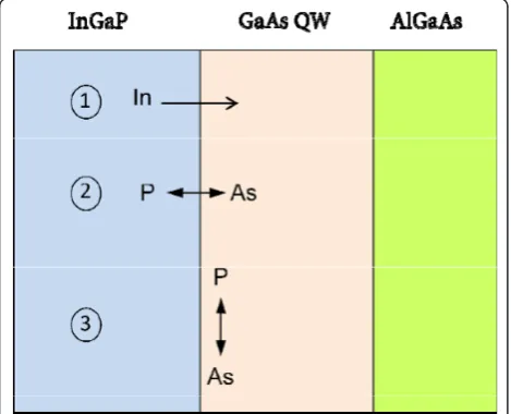
[image:5.595.55.539.113.157.2]fact, it matches the reasonable expectation that [In] and [P] decrease by moving away from InGaP, i.e. by going deeper into the nominal GaAs QW, while [Ga] and [As] increase. The stoichiometry of the sublayers 1 and 2 as determined by STEM-HAADF thus indicates a slight In and P enrichment of the nominal GaAs QW, which therefore changes its nature. Three mechanisms can cause such In and P enrichment, namely, In segregation in the growth direction, P/As exchange across the inter-face and P/As intermixing in proximity of the inverted interface, as discussed in other studies [5,6,8-10,16,21]. The three mechanisms are sketched in Figure 7. Indium surface segregation has been shown for other In-con-taining systems such as InGaAs/GaAs [23,24]. For the InGaP/GaAs system, the action of In segregation has been proven by experiments, showing that the growth of a thin GaP layer on the top of InGaP, before GaAs is grown, is effective in preventing the formation of the quaternary interlayer because In segregates into the interposed GaP layer and cannot reach the GaAs [5]. In segregates into the growing GaAs layer as soon as the latter starts to grow. In segregation is a kinetically dri-ven process and depends strongly on the growth tem-perature [5]. It may occur within the first few monolayers of the layer grown next [5,23,24]. P/As exchange across the interface should be excluded
Table 1 Values of the experimental ratioRexpof the HAADF intensityIHAADFof sublayer #1 to those of the three alloys (GaAs substrate, In0.51Ga0.49P and Al0.26Ga0.74As) contained in the sample and used as standards
I I HAADF HAADF Subl GaAs ( # ) ( ) 1 I I HAADF HAADF Subl
In Ga P
( # )
( . . )
1
0 51 0 49
I I
HAADF HAADF
Subl
Al Ga As
( # )
( . . )
1
0 26 0 74
[image:5.595.62.539.687.731.2]Rexp 1.02 1.09 1.12
Table 2 Values of the experimental ratioRexpof the HAADF intensityIHAADFof sublayer #2 to those of the three alloys (GaAs substrate, In0.51Ga0.49P and Al0.26Ga0.74As) contained in the sample and used as standards
I I HAADF HAADF Subl GaAs ( # ) ( ) 2 I I HAADF HAADF Subl
In Ga P
( # )
( . . )
2
0 51 0 49
I I
HAADF HAADF
Subl
Al Ga As
( # )
( . . )
2
0 26 0 74
according to our results. In fact, this mechanism would entail the incorporation of As in the bottom InGaP with the formation of some InGaAsP alloy inside the nominal InGaP layer, with the consequent broadening of the interface towards both the nominal InGaP and GaAs layers. These detailed investigations by chemically sensi-tive methods in a TEM right of the inverted interface do not confirm such symmetrical broadening and allow excluding the P/As exchange mechanism. The interface broadening towards only the top GaAs layer was observed by TEM also in other MOVPE-grown InGaP/ GaAs samples [16]. P/As intermixing occurs at the beginning of GaAs growth after the growth of InGaP
has finished. It consists in the fact that when the Ga and As fluxes are switched on to grow GaAs, some of the incoming Ga atoms bond to residual P atoms that are still remaining in the MOCVD chamber in contact with the sample surface after the PH3 flux has been
switched off. This is because the chemical bond strength of Ga-P is greater than that of Ga-As [22], which results in As substitution by P [9,22]. Such intermixing is lim-ited to the first monolayers of the growing nominal GaAs because the residual P atoms vanish out very quickly as no PH3 flux is active. As for In segregation,
P/As intermixing also depends on the substrate tem-perature which affects, e.g., the diffusion length of the P, As and Ga atoms on the growing surface. It also depends on the gas fluxes, on the application or non-application of a PH3-purging procedure or growth
inter-ruption [6]. Although the formation of an extra layer at the inverted interface during growth has been reported in a majority of the literature [5-10, 21 and references therein], its composition was seen to vary depending on the growth conditions used, as summarized above. In fact, it has been seen by photoluminescence that the emission associated with the extra layer spans quite a wide range, i.e. from 862 to 914 nm [5-10,21]. A major-ity of the published articles concluded that the extra layer is InGaAsP albeit with different compositions. Our results agree with this hypothesis. They also show that a finer structure may exist in the modified nominal GaAs QW, i.e. the presence of two sublayers: one more In-and P-rich layer closer to the undergrown InGaP layer and a second one that is less In and P rich farther from it. This structure is certainly due to the expected reduc-tion of P/As intermixing and In segregareduc-tion as the dis-tance from the inverted interface increases.
Conclusions
The deterioration of the structure of the GaAs QW in an InGaP/GaAs/AlGaAs heterostructure grown by MOCVD has been studied by CL and (S)TEM. The chemically sen-sitive (200) DF and HAADF methods of (S)TEM helped us to establish that the nominal GaAs QW has changed its structure, being replaced by two sublayers made of InGaAsP with different compositions. The sublayer clo-ser to the inverted GaAs-on-InGaP interface is more In and P rich than the one on the side of the AlGaAs-on-GaAs interface. The composition of the extra layer of InGaAsP closer to the inverted GaAs-on-InGaP interface, as determined by STEM-HAADF, reasonably accounts for the anomalous emission measured by CL. The forma-tion of the extra layers during growth was ascribed to the rearrangement of the atoms available at the inverted GaAs-on-InGaP interface caused by In segregation in the growth direction and P/As intermixing during the early stages of the GaAs QW growth.
0,6 0,7 0,8 0,9 1 1,1 1,2
0 0,2 0,4 0,6 0,8 1 1,2
I
(In
0.
15
Ga
0.
85
As
1-y
Py
) /
I
(Ga
As
)
y
In0.15Ga0.85As1-yPy /GaAs
0,95 1 1,05 1,1 1,15
0 0,05 0,1 0,15 0,2 0,25
I
(In
0.
15
Ga
0.
85
As
1-y
Py
) /
I
(G
aAs)
[image:6.595.56.291.88.251.2]y
Figure 6Plot of the calculated ratio R between the HAADF intensities of In0.15Ga0.85As1-yPyand GaAs. Inset is the top left part of the plot.
[image:6.595.57.292.482.672.2]Abbreviations
CL: cathodoluminescence; HAADF: high-angle annular dark field; MOCVD: metal organic vapour phase deposition; STEM: scanning TEM; TEM: transmission electron microscopy.
Author details 1
CNR-IMEM Institute, Parco Area delle Scienze 37/A, 43010 Parma, Italy2Ioffe Physical Technical Institute, 194021 Polytekhnicheskaya 26, Saint-Petersburg, Russia
Authors’contributions
CF made substantial intellectual contributions to the study. Carried out the TEM-HAADF, made the results interpretation and wrote the paper. AAS performed the measurement and interpretation of the cathodoluminescence results and revised the manuscript. DAV made the design and MOCVD growth of the heterostructures. MVZ supervised the work, participated in discussion of the results and in revising the manuscript.
Competing interests
The authors declare that they have no competing interests.
Received: 10 September 2010 Accepted: 3 March 2011 Published: 3 March 2011
References
1. Fu SI, Cheng SY, Lai PH, Tsai YY, Hung CW, Yen CH, Liu WC:’A Study of Composite-Passivation of an InGaP/GaAs Heterojunction Bipolar Transistor’.J Electrochem Soc2006,153:G938.
2. Wang CK, Yu KH, Chiou WH, Chen CY, Chuang HM, Liu WC:’On the high-performance n+-GaAs/p+-InGaP/n-GaAs high-barrier gate camel-like HFETs‘.Solid State Electron2003,47:19.
3. Bosi M, Pelosi C:’The Potential of III-V Semiconductors as Terrestrial Photovoltaic Devices’.Prog Photovolt Res Appl2007,15:51. 4. Lee CL, Wu MC, Lin W:’The influence of window layers on the
performance of 650 nm AlGaInP/GaInP multi-quantum-well light-emitting diodes’.J Cryst Growth1999,200:382.
5. Zhang XB, Ryou JH, Dupuis RD, Walter G, Holonyak N Jr:’Metalorganic Chemical Vapor Deposition Growth and Characterization of InGaP/GaAs Superlattices’.J Electron Mater2006,35:705.
6. Hsieh YC, Chang EY, Yeh SS, Chang CW, Luo GL, Chang CY, Lee CT: ’Optimization of the growth of the InGaP etch-stop layer by MOVPE for InGaP/GaAs HBT device application’.J Cryst Growth2006,289:96. 7. Kúdela R, Kučera M, Olejníková B, EliášP, Hasenöhrl S, Novák J:’Formation
of interfaces in InGaP/GaAs/InGaP quantum wells’.J Cryst Growth2000, 212:21.
8. Tsai CY, Moser M, Geng C, Härle V, Forner T, Michler P, Hangleiter A, Scholz F:’Interface characteristics of InGaP/GaAs double heterostructures grown by metalorganic vapor phase epitaxy’.J Cryst Growth1994, 145:786.
9. Guimarães FEG, Elsner B, Westphalen R, Spangenberg B, Geelen HJ, Balk P: ’LP-MOVPE growth and optical characterization of GaInP/GaAs heterostructures: interfaces, quantum wells and quantum wires’.J Cryst Growth1992,124:199.
10. Kwon YH, Jeong WG, Cho YH, Choe BD:’Effect of GaAsyP1-y(0≤y<1)
interlayers on the structural, optical, and electrical characteristics of GaAs/InGaP heterojunction’.Appl Phys Lett2000,76:2379.
11. Nittono T, Sugitani S, Hyuga F:’Photoluminescence characterization of InGaP/GaAs heterostructures grown by metalorganic chemical vapor deposition’.J Appl Phys1995,78:5387.
12. Shakhmin AA, Zamoryanskaya MV, Arsentyev IN, Konnikov SG, Vinokurov DA, Stankevich AL, Tarasov IS:’GaAs quantum well structures investigation by local cathodoluminescence’.Superlatt Microstruct2009, 45:376.
13. Konnikov SG, Gutkin AA, Zamoryanskaya MV, Popova TB, Sitnikova AA, Shakhmin AA, Yagovkina MA:’Integrated diagnostics of heterostructures with QW layers’.Semiconductors2009,43:1240.
14. Bithell EG, Stobbs WM:’Composition determination in the GaAs/(Al,Ga)As system using contrast in dark-field transmission electron microscope images’.Philos Mag A1989,60:39.
15. Petroff PM:’Transmission electron microscopy of interfaces in III-V compound semiconductors’.J Vac Sci Technol1977,14:973.
16. Frigeri C, Attolini G, Bosi M, Pelosi C, Germini F:’Parasitic Interlayer at the GaAs-on-InGaP Interface in MOVPE InGaP/GaAs: A Study by the Chemically Sensitive (200) Diffraction’.J Electrochem Soc2009,156:H448. 17. Pennycook SJ, Berger SD, Culbertson RJ:’Elemental Mapping with
Elastically Scattered Electrons’.J Microsc1986,144:229.
18. Pennycook SJ, Jesson DE:’High-resolution Z-contrast imaging of crystals’.
Ultramicroscopy1991,37:14.
19. Williams DB, Carter CB: InTransmission Electron Microscopy. Volume 3.New York: Springer; 1996, chap. 22.
20. Walther T:’A new experimental procedure to quantify annular dark field images in scanning transmission electron microscopy’.J Microsc2006, 221:137.
21. Sharma TK, Gokhale MR, Arora BM:’Long-wavelength photoluminescence from InGaP/GaAs heterointerfaces grown by metal organic vapour-phase epitaxy’.J Cryst Growth2000,213:241.
22. Decolbert J, Patriarche G:’Transmission electron microscopy study of the InP/InGaAs and InGaAs/InP heterointerfaces grown by metalorganic vapor-phase epitaxy’.J Appl Phys2002,92:5749.
23. Frigeri C, Di Paola A, Gambacorti N, Ritchie DM, Longo F, Giovanna MD: ’Transmission electron microscopy and X-ray diffraction investigation of In segregation in MOVPE-grown InGaAs-based MQWs with either GaAs or AlGaAs barriers’.Mater Sci Eng B1994,28:346.
24. Larive M, Nagle J, Landesman JP, Marcadet X, Mottet C, Bois P:’In situ core-level photoelectron spectroscopy study of indium segregation in GaInAs/GaAs heterojunctions grown by molecular-beam epitaxy’.J Vac Sci Technol B1993,11:1413.
doi:10.1186/1556-276X-6-194
Cite this article as:Frigeriet al.:Chemical characterization of extra
layers at the interfaces in MOCVD InGaP/GaAs junctions by electron beam methods.Nanoscale Research Letters20116:194.
Submit your manuscript to a
journal and benefi t from:
7 Convenient online submission 7 Rigorous peer review
7 Immediate publication on acceptance 7 Open access: articles freely available online 7 High visibility within the fi eld
7 Retaining the copyright to your article