OPTIMAL MAPPING MODE FOR XILINX
FIELD-PROGRAMMABLE GATE ARRAY DESIGN FLOW
1MEHDI JEMAI, 2SONIA DIMASSI, 3 BOURAOUI OUNI, 4ABDELLATIF MTIBAA
Laboratory of Electronic and microelectronic, University of Monastir, Monastir 5000, TUNISIA
E-mail: [email protected], [email protected], [email protected],
ABSTRACT
The design mapping mode has a large impact on FPGA designs in terms of performance, area, and power dissipation. Existing Xilinx FPGA design flow offers to designers three mapping modes. Each mode has its advantages and its drawbacks. To address this problem, in this paper, we have used these three Xilinx design mapping approaches to map set applications. Next, we have evaluated design results provided by each design mapping approach. Next, a comparative study between these design mapping modes has been presented. Finally, we have extracted the weak and the strong points of each design mapping mode.
Keywords: Design mapping mode; Xilinx FPGA device; FPGA Reconfiguration Zone; reconfigurable Module.
1. INTRODUCTION
Most users map the design on Field Programmable Gate Array (FPGA) without considering the location of the design on the FPGA device. This kind of mapping may degrade the design. However, in realty, the current Xilinx tools offer to designers three possibilities to map the design on the FPGA device [1],[2],[3].
1. Design mapping without FPGA
Reconfiguration Zone.
2. Design mapping with FPGA
Reconfiguration Zone using slice mode.
3. Design mapping with FPGA
Reconfiguration Zone using block mode.
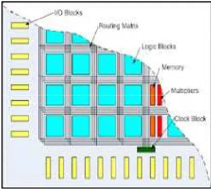
[image:1.595.303.512.429.618.2]The FPGA Reconfiguration Zone is the set of hardware resources used to execute a target design [4], [5], [6],[7]. It can be configurable logic blocks, arithmetic blocks, memory blocks, etc (show Fig.1). In this paper, we have explained how adding FPGA Reconfiguration Zone when mapping the design on the FPGA device. Furthermore, we have compared these three kinds of design mapping and we have showed the effect of the FPGA Reconfiguration Zone on the overall design. Finally, we have classified these design mapping modes in terms of resources, power and timing.
Figure 1: The FPGA Reconfiguration Zone
2. DESIGN MAPPING MODES
2.1 Design mapping without FPGA
Reconfiguration Zone
This kind of design mapping is the most easily and widely used by designers [8], [9]. According to this mode there are no FPGA area constraints when
reconfiguration zone is the entire FPGA. Hence, the design can spread over the entire of the FPGA device, (see Fig.2).
Figure 2: Design mapping without FPGA Reconfiguration Zone
2.2 Design mapping with FPGA
Reconfiguration Zone using slice mode
According to the slice mode, each FPGA Reconfiguration Zone can be modeled by a module. A module is rectangle with variable width and a fixed height. The slice mode requires the following design constraints [2],[4]:
The width of the module should be
necessarily a multiple of 4 slices.
The height of module should be equal to the
height of the target FPGA.
All logical resources (such as multipliers,
the slices, the RAM block, MAC, etc) covered by the module, considered a part of this module.
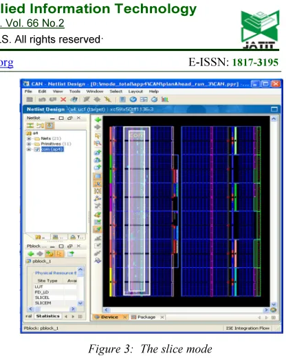
Xilinx has developed two tools called
[image:2.595.316.523.558.732.2]“Floorplanner” and “PlanAhead”. These tools allow the building of slice mode while respecting all design constraints shown above (see Fig.3).
Figure 3: The slice mode
The slice mode allows the optimization of material resources; however this mode suffers from many drawbacks. In fact, according to this mode user can build a very limit number of modules. In addition, design constraints required by this mapping mode are hard to meet in some cases.
2.3 Design mapping with FPGA
Reconfiguration Zone using block mode According to the block mode, each FPGA Reconfiguration Zone can be modeled by a module. A module is 2D rectangle with variable width and variable height. The block mode requires only one design constraint which the size of module. Indeed, the minimum size of module should be four slices [2]. This method is more flexible; indeed, it offers to designers the possibility to map several modules with different sizes. To build the block mode designer can use either “Xilinx Floorplanner tool” or “Xilinx PlanAhead tool”, (see Fig.4).
3. EXPERIMENTS
We have applied the three Xilinx design mapping approaches on several examples in different fields. We have chosen the following fields:
- Digital signal processing: our target
application was the Fast Fourier Transform
- Automotive & industrial: our target
application was the Controller Area Network
- Math Functions : our target application was
Pipelined Divider
- Video and Image processing : our target
application was the YCrCb to RGB color_space converter
- Communication and networking : our target
application was the Direct Digital Synthesizer
In our experiments, we have used the following tools: (i) Xilinx ISE version 12.1, (ii) Xilinx Xpower. These Xilinx design tools provide resources, power and timing reports incorporates timing delay, power dissipation and resources to provide a comprehensive area, power and timing summary of the design. Our target architecture was Xilinx virtex-5 running at 100 MHZ. Furthermore, these Xilinx design tools have executed under Windows-7 on Acer-PC (Intel Core 2 Duo T5500; 1.66 GHz; 1GB of RAM). In our experiment, we have compared design results in terms of: Resources utilization, (ii) timing, (iii) power dissipation.
3.1 Timing Design result
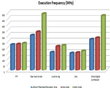
3.1.1 Execution frequency
[image:3.595.315.513.333.483.2]Xilinx synthesis tools offer to designers the execution frequency (Fex) of the target design. This means the value of frequency to be chosen to run the design. Hence, a mapping mode is classified to be good candidate if it increases the values of execution frequency.
Figure 5: Execution frequency (Fex)
Based on the above design results shown in Fig.5, we show that block mode is the best one in terms of execution frequency. Indeed, this mapping mode provides a gain by 32.30% compared to slice mode and by 44.65% compared to design mapping without FPGA Reconfiguration Zone. That’s why this mode should be chosen if designer looks to meet real time constraint.
3.1.2 Clock to pad times (offset-out)
[image:3.595.315.509.339.672.2]Xilinx synthesis tools to designers the offset out of all outputs of the target design. In fact, each output needs a delay after the clock event to be stable (definite), (see Fig.6). This delay is called offset out or clock to pad. Generally, a mapping mode is classified to be good if it reduces the values offset-out.
[image:3.595.319.500.503.676.2]Figure 6: Offset-out required time after clock
Figure 7: Minimum offset-out required time after clock
[image:3.595.97.287.578.730.2]compared to design mapping without FPGA Reconfiguration Zone. That’s why this mode should be chosen if designer looks to meet real time constraint.
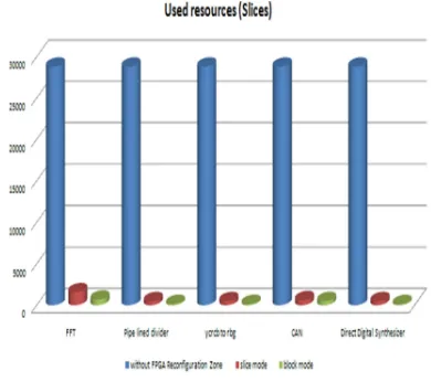
3.2 Resources Design results
[image:4.595.166.507.71.345.2]Design results shows (Fig.8) that the block mode is the best one, in fact, this mode uses less resource to implement compared to other modes.
Figure 8: Used resources
3.3 Power design results
The dynamic power Pd, depends on the logic used by the design and the frequency. It can write as [10]
Pd= A× C ×V2 × F (1)
Where: A: is the percentage of active logic gates, which are charged dynamically; C: is the total capacitance load; V: is the supply voltage; F: is the execution frequency.
[image:4.595.97.292.241.414.2]The equation 1 shows the dynamic power grows with the frequency; hence, based on Fig.5 the design mapping without FPGA Reconfiguration Zone should be the best one; indeed, this has been confirmed by design result shown in Fig.9. In fact, design mapping without FPGA Reconfiguration Zone consumes less power compared to 0.84% given by slice mode and 2.11% given by the block mode.
Figure 9: Total power
4. CONCLUSION
Recently, the need for efficient algorithms and design methods to minimize wasted server design parameters has become increasingly important. In this paper, we develop our research on comparing different design mapping mode offered by Xilinx. The hardware implementation was realized in virtex-5 using Xilinx design tools. The design results of the test and the simulation prove that the block mapping mode have a good impact on design. In fact, it improves the execution frequency and the used resource of the application, but it increases the power dissipated by the design. Furthermore, design results
show that the mapping without FPGA
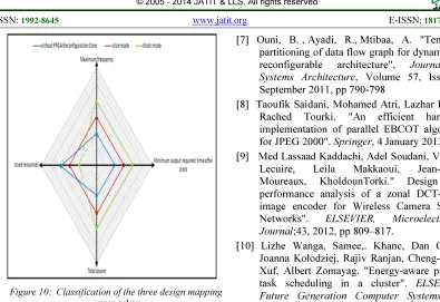
Figure 10: Classification of the three design mapping approaches
REFERENCES:
[1] Xilinx. Xilinx Partial Reconfiguration User
Guide. Xilinx User Guide UG702, April 26,
2013, (v14.5).
[2] Xilinx. Two Flows for Partial Reconfiguration:
Module Based or Difference Based. Xilinx
Application Note XAPP290, Sept 9, 2004,
(V1.2).
[3] Bouraoui Ouni, Ramzi Ayadi and Abdellatif Mtibaa, "Combining Temporal Partitioning and
Temporal Placement Techniques for
Communication Cost Improvement" Advances
in Engineering Software, Elsevier Publishers,
Volume 42, Issue 7, July 2011, pp : 444-451. [4] Tobias Becker, Markus Koester and Wayne.
Luk." Automated placement of reconfigurable
regions for reloadable modules". IEEE:
Circuits and Systems (ISCAS), 2010, pp
3341-3344.
[5] Ouni Bouraoui,.Mtibaa Abdellatif ." Online scheduling and placement of hardware modules
on partially dynamic architectures". Journal of
Circuits, Systems and Computers, Volume 22,
Issue 3, March 2013.
[6] P. Lysaght, B. Blodget, J. Mason, J. Young. "Enhanced architectures, design methodologies and CAD tools for dynamic reconfiguration on
XILINX FPGA. Bridgeford". In Proceedings
of the 16th International Conference on Field
Programmable Logic and Applications
(FPL06), Madrid, Spain, August 2006.
[7] Ouni, B. , Ayadi, R., Mtibaa, A. "Temporal partitioning of data flow graph for dynamically
reconfigurable architecture", Journal of
Systems Architecture, Volume 57, Issue 8,
September 2011, pp 790-798
[8] Taoufik Saidani, Mohamed Atri, Lazhar Khriji, Rached Tourki. "An efficient hardware implementation of parallel EBCOT algorithm
for JPEG 2000". Springer, 4 January 2013.
[9] Med Lassaad Kaddachi, Adel Soudani, Vincent
Lecuire, Leila Makkaoui, Jean-Marie
Moureaux, KholdounTorki." Design and
performance analysis of a zonal DCT-based image encoder for Wireless Camera Sensor
Networks". ELSEVIER, Microelectronics
Journal;43, 2012, pp 809–817.
[10] Lizhe Wanga, Samee,. Khanc, Dan Chena, Joanna Kołodziej, Rajiv Ranjan, Cheng-zhong Xuf, Albert Zomayag. "Energy-aware parallel
task scheduling in a cluster". ELSEVIER,
Future Generation Computer Systems; 29,