Technology (IJRASET)
Design Techniques For Low Power Implicit Pulse
Triggered Circuits
Smt.A.Rajani1, A.Yamini2 1
Assistant Professor, 2PG student, Department of ECE
University college of Engineering, Kakinada, A.P
Abstract - In Integrated circuits, the portion of the on chip power is covered by clock distribution network, flip-flops and latches. Flip flops and latches absorb large amount of power due to redundant transitions and clocking system. In this paper low power flops are presented. The single edge triggered conditional data mapping flop(CDMFF) and clocked pair shared flip-flop(CPSFF) are explained and compared with proposed flip-flop. The proposed flip-flop uses the double edge triggering technique by reducing the frequency to half. These flip-flops are simulated in HSPICE of 0.18μm CMOS technology with a power supply of 1.8V and a frequency of 50MHZ.
Keywords : Power; Flip-flops; CMOS circuit; CDMFF; CPSFF.
I. INTRODUCTION
In a synchronous digital system, the clock signal is used to specify a time reference for the movement of data within that system. Flip-flops are the primitive storage elements used in all types of digital circuit designs. The clock system, consists of the clock distribution network and sequential elements are one of the power consuming components in a VLSI system. It score for 30% to 60% of the total power dissipation in a system. As a result, reducing the power utilized by flip-flops will have a deep crush on the total power consumed. Conventional master slave flip flops are built up of two stages and are characterized by hard edge property. But pulse triggered flip flops lower the two stages into one stage and are characterized by soft edge property. Now a days pulse triggered flip flops have been expressed as an substitute to the conventional master-slave. Pulse triggered flip-flops can be distinguish into two types, implicit-pulsed and explicit-pulsed flip-flops. Caution must be paid to decrease the clock load when designing a clocking system. This paper is presented as follows: section II consists of techniques used in the flip-flops. Section III discusses the working of existing flip-flops succeed by proposed flip-flop in section. Section V presents the simulation results followed by conclusion in section VI.
II. TECHNIQUESUSEDINFLIP-FLOPS
Power utilization in the conventional CMOS digital circuit can be classified into three types (i) Static power (ii) Dynamic power and (iii) Leakage power . Although the static power has an significant part of total power, the dynamic power is also powerful in the total consumption. The dynamic power is calculated using the equation
Pd = Ceff V2f (1)
where f the frequency C the capacitance and V the supply voltage.
A. Single Edge Triggering
Figure 1: Single edge triggered flip-flop
The advantage of the D flip-flop is that the signal on the D input pin is taken at the moment, the flip-flop is clocked and subsequent changes on the input will be ignored until the next clock event.
B. Double Edge Triggering
[image:3.612.178.438.203.334.2]Both positive and negative edges are used to sample the D input at different clock edges, and the appropriate sample is selected for the Q output by a clocked multiplexer (MUX). The double edge triggering uses only half of the frequency of single edge triggering with same data throughput.
Figure 2: Double edge triggered flip-flop
As the frequency decreases, simultaneously power also
decreases.
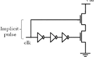
C. Implicit Pulse Flip-Flops
[image:3.612.227.388.439.535.2]In implicit type flip-flop, the pulse generator is a built in logic & there is no need for an external circuitry. Implicit flip-flop consists of 2 parts. a)clock distribution network b)latch for storage.
Figure 3: Implicit pulse flip-flop
It is more power efficient as pulses are produced internal to the circuit.
D. Reducing Clock Load Capacity
The clock load is reduced by minimizing the number of clocked transistors and the clock transistors consumes 100% switching activity. So, it necessary to reduce the power consumption consumed by clocked transistors.
III. WORKINGOFEXISTINGTECHNIQUESCDMFFANDCPSFF
A. Conditional Data Mapping Flipflop(CDMFF)
Technology (IJRASET)
Figure 4 : Conditional data mapping flip-flop
Initially when clk is low, node X is precharged to high. This circuit operates when clk and clk_b are high and it is evaluation period. Assume the previous state outputs for Q = 0, Qb_k = 1 and D = 1, so that the node X is discharged to gnd through N1, N3 and
N5 and make P3 ON pulling the output Q=1. The output remains high during evaluation period and also for clk = 0 and D = 0, since
all pull up and pull down paths are deactivated. When the flip-flop goes to evaluation period, and D = 0, the output Q is pulled down to 0 through N2, N4, and N5. When the flip-flop goes to evaluation period and the D input is low, the node X is not connected to Vdd
or gnd. So, the floating node exists. If a nearby noise occurs, discharges the node X as PMOS transistor P3 will be ON and a glitch
will appear on output node Q.
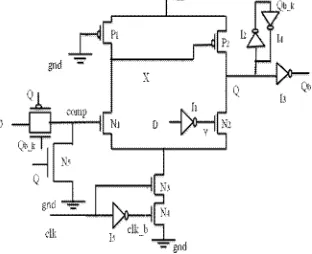
B. Clocked Pair Shared Flip-Flop (CPSFF)
Clocked pair shared flip-flop reduces the number the clocked transistors but eliminating the two PMOS precharge transistors with a single PMOS transistor which is always ON.
Figure 5: Clocked pair shared flip-flop
When clk and clk_b are at logic 1, circuit operates. Assume the previous state outputs for Q = 0, Qb_k = 1 and D = 1, N5 OFF andN1
is ON. The gnd voltage will pass throughN3 , N4 and N1 by making P2 ON pulling the output Q =1. When Q = 1, Qb_k = 0 and D =
0, N5 ON andN1 is OFF, then Q = 0 through N2 , N3 and N4. This flip-flop depends on previous output Q and Qb_k in addition with
clk and data input. When D = 1, N5 is idle. When D = 0, transmission gate is idle. In high frequency operation the transmission gate
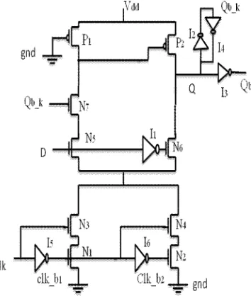
[image:4.612.228.384.469.596.2]A. Implicit Pulse Dual Edge Triggered Flip-Flop
In this, clock branch sharing scheme (N1, N3) (N2, N4) are joint by the first stage and second stage. A split path (node X does not drive NMOS N6 of the second stage, which is used in the output discharging path) is used to ensure the correct functioning after merging. The advantage of this sharing is reflected in reducing the number of transistors required to implement the clocking branch. Before the circuit goes to evaluation period, node X precharges to high, as the PMOS is connected to gnd. During evaluation period assuming the previous state outputs Q = 0, Qb_k = 1 and D = 1, N1 , N3 are ON. Node X discharges to gnd through N7 , N5 , N3 , N1.
[image:5.612.219.396.200.409.2]So, X goes to low and P2 is ON the outputs are Q = 1 ,Qb_k = 0.
Figure 6: Double edge triggered flip-flop
Again when the circuit goes to evaluation period, Q = 1, Qb_k = 0 and D = 0, N2 , N4 are ON. The output Q is pulled down to 0 i.e Q
= 0, Qb_k = 1. An inverter is placed after Q, providing protection from direct noise coupling.
V. SIMULATIONRESULTS
The simulation results were performed with a voltage of 1.8v and frequency of 50MHZ. For the simulation results, X-axis is time period in nano seconds (ns) and Y-axis is voltage in volts (v).
[image:5.612.180.425.518.715.2]Technology (IJRASET)
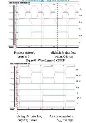
Previous state o/p clk high & data low, taken as 0 output Q is low
Figure 8 : Waveforms of CPSFF
clk high & data low, As X is connected to output Q is low Vdd, it is high
[image:6.612.152.445.71.490.2]Figure 9 : Waveforms of Double edge triggered flip-flop.
Table 1: Comparison in terms of power
Power
(uW) 100MHZ 50MHZ 25MHZ
CDMFF 202.4125 136.1937 128.8094
CPSFF 176.3897 127.9494 117.7126
DET 158.4481 106.4735 102.3993
0 50 100 150 200 250
100MHZ 50MHZ 25MHZ
[image:7.612.197.423.93.228.2]CDMFF CPSFF DET
Figure 10 : Power analysis of flip-flops at different frequencies From the above comparison, the power decreases as the frequency decreases.
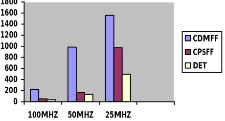
Table 2: Comparison in terms of delay (TPD) TPD
(pS) 100MHZ 50MHZ 25MHZ
CDMFF 223.0081 985.5619 1557.4208
CPSFF 53.6805 167.5739 972.8790
DET 35.8686 133.5619 497.1721
In below bar diagram, X-axis is frequency in mega hertz (MHZ) and Y-axis is delay in Pico seconds (pS)
0 200 400 600 800 1000 1200 1400 1600 1800
100MHZ 50MHZ 25MHZ
CDMFF CPSFF DET
Figure 11: Delay analysis of flip-flops at different frequencies
[image:7.612.195.425.387.511.2]It is observed that, as the frequency decreases, the delay increases.
Table 3: Comparison in terms of power delay product (PDP)
PDP
(fJ) 100MHZ 50MHZ 25MHZ
CDMFF 67.7117 737.534 1164.5675
CPSFF 57.7799 209.3834 631.8902
Technology (IJRASET)
In the below bar diagram, X-axis is frequency in mega hertz (MHZ) and Y-axis is power delay product in femto Joules(pJ)
0 200 400 600 800 1000 1200 1400
100MHZ 50MHZ 25MHZ
CDMFF CPSFF DET
Figure 12 : Power delay product analysis of flip-flops at different frequencies.
As the frequency decreases, the power delay product increases but the DET has less than the other two circuits.
VI. CONCLUSION
The design of Single edge and dual edge circuits are outlined and are simulated. It is observed that the as the frequency decreases power decreases and the delay, power delay product increases. The proposed design has achieved low power and better power delay product than the existing architectures.
VII. ACKNOWLEDGEMENT
I express my profound sense of gratitude to my guide Smt. A. Rajani Assistant Professor, JNTU Kakinada for her systematic guidance and valuable advices. I would like to express my sincere gratitude to Dr.A.M.Prasad, Professor, Head of the Department and Dr.K.Babulu, Professor, course coordinator, for providing me with all necessary facilities for the work.
REFERENCES
[1] Peiyi Zhao, Jason McNeely, Weidong Kuang, Nan Wang, and Zhongfeng Wang ,” Design of Sequential Elements for Low Power Clocking System” , IEEE Trans. Very Large Scale Integr. (VLSI) Syst., Vol. 19, no. 5, May 2011.
[2] P. Zhao, J. McNeely, P. Golconda, M. A. Bayoumi, W. D. Kuang, and B. Barcenas, “Low power clock branch sharing double-edge triggered flip-flop,” IEEE Trans. Very Large Scale Integr. (VLSI) Syst., vol. 15, no. 3, pp. 338–345, Mar. 2007.
[3] S. Lin, H. Z. Yang, and R. Luo, “High speed soft-error-tolerant latch and flip-flop design for multiple VDD circuit,” in Proc. IEEE Int. Comput. Soc. Annu. Symp. VLSI (ISVLSI), pp. 273–278, Mar. 2007.
[4] C. K. Teh, M. Hamada, T. Fujita, H. Hara, N. Ikumi, and Y. Oowaki, “Conditional data mapping flip-flops for low-power and high-performance systems,” IEEE Trans. Very Large Scale Integr. (VLSI) Syst., vol. 14, no. 12, pp. 1379–1383, Dec. 2006.
[5] J. Tschanz, S. Narendra, Z. P. Chen, S. Borkar,M. Sachdev, and V. De, “Comparative delay and energy of single edge-triggered & dual edge triggered pulsed flip-flops for high-performance microprocessors,” in Proc. ISPLED, Huntington Beach, CA, pp. 207–212, Aug. 2001.
[6] C. L. Kim and S. Kang, “A low-swing clock double edge-triggered flip-flop,” IEEE J. Solid-State Circuits, vol. 37, no. 5, pp. 648–652, May 2002.
[7] P. Zhao, J. McNeely, S.Venigalla, G. P. Kumar,M. Bayoumi, N.Wang, and L. Downey, “Clocked-pseudo-NMOS flip-flops for level conversion in dual supply systems,” IEEE Trans. Very Large Scale Integr. (VLSI) Syst., to be published.