EFFECT OF Zn DOPING ON In2Se3 THIN FILMS FOR PHASE CHANGE RANDOM ACCESS MEMORY (PRAM) APPLICATIONS
OPIYO SAMWEL OLAKA (BEd (Sc)) REG.NO. I56/CE/22404/10
DEPARTMENT OF PHYSICS
A thesis submitted in partial fulfillment of the requirements for the award of the Degree
of Masters of Science (Electronics and Instrumentation) in the school of Pure And
Applied Sciences of Kenyatta University
DECLARATION
I declare that the work presented in this thesis is my original work and has not been
presented for the award of a degree or any other award in any other University.
Signature………..Date……….………
OPIYO SAMWEL OLAKA I56/CE/22404/2010
This thesis has been submitted for examination with our approval as University Supervisors
DR. W.K. NJOROGE
Signature………..Date……….………
DEPARTMENT OF PHYSICS
KENYATTA UNIVERSITY
DR. M. K. MUNJI
Signature………..Date……….………
DEPARTMENT OF PHYSICS
Dedication
Acknowledgement
My special and sincere gratitude go to my supervisors Dr. W. K. Njoroge and Dr. M.K.
Munji for their unlimited scholarly guidance and encouragement during the research
work. Their vast knowledge in thin films and electronics research was a great
contribution to the success of this work. I thank them for their willingness to see this
thesis through to the end.
I am grateful to the entire staff of Physics Department Kenyatta University for being
supportive throughout the research period. Special thanks go to Mr. Chisaina Abraham of
Kenyatta University, Mr. Odek Felix of Kisumu Polytechnic and Prof. Oduor Andrew of
Maseno University for their tireless support during my laboratory work. May I also
extend my appreciation to Mr. Muthoka Bonface of University of Nairobi, Chiromo
campus, and the International Science Programs (ISP) of Uppsala University, Sweden
due to their support to the University of Nairobi Department of Physics labs where I
carried out part of my laboratory work.
Gratitude to my parents and siblings for their emotional and financial support during the
period of my study. I salute my colleagues Nyakiti Kevin, Otieno Phylip, Koros Hosea
and Muchira Irene just to mention but a few for their constant support and encouragement
at the time of need.
Finally and most importantly, I would like to sincerely thank The Almighty God for His
Table of Contents
Declaration... ii
Dedication ... iii
Acknowledgement ... iv
Table of Contents ...v
List of tables...x
List of figures ... xi
List of Acronyms and Abbreviations ... xiii
Abstract ...xv
CHAPTER ONE ...1
INTRODUCTION ...1
1.1 Background to the study ... 1
1.2 Problem Statement and Justification ... 3
1.3 Objectives ... 3
1.3.1 General Objective ... 3
1.3.2 Specific Objectives ... 4
1.4 Rationale ... 4
CHAPTER TWO ...6
LITERATURE REVIEW ...6
CHAPTER THREE ...12
THEORETICAL CONSIDERATIONS ...12
3.1 Introduction ... 12
3.2 Thin Film Deposition Methods ... 12
3.2.1 Evaporation ... 13
3.2.2 Sputtering technique ... 15
3.3 Electrical resistivity in semiconductors ... 20
3.3.1 Thin film sheet resistivity ... 22
3.4 Phase Change Random Access Memory ... 24
3.4.1 Set /Reset Operations... 24
3.4.2 Resistance-current (R-I) curves ... 28
3.4.3 I-V curves. ... 28
3.4.4 Reliability Considerations ... 29
3.5 Other Memory Technologies Currently In the Market ... 31
3.5.1 Static Random Access Memory (SRAM) ... 31
3.5.2 Dynamic Random Access Memory (DRAM) ... 33
3.5.3 Flash Memory ... 35
3.5.4 Ferroelectric Random Access Memory (FeRAM) ... 39
3.5.5 Magnetoresistive Random Access Memory (MRAM) ... 40
EXPERIMENTAL PROCEDURE ...41
4.1 Introduction ... 41
4.2 Zn:In2Se3 alloys synthesis and thin film deposition ... 41
4.3 Determining electrical properties using four point probe ... 43
4.4 Sheet resistance determination during thermal cycling ... 44
4.5 Fabrication of a PRAM ... 45
4.6 Characterization of the PRAM ... 45
4.6.1 DC current sweep test ... 46
4.6.2 Pulsed mode test ... 47
CHAPTER FIVE ...50
RESULTS AND DISCUSSION ...50
5.1 Introduction ... 50
5.2 Determination of Thin Film Thickness ... 50
5.3 Determination of Sheet Resistance for Amorphous and Crystaline Thin Films ... 51
5.3.1 Variation of as deposited sheet resistance with Zinc doping levels ... 52
5.3.2 Variation of Sheet Resistance with Zinc doping for the annealed samples ... 53
5.4 Sheet Resistance Variation During Thermal Cycling ... 54
5.4.1 Variation of sheet resistance with temperature for 0% Zn doping ... 55
5.4.2 Variation of Sheet Resistance with Temperature for 2% Zinc Doping ... 56
5.4.4 Variation of sheet resistance with temperature for 6% Zinc doping ... 57
5.4.5 Variation of sheet resistance with temperature for 8% Zinc doping ... 57
5.4.6 Comparison of R- T curves for different Zinc doping percentages on In2Se3 .. 58
5.5 Variation of Crystallization Temperature with Zinc Doping ... 60
5.6 Variation of resistance contrast with increase in Zinc doping levels ... 64
5.7 Sheet resistivity for Amorphous and crystalline films for Zn:In2Se3 and GST. .... 66
5.8 Determination of activation energy for 4% Zn doped sample ... 68
5.8.1 Kissinger method ... 69
5.8.2 Augis-Bennett Approximation ... 71
5.9 Electrical characterization of the PRAM ... 73
5.9.1 DC test (Current Sweep)... 73
5.9.2 Pulsed mode testing of the PRAM. ... 75
CHAPTER SIX ...78
CONCLUSIONS AND RECOMMENDATIONS ...78
6.1 Conclusions ... 78
6.2 Recommendations ... 79
REFERENCES ...81
APPENDICES ...86
Appendix I: Photograph of Edwards Auto 306 vacuum coater. ... 86
List of tables
Table 3.1: Basic attributes of emerging memory technology (Ping, 2012) ... 34
Table 5.1: Film thickness from FTM6 and scout software for Zn:In2Se3……….51
Table 5.2: Amorphous and Crystalline Sheet Resistance for Zn:In2Se3 Thin Films ... 52
Table 5.3: Crystallization temperature for In2Se3 at different Zinc doping levels ... 62
Table 5.4: Ratio of Amorphous and crystalline resistances for Zn:In2Se3 Films ... 65
Table 5.5: Sheet resistivity for Amorphous and Crystalline Zn:In2Se3 and GST ... 67
Table 5.6: Crystallization parameters for 4% Zn:In2Se3 using Kissinger’s method. ... 69
List of figures
Figure 3.1: Schematic diagram of thermal evaporation system. ... 13
Figure 3.2: Sputtering phenomenon (Matsunami et al., 1980) ... 16
Figure 3.3 (a): Schematic diagram of DC sputtering set up (Ohring M, 1992) ... 18
Figure 3.3 (b): Schematic diagram of RF sputtering set up (Ohring M, 1992) …………19
Figure 3.4: Four point probe tips on a thin film (Agumba et al., 2012) ... 22
Figure 3.5: Simple structure of a PRAM cell (Ping , 2012) ... 25
Figure 3.6: SET / RESET operations of a PRAM (Barclay, 2009) ... 26
Figure 3.7: Schematic diagram of SRAM cell (IBM 1997)... 31
Figure 3.8: Schematic Diagram of a DRAM Cell (Zilberberg et al., 2013) ... 34
Figure 3.9: Schematic diagram of a NOR Flash architecture (Elnec, 2008) ... 37
Figure 3.10: Schematic diagram of NAND Flash architecture (Elnec, 2008) ... 38
Figure 4.1: Set up for Zn:In2Se3 alloy formation………..42
Figure 4.2: Set up used in sheet resistivity measurement (Agumba, 2010) ... 43
Figure 4.3: Set up for thermal cycling ... 44
Figure 4.4: Schematic diagram of PRAM cell. ... 45
Figure 4.5: Set up for I-V testing ... 46
Figure 4.6: Block diagram of the set up for SET/RESET operation. ... 48
Figure 5.1: Graph of variation of amorphous resistance with %Zn doping levels….…...52
Figure 5.2: Graph of variation of the sheet resistance for Zn:In2Se3 crystalline films ... 53
Figure 5.3: R-T curves for different levels of zinc doping on In2Se3 ... 55
Figure 5.4: Sheet Resistance Vs Temperature graph (between 200OC to 230 OC) ... 60
Figure 5.6: Variation of Crystallization temperature with % zinc doping ... 63
Figure 5.7: Graph of resistance contrast with increase in % Zn doping ... 65
Figure 5.8: R-T curves for 4% Zn doped In2Se3 at varied heating rates ... 68
Figure 5.9: The Kissinger plots for 4% Zn doped In2Se3. ... 70
Figure 5. 10: The Augis-Benett plots for 4% Zn doped In2Se3 ... 72
Figure 5.11: I-V curve for 4% Zn-In2Se3 PRAM ... 74
Figure 5.12: RESET Pulsed-mode switching behavior of Zn:In2Se3 PRAM ... 75
List of Acronyms and Abbreviations
CMOS Complementary Metal Oxide Semiconductor
CVD Chemical Vapor Deposition
DRAM Dynamic Random Access Memory
DUT Device-Under-Test
EEPROM Electrically Erasable Programmable Read-Only-Memory
EM Electro-Magnetic
FeRAM Ferroelectric Random Access Memory
GST Germanium Antimony Telluride
GT Germanium Telluride
I-V Current – Voltage
In2Se3 Indium Selenide
MRAM Magneto Resistive Random Access Memory
NVM Non-Volatile Memory
PCM Phase Change Material
PRAM /PCRAM Phase-Change Random Access Memory
PVD Physical Vapor Deposition
R-I Resistance-Current
R-T Resistance-Temperature
R-Vs Resistance- Voltage (SET)
R-VR Resistance –Voltage (RESET)
SCCM Standard Cubic Centimeter per Minute
ST Antimony-Tellurium alloy
Tc Crystallization temperature
TEM Transmission Electron Microscopy
Zn Zinc
Abstract
CHAPTER ONE
INTRODUCTION
1.1 Background to the study
The idea of using amorphous to crystalline phase transition of chalcogenides for an
electronic memory technology has been pursued for many years (Ovshinsky, 1968).
Phase Change Random Access Memory (PRAM) is a non volatile memory that employs
the reversible phase change in material to store bits of information (Wong et al., 2010). PRAMs have desirable characteristics including, fast switching speed, low programmable
energy, high endurance, good data retention, improved compatibility with CMOS and
excellent scalability (Qiao et al., 2006). Studies have also shown that PRAM cycling
endurance is of the order 108 writes (the number of successive write/erase cycles before the cell fails) which is significantly higher than that of floating gate technology which is
reported to be approximately 105 (Gleixer et al., 2009). In addition PRAM is capable of creating new functions and applications of its own which are fast write programming
speed and direct overwrite capability (Daewon and Kinam,2007).
Generally PRAM utilizes the large resistivity contrast between crystalline (low
resistivity) and amorphous (high resistivity) phases of the Phase Change Material (PCM).
The SET and the RESET states of the PCM refer to low and high resistance respectively.
finite time to fully crystallize the amorphous region (Wong et al., 2010). Many
researchers have widely studied Ge2Sb2Te5 (GST) and optimized it for PRAM
applications. However GST has been reported to have some drawbacks for instance,
meta-stable face centered cubic (fcc) structure, low crystallization temperature and low
crystallization resistance. The low crystallization temperature means it is unable to retain
data at high temperature. To eliminate these problems, a new PCM for next generation
PRAM applications must have a higher crystallization temperature and also higher
crystalline resistance with a faster phase change speed than GST.
The area of application of the PRAM determines its operation temperature. Embedded
memory applications operate at 85oC while automotives operate at 150oC. (Wong et al., 2010). Research has shown that crystallization temperature is directly proportional to the
data stability while crystalline resistance is inversely proportional to the RESET
operation power (Heon and Dae-Hwan, 2005). It is therefore necessary to come up with a
material that has high crystallization temperature and also high crystalline resistance.
This will ensure an improved data retention capability and reduce the RESET power of
the PRAM.
It has been reported that additives for instance Zinc, Silicon dioxide, Titanium, Nitrogen
among others have the ability to influence the crystallization temperature of PCM. For
instance crystallization temperature of GST increases with increase in SiO2
temperature and activation energy for crystallization of GeTe (Ramesh et al., 2011; Sousa
et al., 2011). Selenium has been found to have tremendous potential in device technology since it exhibits a unique property of reversible transition. Additives increase the
hardness, sensitivity and crystallization temperature of selenium as well as lessening the
ageing effect (Sushama et al., 2006).
1.2 Problem Statement and Justification
The conventionally used compound for PRAM application, Ge2Sb2Te3, has been found to
have some limitations including, low crystallization temperature and low crystalline
resistance. These characteristics of GST make it have low data retention ability as well as
high RESET power. It is therefore necessary to research on a compound that will
eliminate these limitations and bring in more desirable characteristics of PRAM (Bastard
et al., 2011). In2Se3 has been given little attention despite it showing better results when doped with additives like Nitrogen and lead. This study was aimed at finding out the
effects of Zinc doping on electrical characteristics of In2Se3.
1.3 Objectives
1.3.1 General Objective
The main objective of this study was to deposit In2Se3 thin film doped with different
ratios of Zinc by mass using vacuum evaporation technique and determine their electrical
1.3.2 Specific Objectives
The specific objectives of this study were to:
(i). Synthesize alloys of In2Se3 doped with Zn at different composition by mass.
(ii). Deposit Zn doped In2Se3 thin films on glass substrate by employing
evaporation technique using Edward Auto 306 RF/DC vacuum evaporation
chamber.
(iii). Investigate the influence of Zn doping on the electrical characteristics of
In2Se3 thin films using four point probe interfaced with a computer running a
LabVIEW program.
(iv). Fabricate and electrically characterize a PRAM prepared using the optimized
material.
1.4 Rationale
With the growing applications of digital electronic device such as smart phones, digital
cameras and Mp3 players among others, the need for a high switching speed non volatile
semiconductor memory is inevitable. In addition, today‘s high performance computing
requires non-volatility of memory. This has led researchers to try and find the new
technologies and materials to build a nonvolatile RAM which has fast switching speed,
dense, low power consumption and economically favorable (Pronin, 2011). Presently
Flash memory which has a number of practical problems such as scaling difficulties as
chip lithography shrinks is one of the commonly used non volatile memory. There is
PRAM which is a non volatile memory has additional advantages over the conventional
Flash memories for instance; it has extremely large read dynamics range, reduced
switching current as well as improved device size. This study was aimed at investigating
CHAPTER TWO
LITERATURE REVIEW
2.1 Related Studies
A number of researchers (Friedrich et al., 2000; Heon et al., 2005; Guoxing et al., 2012) have investigated different materials for PRAM applications including Ge2Sb2Te5,
Si-Sb-Se, SnSi-Sb-Se, InSe among others. These studies were geared towards discovery of a PRAM
that is fast switching, utilizes less current and has high data retention ability. It is from
their work that the information on the promising materials, techniques and methods that
will lead to getting a better performing PRAM is obtained. In this section we appreciate
the work that other researchers have done in this field as we look at the possibility of
improving their work.
Bin et al. (2007) in their study on Indium selenide nanowire phase change memory,
successfully fabricated PRAM with a better switching behavior. They obtained a
resistance of about 5 orders of magnitude with the crystalline resistance being relatively
higher than the conventional GST. This translated to lower RESET power. They applied
7V, 20ns pulse and 5V, 100𝜇𝑠 pulse for RESET and SET states respectively. However in
their study there was no attempt to introduce an additive to the PCM which might have
reduced the RESET power even further. Guoxing et al. (2012) studied Phase change behavior of zinc doped GST film and observed that Zn15.16(Ge2Sb2Te5)84.84 phase change
about 0.78 eV, better data retention of 10 years at 167.5 0C, higher crystalline resistance and faster crystallization speed compared with the conventional Ge2Sb2Te5. Heon et al. (2005) studied switching behavior of indium selenide and discovered that In2Se3 PRAM
has a much higher electrical resistivity than the GST. The resistivity also varied by a
factor of 105 which is higher than the GST. The high resistivity demonstrated low RESET power for the RAM. However, In2Se3 being a binary compound and has no chance of
achieving multi-bit cell. Bletskan (2005) studied Glass formation and crystallization in
the system Ge-Te by depositing GeTe alloy using magnetron sputtering method. The
electrical and thermal characteristics of the film were investigated. Though the material
showed phase transition, it was however noted that GeTe exhibited too low
crystallization temperature. This is an undesirable characteristic since it demonstrates that
the PRAM has low retention capability. Kim et al. (2010) presented results of a highly scaled PRAM cell with sufficiently high cycling endurance and fast programming speed
as well as small cell size to potentially challenge DRAM in future applications. This
PRAM cell showed potential to overcome the technology limitation of DRAM cell below
20 nm technology node. This cell however had retention duration of 4.5 years at a
temperature of about 85oC.
Qiao et al. (2006) in their study on the performance of GST material for PRAM devices,
compared the characteristics of GST and Silicon doped SbSe. They found that the
resistivity ratio of Si-Sb-Se increased to reach 106 during amorphous-crystalline transition. The melting point of Si-Sb-Se was however found to be lower than that of
were relatively smaller as compared to GST. Simon et al. (2011) investigated the effects
of dopants namely Nitrogen, Silicon, Tin and Aluminum oxide on GST and GT
compounds. The films were deposited using co-sputtering technique. From the research it
was reported that Nitrogen had desirable effects on GST as it increased the crystallization
temperature as well as the crystalline resistance. On the other hand Tin raised the
crystallization temperature of GT but reduced its electrical constants. Silicon was also
reported to have raised the crystallization field of GT from 143 to 149V/𝜇𝑚.
Lee et al. (2010) researched on switching behavior of indium selenide phase change
memory cell. The experiment was performed under the static dc test, switching mode for
a 5 𝜇𝑚 size In2Se3 PRAM. In the initial sweep the as grown amorphous In2Se3 showed
high resistance state at low voltage region. However, when it reached the threshold
voltage the electrical resistance of the device was drastically reduced due to the formation
of an electric conducting path. The pulse mode switching of the In2Se3 showed that the
RESET of the device was done with a 70 ns – 3.1 V pulse and the SET state of the device
was obtained by 10 𝜇𝑠 - 1.2 V pulse. This represented a high switching dynamic range
ratio (Rhigh to Rlow) of about 100.
Most of the work done by other researcher has led to the discovery of better materials for
PRAM applications, though the very desirable properties like high crystallization
temperature, high crystalline resistance, high switching speed and low switching power
doping on the Phase change properties of In2Se3. Zn doping has shown remarkable results
with chalcogenide compounds for instance raising the crystallization temperature of
Se-Ge (Deepika et al., 2012). In2Se3 has shown better electrical characteristics when doped with Nitrogen and Carbon. Xiang et al. (2013) studied enhanced thermal stability and
electrical behavior of Zn-doped Sb2Te films for phase change memory applications and
discovered that Zn atoms significantly increase crystallization temperature of
Znx(Sb2Te)1-x film. They carried out the study with the percentage atomic weight of zinc
ranging from 0 to 29.67 at. %. Zinc doping also improved crystalline resistance that
would eventualy lower the RESET power of a PRAM. The best compositions were
Zn26.07(Sb2Te)73.93 and Zn29.67(Sb2Te)70.33 films since they exhibited large resistance
change, faster crystallization speed and better thermal stability due to the formation of
amorphous Zn-Sb and Zn-Te phases as well as uniform distribution of Sb2Te crystalline
grains.
Etefagh et al. (2013) studied Effect of Zn doping on optical properties and
photoconductivity of SnS2 nanocrystalline thin films. They employed spray pyrolysis
method of thin film deposition. The doping level was changed from [Zn/Sn] = 0 to 7·5
at%. The films were characterized by means of X-ray diffraction, scanning tunneling
microscopy (STM), energy dispersive X-ray analysis (EDX), photoluminescence and
UV-VIS spectroscopy. They reported that Zn insertion causes a significant decrease in
grain size. Optical band gap of the films were calculated for different dopant
discovered that the sensitivity to the light increases by zinc incorporation, which was a
large amount for SnS2:Zn of 7·5%.
Gu et al. (2012) studied SixSb2Te materials with stable phase for PRAM applications.
They looked at the physical and electrical properties of SixSb2Te system materials at
various Si contents and discovered that SixSb2Te showed better thermal stability than
Ge2Sb2Te5 due to the fact that there was no Te separation under high annealing
temperatures. The increase of Si content therefore enhanced the data retention ability of
SixSb2Te materials. When the value of x was increased to more than 0.44, the 10-year
data retention temperature for SixSb2Te exceeded 110 oC, which meets the long-term data retention requirement. Furthermore, Si-rich Sb2Te materials exhibited the improvement
on thickness change after annealing compared with Ge2Sb2Te5. In addition, the PCRAM
devices based on SixSb2Te (x = 0.31, 0.44) were fabricated and the electrical operations
were carried out. Both of them showed the outstanding performances with long-term
operations.
Kamau (2013) studied Nitrogen doping effect on tin-selenium thin films for phase change
memory applications. Films of N- SnSe were deposited at room temperature on glass
substrates using reactive thermal evaporation. Threshold switching was observed in the
films with resistivity dropping by 5 orders of magnitude. Increasing nitrogen
concentration led to a more complex XRD pattern due to formation of multiphase of
0 sccm N to 3.57 eV at 1 sccm N. The resistivity of the thin film decreased from 1280 –
1150 Ωcm and 9.3 - 0.3 Ωcm for amorphous and crystalline N-SnSe films respectively.
The fabricated PRAM cell had threshold switching voltage, Vth, of 4.47 V at a current
1.04 mA.
Muchira (2013) studied crystallization kinetics of InxSey thin films prepared by vacuum
evaporation for PRAM applications. In this work crystallization kinetics of different
ratios of InSe was investigated. After evaporation, Lindberg tube furnace and Keithley
sourcemeter were employed for insitu annealing and resistivity measurement
respectively. In40Se60 (In2se3) which had the highest activation energy of 0.538 ± 0.063eV
was the best for PRAM application since it was giving a lot of space for the PRAM
scaling. However this material registered lower crystallization temperature which
translated to high data instabilities.
It is clear from the discussion of the previous studies that most of the alloys employed in
PRAM fabrication either registered low crystallization temperature, crystalline resistance
or threshold voltage. This study was aimed at finding out whether or not Zn additive was
able to improve electrical characteristics of In2Se3 for PRAM application. Zn doping on
In2Se3 have been confirmed to have improved the activation energy of In2Se3 as well as
CHAPTER THREE
THEORETICAL CONSIDERATIONS
3.1 Introduction
This chapter discusses the thin film deposition techniques, basically physical vapor
deposition and chemical vapor deposition. PRAM design and characterization is also
discussed in details.
3.2 Thin Film Deposition Methods
Generally the techniques employed in thin film deposition can be categorized in two
broad categories that is, physical vapor deposition (PVD) and chemical vapor deposition
(CVD). The PVD can further be classified as evaporation and sputtering. PVD and CVD
have particular factors that easily distinguish them. PVD is always associated with the
following;
a) Reliance on solid or molten sources,
b) Physical mechanism (evaporation or collision impact) by which source atoms
enter the gas phase,
c) Reduced pressure environment to avoid collision with dust particles,
d) General absence of chemical reactions in the gas phase and the substrate surface
3.2.1 Evaporation
Quite a number of versions of evaporation exist including co-evaporation, flash
evaporation and single source evaporation. Usually the sample is placed on evaporator
boat and heated to a temperature above the sample melting point. The sample will
therefore deposit on a substrate which is placed above the boat and kept at a lower
temperature. Co-evaporation is a single stage growth technique which is complex
requiring accurate control of all evaporation sources. Flash evaporation on the other hand,
suffers from inherent problems such as poor reproducibility, inferior crystallinity and
spitting of materials from evaporation sources.
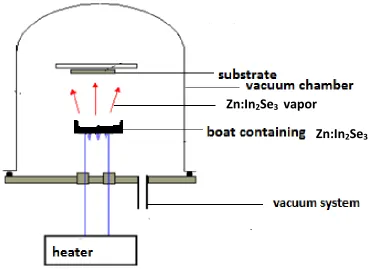
Figure 3.1: Schematic diagram of thermal evaporation system.
Zn:In
2Se
3vapor
Figure 3.1 shows a schematic diagram of thermal evaporation system. An electric
resistance heater is used to melt the material and raises its vapor pressure to a useful
vapor range. This is done in a high vacuum, both to allow the vapor to reach the
substrate without reacting with or scattering against other gas-phase atoms in the
chamber, and reduce the incorporation of impurities from the residual gas in the vacuum
chamber. Only materials with a much higher vapor pressure than the heating element can
be deposited without contamination of the film. Because the chamber is at a greatly
reduced pressure, there is a very long mean free path for the free atoms or molecules, and
the heavy vapor is able to reach the substrates placed at the top of the chamber. Here it
condenses back to the solid state, forming a thin, uniform film.
The evaporation rate is proportional to the difference between the equilibrium vapor
pressure of the liquid material and the vacuum pressure above it (Langmuir, 1916). The
mass evaporation rate per unit area in vacuum is given by Langmuir's equation:
5.834 x10⁻² (M /T) 1/2P (g / cm2) / s (3.1)
Where M is the molecular weight of the evaporating species (in g), T is the absolute
temperature of the liquid (in K), P is the equilibrium vapor pressure (in torr) of the liquid
metal at the temperature T. It is assumed that P is so much greater than the vacuum
3.2.2 Sputtering technique
Sputtering is a thin film deposition technique where atoms are dislodged from solid target
(source) surface and moves to the substrate through impact of gaseous ion mostly argon.
In this method atoms are dislodged from the surface of a target by high-energy particle
bombardment so that ejected atoms condense on a substrate as thin film. The atoms are
released from the source at a much lower temperature than in evaporation technique. The
source, also called the target, is put in a vacuum chamber and an inert gas is introduced at
low pressures. Gas plasma is then struck with an RF power source, ionizing the gas. The
ions are accelerated towards the target making atoms of the source material to break off
from the target in vapor form and condense on the substrate hence forming thin film.
The basic sputtering principle is similar for all sputtering technologies with the
difference being the manner in which the target is bombarded. Film thickness is
controlled by fixing the operating parameters and adjusting the deposition time. The
advantage of sputtering over evaporation is that it enables control of alloy composition
and other film properties such as step coverage and grain structure. However, this process
suffers from high capital expenses and low rate of deposition of some materials such as
silicon dioxide (SiO2). Organic solids are easily degraded by ionic bombardment and
therefore not used in this deposition process. The high capital expense is due to the fact
that sputtering process is energy intensive as it takes much longer time to deposit thin
Sputtering yield (number of atoms ejected per incident ion) is an important factor in
sputter deposition process since it affects the deposition rate. Three major factors that
affect the sputtering yield are target material, mass of bombarding particles and energy of
bombarding particles.
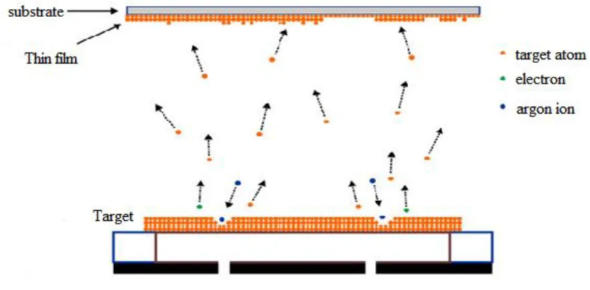
Figure 3.2 shows a schematic diagram of sputtering phenomenon. Energetic argon ions
from the plasma of gaseous discharge are attracted to the target (cathode) which they
bombard. Due to the bombardment of the target the atoms of the target together with
some electrons are ejected from the target surface. The target atoms are accelerated
towards the substrate (anode) where they are impinged to form a thin film coating. The
emitted electrons contribute in the production of more ions which sustains the discharge.
Sputter deposition may employ multiple targets making it possible to work with different
composition. Thin films processed using sputter deposition do not have good step
coverage (Burr et al., 2010). A minimum projectile kinetic energy needed to induce sputtering is called threshold energy (Eth) and is given by (Bohdansky,1984) ;
1 o th UE for 0.3
2 1
M M
(3.2)
where M1 is projectile mass, M2 is mean molecular mass per atom of a target and β is
maximum fractional energy transfer possible in a head-on collision given by:
22 1 2 1 4 M M M M
(3.3)
and for 0.3
2 1 M M , 3 1 2 1 0 8 M M U Eth (3.4)
Sputtering processes are wide and varied. There are four spattering arrangements; DC,
RF, magnetron and reactive. The arrangements employ almost similar mechanism of
atom ejection from the target. The arrangements are briefly discussed below.
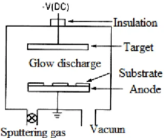
3.2.2.1 DC sputtering/RF sputtering
In DC sputtering the target is a plate material to be deposited or the material from which
thin film is synthesized. The target is placed at the cathode connected to the negative
terminal of the DC/RF supply. Several kilovolts are applied to the target. The substrate
that usually faces the target is either grounded, electrically floating, biased positively or
gas, typically argon is introduced into the chamber after evacuation. This serves as a
medium in which the discharge is initially sustained. The pressure of the gas usually
ranges from a few to 100 mtorr. After a visible glow, discharge is maintained between the
electrodes, it is observed that a current flows and a film condenses on the substrate
(anode). Microscopically positive ions in the discharge strike the cathode plate and eject a
neutral target atom through momentum transfer. These atoms enter and pass through the
discharge region to eventually deposit on the substrate. Regardless of the sputtering,
however, roughly similar discharge, electrode configurations and gas-solid interaction are
involved.
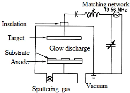
It is also worth noting that the DC and RF sputtering techniques follow similar
mechanisms except that RF sputtering has an additional matching network circuitry.
Figure 3.3 (b): Schematic diagram of RF sputtering set up (Ohring M, 1992)
3.2.2.2 Magnetron sputtering
In magnetron sputtering the superposition of electric and magnetic fields between the
substrate and the target yields a force on electron within the dual field environment. The
force is given by Lorentz equation described in equation 3.5;
F =md𝑣dt = −q(ε + 𝑣𝑋𝐵) (3.5)
Where q, m, 𝑣 are the electron charge, mass and velocity respectively.
By suitable orientation of the target magnets, a “race track” may be defined where the
electrons hope around at high speed. Target erosion by sputtering occurs within the track
because ionization of the working gas is most intense above it.
Magnetron sputtering takes the lead as the most widely used commercially practiced
(up to 1 𝜇𝑚/𝑚𝑖𝑛) which is higher than rates attained by conventional sputtering
techniques.
3.2.2.3 Reactive sputtering
Here thin films of compounds are deposited on the substrate by sputtering from metallic
targets in the presence of a reactive gas always mixed with the inert working gas such as
argon. Below are the most commonly reactively sputtered compounds;
a) Oxides (oxygen),
b) Nitrides (nitrogen and ammonium),
c) Carbides (methane, acetylene , propane),
d) Sulphides (H2S),
e) Oxycarbides and oxynitrides of Ti, Ta, Al and Si.
Irrespective of the material during reactive sputtering, the resulting films are either a solid
solution alloy of the target metal doped with element, compound or a mixture of the two.
3.3 Electrical resistivity in semiconductors
Unlike metals, semi-conductor materials are bipolar containing two charge carrying
particles of opposite sign. One carrier has a negative charge (free electron) of mobility
𝜇𝑛and the other has a positive charge (the hole), of mobility 𝜇𝑝 (Ohring, 1992). These
particles, when subjected to an electric field E, would move in opposite directions, but
𝐽𝑝𝑛 = (𝑛𝜇𝑛+ 𝑝𝜇𝑝)qE = σE (3.6)
where n is the concentration of free electrons, p is the concentration of holes, is the
conductivity and q is charge of the carrier.
Therefore,
σ = (n𝜇𝑛 + 𝑝 𝜇𝑝)q (3.7)
It is found from Fermi-function and density of states calculations that the number of
electrons per unit volume is given by;
𝑛 = 𝑁𝑐𝑒(𝜇−𝐸𝑔)/𝐾𝐵𝑇 (3.8)
While the number of holes per unit volume is
𝑝 = 𝑁𝑣𝑒−𝑢/𝐾𝐵𝑇 (3.9)
where Nc is effectivenumber of levels per unit volume in conduction band, 𝑁𝑣 the
effectivenumber of levels per unit volume in valence band 𝐾𝐵 represents Boltzmann
constant, 𝐸𝑔 band gap energy and is Chemical potential.
Combining equations of 3.8 and 3.9 we obtain;
𝑛𝑝 = 𝑁𝑐𝑁𝑣𝑒−𝐸𝑔/𝐾𝐵𝑇 (3.10)
The result is a function of temperature only and is independent of impurity concentration.
For a pure semi-conductor,
𝑛 = 𝑝 = (𝑁𝑐𝑁𝑣)1/2𝑒−𝐸𝑔/2𝐾𝐵𝑇
(3.11)
From equation (3.10) we know that σ = (n𝜇𝑛 + 𝑝 𝜇𝑝)q
Thus for a pure semiconductor σ becomes;
σ = 𝑝𝑞 (𝜇𝑛 + 𝜇𝑝) (3.12)
σ = (𝑁𝑐𝑁𝑣)1/2𝑞 (𝜇
𝑛 + 𝜇𝑝)𝑒−𝐸𝑔/2𝐾𝐵𝑇 (3.13)
this can also be expressed as;
σ = Ao𝑒−𝐸𝑔/2𝐾𝐵𝑇 (3.14)
In this case Ao= (𝑁𝑐𝑁𝑣)1/2𝑞 (𝜇𝑛 + 𝜇𝑝)
Therefore resistivity can be obtained by getting the reciprocal of equation (3.14) as
shown in equation (3.15).
𝜌 =1𝜎 =A1
o𝑒
𝐸𝑔/2𝐾𝐵𝑇
(3.15)
It follows therefore that ;
𝜌 = 𝐵𝑜𝑒𝐸𝑔/2𝐾𝐵𝑇 (3.16)
𝐵𝑜= 1
Ao= 1 ((𝑁⁄ 𝑐𝑁𝑣)1/2𝑞 (𝜇𝑛 + 𝜇𝑝)) (3.17)
Equations (3.14) indicate that the resistivity is inversely proportional to temperature for
semiconductors.
3.3.1 Thin film sheet resistivity
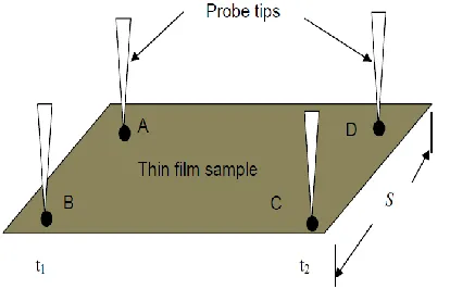
Figure 3.4 shows a sketch of four probes in square matrix for a four point probe.
In the case of a thin film (that is when the film thickness is much less than the probe
spacing), current rings instead of spheres are realized. The area (A) is therefore given as;
𝐴 = 2𝜋𝑥𝑡 where t is the film thickness (3.18)
From resistivity equation 𝑅 =𝜌𝐿𝐴 (3.19)
where R, 𝜌, 𝐿 and 𝐴 represent sheet resistance, resistivity, length and area respectively.
When length L is equated to the small change in x, dx, this small change and the value of A in equation 3.18 can be introduced into equation 3.19 and integrated between the
thicknesses t1 and t2 as indicated in equation 3.20.
𝑅 = ∫ 𝜌𝑡2 2𝜋𝑥𝑡𝑑𝑥
𝑡1 (3.20)
Considering the probe spacing (S) and integrating equation (3.20) becomes;
𝑅 = ∫ 𝜌𝑆2𝑆 2𝜋𝑥𝑡𝑑𝑥 (3.21)
𝑅 =2𝜋𝑡𝜌 𝐿𝑛2 (3.22)
Since 𝑅 = 2𝐼𝑉 due to current superposition, it can be shown that sheet resistivity (𝜌𝑠) of
thin films is given by;
𝜌𝑠 = 𝐿𝑛2𝜋𝑡 𝑉𝐼 (3.23)
It is noted that the sheet resistivity is independent of the probe spacing.
𝜌𝑠 = 4.532𝑡𝑉𝐼 (3.24)
It is reported that for a semi-infinite sheet K=4.53. However the factor will be different
for non ideal samples (James and Paul, 2002; Agwu et al., 2007).
The sheet resistance (𝑅𝑠) of a thin film is given by;
𝑅𝑠 =𝑙𝑛2𝜋 𝐹(𝑄)𝑉𝐷𝐶2𝐼+𝑉𝐵𝐶 Ω 𝑠𝑞𝑢𝑎𝑟𝑒⁄ (3.25)
where 𝑉𝐷𝐶2𝐼+𝑉𝐵𝐶 is the average resistance while F and Q are the symmetry and correction
factors respectively. F is a function of Q and is valid for Q less than 10. It is expressed in
the form;
𝐹 = 1 − 0.34657 [𝑄−1𝑄+1]2− 0.09236 [𝑄−1𝑄+1]4 (3.26)
The specific resistivity can be determined from the thin film thickness and the sheet
resistance in the form;
𝜌 = 𝑅𝑡10−1𝜇Ω𝑐𝑚 (3.27)
where t is the film thickness.
3.4 Phase Change Random Access Memory
3.4.1 Set /Reset Operations
Phase Change Random Access Memory, or PRAM, is a non-volatile memory that
exploits the unique behavior of phase change material to store information.The theory of
resistivity upon a change in phase in certain glasses (Ovshinsky, 1968).Phase change
material is widely used in rewritable CDs and DVDs, in which the same alloy is used as
the PCM memory developed by Numonyx (2008).By exploiting the electrical resistivity
of phase change material, PCM is drawing increasing interest recently, as it can be used
as a memory cell and organized into memory array similar to DRAM.
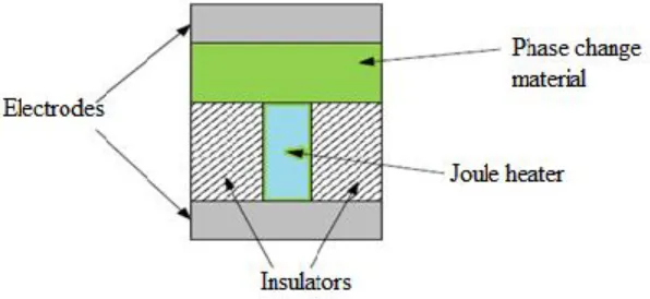
Figure 3.5: Simple structure of a PRAM cell (Ping , 2012)
Figure 3.5 illustrates the structure of a typical PRAM cell. A layer of phase change
material is sand-witched between two electrodes. A joule heater is placed between the
phase change material and the bottom electrode. The PCM forms the switching area of
the PRAM. The structure forms a PRAM cell, which appears as a resistance in the circuit.
Reading data from a PRAM cell involves sensing the resistance level of the cell. This is
done by applying a small voltage across the two electrodes so that the resistance of
PRAM can be measured. This process is non-destructive and has negligible heat stress
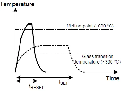
Figure 3.6: SET / RESET operations of a PRAM (Barclay, 2009)
Figure 3.6 represent the SET/RESET operation of a PRAM. A short pulse (tRESET) is used
to melt quench the phase change material to amorphous (high resistance) state. On the
other hand a longer pulse (tSET) is used to crystallize the PCM hence setting the cell to
low resistance (SET) state.
PRAM cell uses phase change material to remember a bit. The phase change material is
one type of 8 chalcogenide alloys, such as Ge2Sb2Te5 (GST), which has two stable
physical states: amorphous and crystalline. In the amorphous state, the material is highly
disordered and exhibits high resistivity. In the crystalline state, the material has a regular
crystalline structure and exhibits low resistivity. PRAM exploits the difference in
resistivity between these two states of the material to store data. Typically, a cell in the
amorphous state (high resistance) is regarded as a logic “0” (that is RESET state), and a
Basically in PRAM, the phase-change material is crystallized by heating it above its
crystallization temperature (SET operation), and it is melt-quenched to make the material
amorphous (RESET operation). These operations are controlled by electrical current.
High-power pulses for the RESET operation that places the memory cell into the
high-resistance RESET state, moderate power but longer duration pulses for the SET pulse
returning the cell to the low-resistance SET state, and finally very low power for
retrieving data by sensing the device resistance .(Raoux et al., 2008).
Unlike DRAM that relies on constant refresh to retain its data, the state of PCM is
preserved even after the cell is powered off, meaning that PRAM is non-volatile. PRAM
also has good data retention time (Bedeschi et al., 2008).
Fall time for a RESET pulse is a critical parameter. The state of the PCM technology
determines the required minimum for a fall time. Currently, it is a common requirement
to have 30-50 nanoseconds. New materials are expected to push that requirement to
shorter fall times. If the pulse fall time is longer than the required time, the material may
not effectively quench into an amorphous phase. Critical parameters for PCM device
characterization are re-crystallization rate, data retention, drift and read disturb. Current
re-crystallization rates are now as short as several tens of nanoseconds but they may soon
drop to as little as a few nanoseconds. The SET phase is a lower energy state and phase
change materials tend to re-crystallize spontaneously. The rate of crystallization is
temperature dependent. Therefore, data retention can be defined as a maximum
period. Data retention is typically 10 years. A measurement of how many times a
memory cell can be successfully programmed to the 0 and 1 states is called cycling
endurance. The new multi-state memory cells with additional distinct states mentioned
previously allow packing more memory into a single cell, which modifies cycling
endurance test procedures. Drift is simply a measure of the drift of the cell‘s resistance
over time. Read Disturb is an evaluation of how the read procedure impacts on the stored
state. The measurement pulse must be less than 0.5V. Higher voltages will lead to Read
Disturb problems.
3.4.2 Resistance-current (R-I) curves
The R-I curve is one of the most common parameters collected during PRAM
characterization. A pulse sequence is sent through a device under test, DUT. The first
pulse, a RESET pulse, sets the resistance of the DUT to the high value. It is followed by a
DC-read or MEASURE pulse that is usually 0.5V or lower in order to avoid affecting the
state of the DUT. This is followed by a SET pulse and another MEASURE pulse. The
entire sequence is repeated multiple times, with the amplitude of the SET pulse slowly
increased to the value of the RESET pulse. SET resistance values range from one
mega-ohm to several kilo-mega-ohms, depending on the value of the SET current.
3.4.3 I-V curves.
To generate the I-V curves, the starting point is a DUT that was previously RESET to its
The dynamic switch from a high- to-low resistive state in the presence of a load resistor
produces a characteristic R-I curve with a snapback, an area of negative resistance.
Snapback itself is not a feature of PRAMs or of PRAM testing, but rather a side effect of
the R-load technique that has long been used to obtain both R-I and I-V curves.
In the standard R-Load measurement technique a resistor is connected in series with the
DUT, allowing current to be measured across the DUT by measuring the voltage across
the load resistor. Active high impedance probes and an oscilloscope are used to record
the voltage across the load resistor. Current across the DUT is given by;
I
𝐷𝑈𝑇=
𝑉𝐴𝑃𝑃−𝑉𝐷𝑒𝑉𝑅𝐿𝑜𝑎𝑑 (3.28)
where I𝐷𝑈𝑇, 𝑉𝐴𝑃𝑃, 𝑉𝐷𝑒𝑉 and 𝑅𝐿𝑜𝑎𝑑 represent current across DUT, applied voltage,
developed voltage and load resistance respectively. The values of the load resistor usually
range from one to three kilo-ohms. This technique involves a tradeoff: if the load
resistance is too high, RC effects and the voltage division between the R-Load and the
DUT limits this techniques performance; however, if the resistor value is too small, it
impacts on the current resolution.
3.4.4 Reliability Considerations
PRAM cell reliability risks can be generically classified into three types: Data retention,
retain the data written into the cell over a prescribed period of time (and typically at a
maximum ambient temperature). Cycling endurance is the number of re-writes that can
be applied to the cell without failure. Data disturb is the ability to access a cell or
neighboring cells without un-intentionally changing the stored data. PRAM performs
well in each of these areas. It shows data retention capability to 10 years that is
independent of cycling whereas floating gate devices show a reduction in retention as
they are cycled. Cycling endurance is on the order of 108 writes, significantly higher than the ~105 specified for floating gate technologies (Gleixner et al., 2009). Finally, PRAM is robust to data disturbs. In addition to its ability to lithographically scale, these
characteristics make PRAM an attractive NVM for both traditional applications as well as
for applications that had previously been beyond the capability of floating gate devices.
At the cell level, the data retention and disturb risk of PRAM is primarily confined to the
RESET, or amorphous phase of the device. This results from the fact that the amorphous
state is meta-stable with respect to the stable crystalline phase. Any additional energy
applied to this state, via thermal or electrical energy, can accelerate the crystallization
process. For data retention, the energy is thermal and provided by the surrounding
ambient. There are two types of possible disturbs for the reset state. The first type, known
as proximity disturb, can occur in a RESET cell if surrounding cells are repeatedly
programmed. In this case, the heat generated during the programming operation diffuses
from the neighboring cells and accelerates crystallization. The other type of disturb called
Read disturb on the other hand, occurs when a device is read many times. This type of
3.5 Other Memory Technologies Currently In the Market
3.5.1 Static Random Access Memory (SRAM)
SRAM is non volatile meaning it cannot holds data when the power is OFF. It is referred
to as static in the sense it does not require constant refreshing, meaning that as long as the
power is applied the data written on it remains static. This memory has three operation
states, that is, hold, write and read. These states depend on the status of the word line.
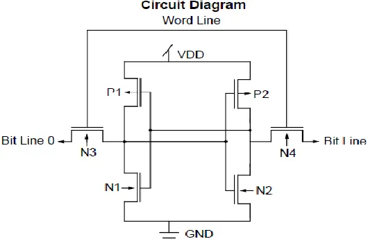
Figure 3.7 shows an SRAM cell consisting of six MOSFET switches P1, P2, N1, N2, N3
and N4 four of which are cross-coupled inverters. The reading operation is carried out by
pre-charging both Bit line 1 and Bit line 0 to logic 1 and then asserting the Word Line.
On the other hand the writing operation is achieved by giving the desired logic status to
the Bit Line 1 and its complement Bit line 0 and then asserting the Word line.
An SRAM memory cell is a bi-stable flop made up of four to six transistors. The
flip-flop may be in either of two states that can be interpreted by the support circuitry to be a
1 or a 0. The current SRAM cells are made of six transistors unlike previously when they
used to have four transistors. The use of six transistors was hutched due to the numerous
draw backs of the four transistor cells including; high leakage current which results into
high standby current as well as vulnerability to radio-induced soft errors. Six transistor
cells are on the other hand highly stable, relatively impervious to software errors and
have relatively low leakage and standby current. SRAM memory arrays are arranged in
rows and columns of memory cells called word lines and bit lines, respectively. In IBM
SRAMs, the word lines are made from poly-silicon while the bit lines are metal. Each
memory cell has a unique location or address defined by the intersection of a row and
column. Each address is linked to a particular data input/output pin. The number of arrays
on a memory chip is determined by the total size of the memory, the speed at which the
memory must operate, the layout, testing requirements and the number of data I/Os on the
chip. The main advantages of SRAM over DRAM are the speed and the ability to hold
data as long as the power is supplied without continuous refreshment.
Most SRAM cells are used in computers where it is embedded close to the central
processing unit (CPU) and it functions as a high performance cache memory. This
embedded cell runs at CPU clock speed with access time of less than ten nanoseconds.
SRAM in combination with NOR flash is used in cell phones where it runs at slower
clock speeds allowing clock speeds of nanoseconds. SRAM has infinite read/write
3.5.2 Dynamic Random Access Memory (DRAM)
DRAM is referred to as dynamic RAM simply because it requires constant refreshing to
maintain the data written on it. This therefore means that without periodic rewriting this
memory may lose data even when the power is not interrupted. This memory is a volatile
memory meaning that it maintains the data as long as the power is supplied.
Dynamic random access memory (DRAM) serves as the main memory of personal
desktop computers, laptops, gaming consoles, and high-end phones. A DRAM cell
consists of a single transistor and single capacitor, allowing great density in the order of
several Gb per chip (Samsung, 2009). DRAM is a volatile memory technology, meaning
that it requires routine refreshing of its data every few milliseconds, although some of its
stored data may still be recoverable after several seconds, depending on environmental
parameters (Halderman et al., 2008). Its high density makes it less expensive per bit as compared to SRAM. However due to its periodic refreshment it requires more peripheral
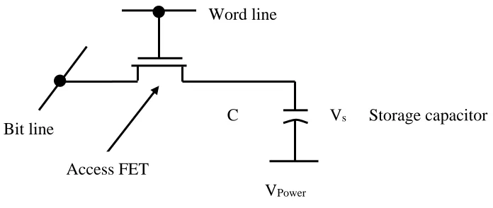
circuitry as compared to the SRAM. Figure 3.8 shows a schematic diagram of a DRAM
consisting of a capacitor Cs and a FET. The capacitor is used to store each bit of data
whereas the FET is used as a switch or an access transistor. The level of charge on the
capacitor determines whether the bit stored is logic “1” or logic “0”. The presence of
charge in the capacitor indicates logic “1” while the absence of charge in the capacitor
indicates logic “0”. DRAM is used in more set of applications as compared to SRAM. It
has access times of tens of nanoseconds for computer and other consumer applications.
For embedded DRAM used in video RAM and cache memory access time of ten
Figure 3.8: Schematic Diagram of a DRAM Cell (Zilberberg et al., 2013)
Write endurance can be estimated using the following equation;
𝐸 = 𝑇𝐿𝑖𝑓𝑒 𝐵
𝛼𝐶 (3.29)
Where E is endurance, Tlife is life expectancy of the system, B is memory bandwidth, α is
wear-leveling efficiency and C is the system memory capacity
Table 3.1: Basic attributes of emerging memory technology (Ping, 2012)
Read speed Write speed Cell area Endurance Byte-addressable
DRAM 20-50ns 20-50ns 6𝐹2 1015 Yes
SRAM ∽ 2𝑛𝑠 ∽ 2𝑛𝑠 146𝐹2 1015
− 1016 Yes
NAND Flash
25𝜇𝑠 500𝜇𝑠 5𝐹2 104− 105 No
STT-RAM ∽ 2𝑛𝑠 ∽ 10𝑛𝑠 37 − 40𝐹2 1012 Yes
PCM 30-50ns ∽ 1𝜇𝑠 5 − 8𝐹2 ∽ 108 Yes
Vs Storage capacitor C
s
VPower Access FET
Word line
As the technology enters the nanoscale regime, large DRAM-based main memory faces
serious leakage and scalability limitations. Lefurgy et al., 2003 reported that in the mid range, IBM e-Server machine, about 40% of the power was consumed by the main
memory. DRAM memory is also facing serious problems scaling to 40 nm or below, as it
is constrained by the limitation in cell-bit line capacitance ratio. As a result, people have
resorted to several non-volatile memory technologies as alternatives to conventional
DRAM. Examples include NAND Flash, Phase Change Memory (PCM) and
Spin-Transfer Torque RAM (STT-RAM). Although DRAM lags behind NAND flash and
standard CMOS logic technologies in terms of scaling to 45 nm technology node and
preparation for 32 nm node, it is a very reliable technology used in modern computers.
3.5.3 Flash Memory
Flash memory is a nonvolatile memory technology whose cells use floating gate devices.
Flash is organized in two variations; NOR flash, which is not very dense, and therefore is
used mainly for code storage, for example, as boot up software. The other form is NAND
flash, which is commonly used as data storage in mobile devices, such as digital cameras
and digital audio players and is also becoming widely used in laptop computers. Being
nonvolatile, it requires no power to maintain the data stored in it, unlike DRAM.
Moreover, NAND flash has faster access times and more shock resistance than magnetic
disks (HDDs). It is also considered more durable and can sustain higher pressures. Its
main limitations are the need to erase whole blocks of it (resetting the cell’s values to 0),
which forces the memory controller to rewrite some of the data after it has been erased,
Typically, flash devices can withstand about 1,000– 10,000 program-erase cycles
(MicronFlash, 2008). It should be noted that the number of program-erase cycles is not an
accurate criteria for flash endurance, since flash is typically written iteratively, and its
value is checked after several such cycles. Should the value be incorrect after a certain
threshold, the operation is deemed as a failure. But by increasing this threshold, it is
possible to increase the number of program-erase cycles supported, at the expense of
write operation latency.
3.5.3.1 NOR Flash
The NOR architecture is currently the most popular flash architecture commonly used in
EPROM and EEPROM designs. Aside from active transistors, the largest contributor to
area in the cell array is the metal to diffusion contacts. NOR architecture requires one
contact per two cells, which consumes the most area of all the flash architecture
alternatives. Electron trapping in the floating gate is done by hot-electron injection.
Electrons are removed by Fowler-Nordheim tunneling. The world’s leading
manufacturers of flash devices (Intel, AMD) use NOR cell configurations. Figure 3.9
shows a schematic diagram of a NOR flash. The cells of a NOR flash are arranged in
parallel. The read voltage to the control gate is therefore the same in all the cells. A
written cell sinks current much more than an erased cell. The written cell is logic “0”
Figure 3.9: Schematic diagram of a NOR Flash architecture (Elnec, 2008)
Some of the outstanding properties of the NOR flash include;
Capacity of about 1Gb
Random access method
Full memory interface
Fast read (random Access)
Slow Write and erase (about 1s/block)
Life span of about 10000-100000 write /erase cycles
Relatively high price
3.5.3.2 NAND Flash
NAND Flash is a high-density, low power, cost effective, and scalable design. It is an
ideal choice to fuel the explosion of new multimedia products that are entering the
market. Advances in system design techniques also enable the more cost effective NAND
Flash to replace NOR Flash in a significant percentage of traditionally NOR Flash
Due to the efficient architecture of the NAND Flash, its cell size is almost half the size of
a NOR cell. This enables NAND Flash architecture to offer higher densities with larger
capacity on a given die size, in combination with a simpler production process. The
NAND architecture is more cost-effective for higher capacities than the NOR
architecture. As mentioned above, the NAND Flash memories are ideal for data storage,
for instance, in MP3 players or digital cameras
Physically, the NAND architecture uses smaller transistors, because it doesn't have to
“pull-down” a whole bit-line. A NAND bit line is a series of transistors so each transistor
only has to pass a small amount of current. Figure 3.10 shows, how the transistors are
connected for NAND architecture. In this architecture, the transistors are connected in
series in groups of 16 or 32. Two selection transistors are placed one at the edge of the
stuck and the other at the bit line to ensure connection to the ground and to the bit line
respectively. when the cell is read its gate is set to 0 V while the other gates of the stuck
are biased with higher voltages between 4-5V. A programmed NAND flash cell has a
positive threshold voltage while an erased cell has a negative threshold voltage.
Some outstanding properties of NAND flash are listed below
Capacity of about 32Gb
Sequential access method
I/O interface
Fast read (serial access)
Fast write and erase (approximately 2ms/block)
Life span off about 100000-1000000
Relatively low price
Besides PCM and Flash, there are other alternative memory technologies considered for
solid-state memories. Two such leading technologies are FeRAM and MRAM, though
PCM has been demonstrated to be feasible with smaller device dimensions than these
technologies (Burr et al., 2010).
3.5.4 Ferroelectric Random Access Memory (FeRAM)
FeRAM, is a RAM with a similar construction to DRAM. However, FeRAM substitutes
DRAM’s dielectric layer with a ferroelectric layer. This causes the FeRAM to be a
nonvolatile memory. FeRAM was first proposed in the 1950s but has been developed
mainly by Ramtron in the mid 2000s. Small scale FeRAM is now commercially available
and has been used instead of NOR flashes in some chips. FeRAM has been suggested for
3.5.5 Magnetoresistive Random Access Memory (MRAM)
MRAM is a nonvolatile memory technology that does not use electric charge to store
data, but instead uses magnetic properties (Huai, 2008). It consists of two ferromagnetic
plates and an insulating layer. One layer has a constant polarity, while the other can be
switched between polarities, effectively storing a data bit. A 32Mbit RAM device has
been demonstrated, and smaller 4Mbit devices have been marketed. MRAM has also
CHAPTER FOUR
EXPERIMENTAL PROCEDURE
4.1 Introduction
This chapter discusses the methods of preparing the sample, formation of the alloy as
well as the thin film deposition by employing sputtering/ evaporation method. The
chapter also discusses the electrical characterization of thin films, PRAM fabrication and
its electrical characterization. The use of four point probe system for sheet resistance
determination for the during thermal cycling is explored.
4.2 Zn:In2Se3 alloys synthesis and thin film deposition
Elements of In and Se granules, of purity 99.999% were synthesized in the ratios of In:Se
of 2:3 by mass. Zn of similar purity was then introduced into the sample at a range of
ratios (0%, 2%, 4%, 6% and 8%) by mass. The composition was then loaded in Pyrex glass
tube and then sealed before heating in the presence of argon flow. The temperature was
controlled to range between 450 oC to 500 oC. During heating there was slight shaking of the tube to obtain homogeneity. The obtained homogenous solid alloy was ground in a
porcelain motor. For each composition four sets of samples were prepared for testing
The Edward Auto 306 RF/DC magnetron sputtering / evaporation chamber was first
vacuum-cleaned to remove dust debris before the ground Zn doped alloys were separately
(one sample at a time) placed in the evaporating boat. Thoroughly cleaned microscope
glass slides measuring 38 mm by 26 mm and 1 mm thick were used as substrates and
mounted on the chambers substrate holder. The chamber pressure was then pumped down
to 3.0 x 10⁻⁵ mbar pressure at room temperature. The Edward Auto 306 RF/DC magnetron
system was switched on to allow the alloy to evaporate and deposit uniformly on the
glass substrate to form a thin film.
Figure 4.1 shows the set up for the Zn:In2Se3 alloy formation. Argon gas from the gas
cylinder was allowed to flow as the sample in the sealed glass tube was heated. The argon
flow was aimed at eliminating the chances of oxidation. The temperature of the sample
was closely monitored using the digital thermometer. After melting, the alloy was
allowed to cool in the presence of argon.