A
BSTRACTPREBLE, EDWARD ALFRED. Structural and Microstructural Characterization of III-Nitrides on 6H-SiC (0001) Substrates. (Under the direction of Robert F. Davis)
Characterization of nitride films on 6H-SiC (0001) wafers via x-ray, TEM, and AFM was accomplished on standard GaN thin films with AlN or AlGaN buffer layers. TEM sample thinning capability was improved through the use of Nomarski in an optical microscope to gauge the thickness of the sample during preparation. TEM analysis was then completed of Au and Pt films deposited on chemical vapor cleaned GaN with annealed up to 800°C. Chemical reactions were detected in x-ray measurements of the 800°C Pt samples and GaN/metal interface roughening were confirmed by TEM images in both metals. Interface roughening is attributed to the chemical reactions and interfacial stresses greater than the yield stress of the metal created during heat treatments by the difference in the thermal expansion coefficients of the GaN and the metals.
The GaN rocking curves were found to track very closely to the values of the underlying substrate and changes in buffer layer growth temperatures were found to change the screw and edge dislocation populations of subsequent GaN layers. GaN grown on 1030°C AlN buffer layers showed the lowest edge dislocation populations when compared against buffers grown in the range of 1010-1220°C, even though the 1220°C AlN was much smoother. AlGaN buffer layers provided more edge dislocation reduction, with a 1090°C Al0.2Ga0.8N layer yielding the best GaN rocking curve values
GaN films with AlN buffer layers grown on hydrogen etched SiC substrates did not show rocking curve improvement when compared against samples with unetched substrates. The AlN layers showed extremely narrow, substrate limited, on-axis rocking curve values, but it is not clear as to whether additional defects are present that may broaden the off-axis rocking curves, causing the poorer results seen in the GaN films.
STRUCTURAL AND MICROSTRUCTURAL
CHARACTERIZATION OF III-NITRIDES
ON 6H-SiC (0001) SUBSTRATES
by
EDWARD A. PREBLE
A dissertation submitted to the Graduate Faculty of North Carolina State University
in partial fulfillment of the requirements for the Degree of
Doctor of Philosophy
DEPARTMENT OF MATERIALS SCIENCE AND ENGINEERING
Raleigh
2001
APPROVED BY:
_________________________________ _______________________________ Dr. Zlatko Sitar Dr. John Hren
_________________________________ _______________________________ Dr. Robert F. Davis Dr. Mohamed Bourham
B
IOGRAPHYEdward Alfred Preble was born in Hamilton, Ontario, on August 11, 1971, to Donna and Forrest Preble. He spent his early years living with his parents and grandparents in Summerside, Prince Edward Island, and then moved to Massachusetts before beginning pre-school. The majority of Edward's upbringing and education was completed in Walpole, Massachusetts, which is a suburb of Boston.
After Edward graduated from Walpole High School in 1989, he moved to Worcester, Massachusetts to attend Worcester Polytechnic Institute (WPI) and pursue a degree in mechanical engineering. Graduation from WPI in December 1993 brought Edward to North Carolina State University (NCSU) for graduate studies in nuclear engineering, with a focus on nuclear materials. In 1996, he obtained his Master of Science degree under the direction of Dr. K.L. Murty and through research oriented internships at two General Electric facilities, one in Wilmington, North Carolina and the other in Pleasanton, California. During his Master's degree work, Edward met his future wife, Wendy Taylor, who is also 1996 NCSU engineering graduate.
A
CKNOWLEDGEMENTSThe acknowledgments in a PhD thesis are what many consider to be the most important part of the thesis from a personal perspective. It would be impossible to complete a large study, such as this one, without the support of people like those that I mentioned below. This is because scientific research in academic environments rarely proceeds without trials of character. Equipment difficulties and theoretical puzzles are weekly occurrences, which, with the support of family, friends, and colleagues become tolerable and surmountable. In fact, their support furthered my ability to push forward to new accomplishments, and the end results are as much theirs, as they are mine.
I would first like to extend thanks to my wife, Wendy, along with my parents, Donna and Forrest, and my sister, Julie, who provided me with all of the support that I could ever need. My academic accomplishments are a direct reflection of the support, example, and encouragement they have given me throughout my entire life. In fact, Wendy should probably be listed as co-author for everything that I’ve done as she has listened to, and helped focus, all of my ideas over the many years I’ve known her. If you’ve ever had the opportunity to listen to an engineer speak about their work, you’ll know that if you aren’t involved with the work directly, the discussion can be less than exciting. Wendy helped out anyway, completing a harder job than I.
accomplished more in that team than would have been possible alone. I’d also like to thank many others in the Davis research group, including Dr. Kieran Tracy, Dr. Eric Carlson, Dr. Drew Hanser, Dr. Sven Einfeldt, Zach Reitmeier, Phil Hartlieb, Andrew Banks, and Darren Thomson. In addition, Jan Jackson and Edna Deas helped out on so many occasions, with so many problems, that it’s impossible to even consider listing them all. Finally, my advisor, Dr. Robert Davis provided the entire environment for our collective success here at NCSU. His patience, guidance, and interest in all of the many subjects that were investigated are irreplaceable. This thesis, and all of the research presented in it, was made possible because of the group that Dr. Davis has assembled and guided with all of his energy.
I’ve also had the benefit of several collaborations outside of NCSU with industry and academic colleagues. Dr. Martin Albrecht, at the University of Erlangen, Germany, was a gracious host and teacher for four trips to Germany. Dr. David Smith at Arizona State University, and Dr. Pirouz Pirouz, at Case Western Reserve University, opened their laboratories and resources to me very generously. In addition, Dr. William Vetter and Dr. Michael Dudley at the State University of New York at Stony Brook ran several experiments on their own time to help me verify and complete a large portion of my studies.
T
ABLE OFC
ONTENTSList of Figures... ix
List of Tables... xii
1. Introduction... 1
1.1 GaN Background ... 1
1.2 References... 6
2. X-ray characterization of AlN and GaN thin films grown on H-etched 6H-SiC substrates... 8
Abstract ... 9
2.1 Introduction... 10
2.2 Experimental Details... 10
2.3 Results... 11
2.4 Conclusions... 12
2.5 References... 14
Figures... 15
3. Removal of 6H-SiC substrate influence when evaluating GaN thin film properties via x-ray... 17
Abstract ... 18
3.1 Introduction... 19
3.2 Experimental Details... 20
3.3 Results... 22
3.3.1 6H-SiC Variability ... 22
3.3.2 GaN Epitaxial Thin Films on 6H-SiC... 22
3.3.3 Rocking Curve Improvement with Increased Thickness ... 25
3.3.4 Buffer Layer Effects on GaN Dislocation Populations... 26
3.3.4.1 AlN Buffer Layers ... 27
3.3.4.2 AlGaN Buffer Layers... 27
3.4 Conclusions... 28
3.5 References... 29
4. Application of Nomarski interference contrast microscopy as a thickness monitor in the preparation of transparent, SiC-based, cross-sectional TEM
samples ... 39
Abstract ... 40
4.1 Introduction... 41
4.2 Interference Contrast Theory ... 42
4.3 Experimental Details... 44
4.3.1 Materials and Equipment ... 44
4.3.2 Cross-Sectional TEM Specimen Preparation and Observation ... 45
4.4 Application of Interference Contrast for Thickness Determination ... 47
4.4.1 GaN/AlN/6H-SiC(0001) Structures... 47
4.4.2 Metal/Thin Film Heterostructure/Substrate Assembly ... 48
4.5 Acknowledgements... 49
4.6 References... 50
Figures... 51
5. Correlation of the electrical properties and the structural and microstructural characteristics of deposited and annealed Pt and Au contacts on chemical-vapor-cleaned GaN thin films ... 55
Abstract ... 56
5.1 Introduction... 57
5.2 Experimental Details... 57
5.3 Results... 60
5.3.1 As-Deposited Contacts... 60
5.3.2 Annealed Contacts ... 60
5.4 Conclusions... 63
5.5 Acknowledgements... 64
5.6 References... 65
Tables ... 66
Figures... 67
6. Crystallographic tilt and strain in uncoalesced, maskless pendeo-epitaxy GaN stripes ... 72
Abstract ... 73
6.1 Introduction... 74
6.3 Results... 76
6.4 Conclusions... 78
6.5 References... 79
Figures... 80
7. Summary... 82
7.1 Summary of Hydrogen Etching of SiC Substrates ... 82
7.2 Summary of SiC Substrate Variation... 83
7.3 Summary of SiC TEM Sample Preparation... 84
7.4 Summary of Au and Pt Contacts on GaN ... 84
7.5 Summary of Tilt in Pendeo Wings... 85
8. Proposed Future Research ... 86
8.1 Hydrogen etching of SiC substrates... 86
8.2 SiC/GaN X-ray Correlation ... 86
8.3 Nomarski as a tool for SiC cross-sectional TEM samples... 87
8.4 TEM of Contacts on Cleaned GaN ... 88
8.5 Wing Tilt of Pendeo Samples ... 88
A1. X-ray Rocking Curve Mapping of Wafers ... 90
A1.1 Goal of Mapping Technique ... 90
A1.2 Mapping Procedure ... 91
A1.3 Typical Rocking Curves of SiC ... 92
A1.4 Map of SiC Wafers ... 93
A1.5 Repeatability ... 94
A1.6 Validation of the Procedure ... 95
A2. Visual Basic Codes for Importation and Analysis of Wafer Map Data... 97
A2.1 Purpose of Codes ... 98
A2.2 Program Usage... 98
A2.2.1 Overview... 98
A2.2.2 Data Importation ... 100
A2.2.3 Results... 102
A2.3 Visual Basic Code Listing... 102
A3. Cross-Sectional TEM Specimen Preparation In Detail... 115
A4. Visual Basic Codes for the Importation and Analysis of Reciprocal
Space Map Data ... 121
A4.1 Purpose of Codes ... 122
A4.2 Program Usage... 122
A4.2.1 Overview... 122
A4.2.2 Data Importation ... 122
A4.2.3 Calculating the Angles, S-Space, and Q-Space Values ... 123
L
IST OFF
IGURESFigure 2-1 – AlN rocking curves for as-received and H-etched high-doped 6H-SiC ... 15
Figure 2-2 – AlN FWHM vs. SiC FWHM for As-received and H-etched samples. ... 15
Figure 2-3 – On-Axis GaN FWHM vs. SiC FWHM ... 16
Figure 2-4 – Off-Axis GaN FWHM vs. SiC FWHM ... 16
Figure 3-1 – Histogram of 6H-SiC (00.6) Full-Width Half-Maxima (FWHM) obtained to date ...30
Figure 3-2 – SiC (00.6) FWHM map showing domain variations in arc-seconds on a typical wafer... 31
Figure 3-3 – (00.6) FWHM maps from a single boule. Note the strong special correlation of the high and low FWHM regions in each of the wafers... 32
Figure 3-4 – Several GaN (00.2) rocking curves mimicking the underlying SiC (00.6) rocking curves ... 33
Figure 3-5 – GaN (00.2) FWHM vs. SiC (00.6) FWHM. The SiC wafer increases the GaN rocking curve FWHM values in a 1:1 fashion above a critical value (~200”). ... 34
Figure 3-6 – Off-axis GaN (10.3) FWHM vs SiC (10.9) FWHM. The higher FWHM of the off-axis GaN peak does not reach the SiC threshold until ~350”. The higher the GaN FWHM value, the less it is adversely effected by the SiC wafer. ... 35
Figure 3-7 – GaN edge dislocation estimation via inclination angle plot as a function of thickness of the GaN film... 36
Figure 3-8 – SEM of 1010°C (left), 1130°C (center), and 1220°C (right) AlN surfaces . 36 Figure 3-9 – GaN edge dislocation estimation via inclination angle plot as a function of AlN buffer layer growth temperature ... 37
Figure 4-1 – (a) Newton's Fringes, as theorized by Newton[5] and (b) a modern day photo of Newton’s fringes created by a curved lens on top of a glass sheet.[6]... 51 Figure 4-2 – Reflection and refraction in a thin transparent wedge. ... 51 Figure 4-3 – Effect of sample rotation on the intensity of the interference fringes. The
exposure of photo (a) was 0.002 seconds, while the exposure of photo (b) was 0.25 seconds (125 times longer). Note the repeating red/green pattern of the larger (thicker material) rings in photo (a), which progress to a rainbow pattern as the sample thins. The white material is <1µm thick... 52 Figure 4-4 – Optical and SEM images of a dimpled sample. The optical image (a)
shows the Nomarski top view of one SiC piece. The dark line in the center of image (a) is the edge of the copper support ring, seen under the thicker, left side of the sample. The SEM images (b) and (c), are side views of the areas indicated. ... 52 Figure 4-5 – Thickness measurements of SiC correlated to Nomarski fringes ... 53 Figure 4-6 – The computer enhanced inset in this image shows secondary interference
fringes in electron transparent SiC. The top right corner of the enhancement is a hole, and the location of the enhancement was not changed with respect to the rest of the image. ... 53 Figure 4-7 – HRTEM of a Gold/GaN interface. The GaN was grown on a SiC
substrate that was prepared for TEM using the technique described in this paper. ... 54
Figure 5-1 – Plot of the ratios of intensity (area) of the XPS Ga core levels of the sequentially deposited Pt and Au films (Is)/ the intensity of the uncoated sample (Io) as a function of film thickness. ... 67 Figure 5-2 – Scanning electron micrographs of the as-deposited surfaces of ... 67 Figure 5-3 – Cross-sectional transmission electron micrographs of the interfaces of
as-deposited Pt/GaN (left) and Au/GaN. ... 68 Figure 5-4 – Current-Voltage curves for the as-deposited and the annealed Pt (top),
and Au contacts... 69 Figure 5-5 – Scanning electron micrographs of the surfaces of the Pt (left) and Au
Figure 5-6 – Cross-sectional electron micrographs of the Pt/GaN (left) and the
Au/GaN interface after annealing for 3 minutes at 800°C... 70
Figure 5-7 – X-ray diffraction spectra showing 2Q/w profiles for the Pt (top) and Au contacts. Different temperatures are offset for ease of viewing. All data is normalized to the SiC (0006) peak... 71
Figure 6-1 – SEM images and (002) reciprocal space maps of small wing sample. When the incident x-ray beam is perpendicular to the stripes, the tilt in the wings is resolvable. When the x-ray incidence direction is parallel to the stripes the wing and seed layer peaks overlap and are not resolved. ... 80
Figure 6-2 – SEM images and (002) reciprocal space maps of large wing sample... 81
Figure A1-1 - X-ray map sampling matrix with respect to a 2-inch SiC wafer... 91
Figure A1-2 - Rocking curve of a good region of SiC ... 92
Figure A1-3 - Rocking curve of a poor region of SiC ... 93
Figure A1-4 - Typical X-ray map of a wafer ... 94
Figure A1-5 - Si (111) standard wafer map showing little variation. ... 96
Figure A2-1 - Data Importation Page of Template Program ... 99
Figure A2-2 - Results Page of Template Program... 100
Figure A2-3 - Array example matrix showing typical scan points of a 2" wafer ... 101
Figure A3-1 - Sandwich slicing and stacking schematic ... 119
L
IST OFT
ABLESTable 5-1 – Calculated stress and strain values of Pt and Au contacts on GaN during annealing ... 66
1.
INTRODUCTION
1.1 GaN Background
Gallium nitride, a semiconductor with a direct bandgap of 3.4eV, has considerable realized and future potential for optoelectronic and microelectronic applications. It is currently used in the manufacture of blue and green light-emitting diodes and blue emitting laser diodes. Considerable research is being conducted to achieve improved high frequency and/or microelectronic devices based on GaN due to its thermal stability and large direct energy gap.[1-3] Metallorganic vapor phase epitaxy (MOVPE) and molecular beam epitaxy (MBE) are the primary methods for the epitaxial growth of GaN device structures on sapphire and silicon carbide based substrates. The use of foreign substrates, which are not closely matched to GaN in terms of atom-atom separation and coefficients of thermal expansion, results in the introduction of residual stresses into the growing films. These stresses are subsequently and partially relieved by the formation of misfit and threading dislocations with a density of 108-1010 cm-2,[4-7] that lead to deterioration in the electrical and optical character of devices produced using the III-nitrides.[8-11]
hydrogen etching. This approach removes polishing scratches and subsurface damage as well as produces atomically flat terraces that are typically several thousand angstroms wide and separated by unit cell high steps. This etched surface is seen as advantageous for the sequential heteroepitaxial growth of AlN buffer layers and GaN films, because the step height of the 6H-SiC allows the nucleation and growth of the 2H polytype of these nitrides without the formation of stacking mismatch boundaries normally caused by the misregistry in the atomic stacking of two adjacent crystal structures.[20] We have both capitalized and built upon this knowledge base regarding etching and growth on the etched SiC(0001) surface with the development and employment of our own SiC etching capabilities, the characterization of the substrates before and after etching and the determination of the character of the AlN and GaN films grown on these substrates.
Unfortunately, 6H-SiC boules are created through a process that yields crystals containing subgrains of the cubic 3C polytype, numerous filled and open screw dislocations and micropipes, and also low-angle subdomain boundaries in the 6H polytype structure. These imperfections propagate into the III-Nitride epitaxial films grown on the surface and affect the structural and microstructural character as well as the physical properties of these films to the extent that the substrate variability cannot be ignored. Indeed, substrate variability causes changes in the x-ray rocking curves of the nitride films that are sufficiently large to hide changes of the film properties due to differences in thickness or buffer layer parameters.
on the substructure and microstructure of the epitaxial AlN and GaN films grown upon them. Moreover, a method has been determined and used to account for the influence of the substrate domains when comparing the rocking curve data of the AlN and GaN films. In other words, this method provides information regarding the structural character of the films, without the influence of substrate variations. These studies and the results and conclusions derived from them are detailed in Chapter 2. Additional details and applications of this new method as well an expansion of the study to include investigations regarding the effects of thickness and growth temperature and the resulting porosity of the AlN buffer layer on the substructure and microstructure of GaN films grown on the AlN/SiC substrates is presented in Chapter 3.
The understanding of the domain and defect substructures of the SiC substrate and their influence on the subsequently grown epitaxial films requires both the sophisticated X-ray studies noted above as well as a visual determination of the location and densities of these entities as provided by transmission electron microscopy (TEM). Due to the transparent nature of SiC, the preparation of extremely thin TEM samples is difficult using traditional methods that depend on the sample being opaque until very thin. Chapter 4 of the thesis discusses the use of Nomarski differential interference contrast as a thickness monitor during the preparation of SiC-based TEM samples. Experimental details as well as theoretical information are presented.
variability. Moreover, physical and chemical degradation of these contacts employed in devices based on the III-Nitrides are likely to occur under their anticipated operating conditions.[21] Some of this variability can be attributed to differences in surface preparation prior to contact deposition.[22] The discussion presented in Chapter 5 correlates the electrical data obtained from the Schottky contacts on chemical vapor cleaned GaN with structural data obtained via high-resolution TEM, high-resolution x-ray diffraction, and scanning electron microscopy of the film surfaces. Degradation of the contact performance is also tied to structural and chemical changes observed in the aforementioned techniques.
Other recent research in the Davis laboratories has focused on the growth of material through selective growth techniques such as lateral epitaxial overgrowth (LEO)[23,24] and pendeo epitaxy (PE)[25] that can be utilized to grow material that is shielded from the propagation of threading defects through lateral growth. Dislocation populations have been reduced by several orders of magnitude in the laterally grown regions. Additionally, devices such as laser diodes that are placed on the lower defect regions exhibit superior operating behavior.[26]
Pendeo-epitaxy (PE) involves lateral growth of film material (wings) from the sides of a seed crystal. Recent X-ray and selected area diffraction studies have shown that the wings are tilted with respect to the adjacent striped seed regions from which they grew. Coalescence of these tilted crystal planes form tilt boundaries, which if large enough, could cause degradation in devices fabricated over these regions.
from that of the seed material in samples that have not coalesced. The wing regions show strain reduction and rocking curve improvements when compared against the seed materials. Additionally, the wing material is shielded from the effects of a poor substrate. The tilt values that are found in the pendeo wings are among the lowest observed in selected area growth samples reported to date.
1.2 References
1. S. Nakamura, T. Mukai, M. Senoh, Appl. Phys. Lett. 64, 1687(1994)
2. S. Nakamura, M. Senoh, S. Nagahama, N. Iwasa, T. Yamada, T. Marsushita, H. Kiyoku, Y. Sugimoto, Jpn. J. Appl. Phys., 35, L74(1996)
3. S. Nakamura, J. Cryst. Growth, 170, 11(1997)
4. F.A. Ponce, J.S. Major, Jr., W.E. Plano, and D.F. Welch, Appl. Phys. Lett. 65, 2303 (1994).
5. F.A. Ponce, B.S. Krusor, J.S. Major, Jr., W.E. Plano, and D.F. Welch, Appl. Phys. Lett. 67 (3), 1995.
6. F.R. Chien, X.J. Ning, S. Stemmer, P. Pirouz, M.D. Bremser, and R.F. Davis, Appl. Phys. Lett. 68 (19), 1996.
7. W. Qian, M. Skowronski, M. Degraef, K. Doverspike, L.B. Rowland, and D.K. Gaskill, Appl. Phys. Lett. 66, 1208 (1995).
8. S. Keller, B.P. Keller, Y.-F. Wu, B. Heying, D. Kapolnek, J.S. Speck, U.K. Mishra, and S.P. DenBaars, Appl. Phys. Lett. 68, 1525 (1996).
9. N. Kuroda, C. Sasaoka, A. Kimura, A. Usui, and Y. Mochizuki, Proceedings of the Second Annual International Conference On Nitride Semiconductors, 392, (1997). 10. S. Nakamura, M Senoh, S. Nagahama, N. Isawa, T. Yamada, T. Matsushita, H. Kiyoku, Y. Sugimoto, T. Kozaki, H. Umemoto, M. Sano, and J. Chocho, Appl. Phys. Lett. 72, 211 (1998).
11. N.G. Weimann, L.F. Eastman, D. Dharanipal, H.M. Ng, and T.D. Moustakas, J. Appl. Phys. 83, 3656 (1998).
12. O.H. Nam, M.D. Bremser, T.S. Zheleva, and R.F. Davis, Appl. Phys. Lett. 71, 2638 (1997).
13. T.S. Zheleva, S.A. Smith, D.B. Thomson, K.J. Linthicum, P. Rajagopal, and R.F. Davis, GaN and Related Alloys Symposium. Mater. Res. Soc., 1028 (1999).
14. S. Tanaka, S. Iwai, and Y. Aoyagi, J. Cryst. Growth, 170, (1997).
16. S. Tanaka, M. Takeuchi, and Y. Aoyagi, Jpn. J. Appl. Phys, 39 (2000).
17. V. Ramachandran, M.F. Brady, A.R. Smith, R.M. Feenstra, and D.W. Greve, J. Electron. Mater., 27, 308, (1998).
18. F. Owman, C. Hallin, P. Martensson, and E. Janzen, J. Cryst. Growth, 167, 391 (1996).
19. A.A. Burk, Jr., and L.B. Rowland, J. Cryst. Growth, 167, (1996).
20. D.J. Smith, S.-C Y. Tsen, B.N. Sverdlov, G. Martin, and H. Morkoç, Solid-State Elect. 41, 2 (1997), p 349-352.
21. Q.Z. Liu and S.S. Lau, Sol. State Electr. 42, 677 (1998)
22. S.N. Mohammad and H. Morkoç, Prog. in Quantum Elect. 20, 361 (1996). 23. O. H. Nam, M. D. Bremser, and R. F. Davis, Appl. Phys. Lett. 71 2638 (1997). 24. O. H. Nam, T. S. Zheleva, M. D. Bremser, D. B. Thomson and R. F. Davis, Nitride Semiconductors, edited by F. A. Ponce, S. P. DenBaars, B. K. Meyer, S. Nakamura and S. Strite, Mater. Res. Soc. Symp. Proc. 482 (Mater. Res. Soc., Pittsburgh, 1998) p. 301. 25. T.S. Zheleva, S.A. Smith, D.B. Thomson, K.J. Linthicum, P. Rajagopal, and R.F. Davis, J. Elect. Mat. 28, no.4, (1999), p.L5-8.
2.
X-ray characterization of AlN and GaN thin films grown on
H-etched 6H-SiC substrates
by
E.A. Preble, A.M. Roskowski, Z. Reitmeier, S. Einfeldt, R.F. Davis
Materials Science and Engineering, North Carolina State University, Raleigh, NC 27695.
Abstract
2.1 Introduction
Hydrogen etching of 6H-SiC(0001) substrates has been shown [1,2] to produce atomically flat terraces that are nominally several thousand angstroms wide, with a step height of one unit cell. This step height is believed to be advantageous for the heteroepitaxial growth of AlN and GaN films because the number of atom layers is three times that of the 2H(0001) unit cell height of the nitrides which eliminates misregistry and the resulting defects referred to as stacking mismatch boundaries.[3] The process of hydrogen etching and the surface microstructures obtained via the etching process are described by Ramachandran et al.[1], Hartmann et al.[4].
This principal focus of this study was the comparison of the structures and microstructures of AlN films grown simultaneously on etched and unetched 6H-SiC substrates and GaN films on AlN/H-etched SiC substrates. The samples to be compared were taken from the same wafer and had epitaxial growth simultaneously to help eliminate growth and sample variability. Additionally, SiC substrate domain effects were also accounted for when comparing the rocking curve data to provide an indication of the structural character of the latter, without substrate variation effects.
2.2 Experimental Details
To compare the efficacy of H-etching with regard to the structural character of the subsequently grown epitaxial films, etched and unetched sections from the same 6H-SiC(0001) wafer were used in each deposition run and constituted one set of samples. Two sets of ~0.15µm thick AlN buffer layers were grown on high (Nd-Na/cm3 = 2.79E18)
etching process was sensitive to the wafer doping level and, in turn, affected the structural character of the subsequently grown films. A third set was created from a ~0.15
µm AlN/6H-SiC(0001) substrates on top of which was grown an unintentionally doped
~1.0 µm GaN film. The FWHM values of x-ray rocking curves were subsequently determined at numerous points on each sample using a Philips X’pert Materials Research Diffractometer system. The incident beam in the x-ray system passed through a four-bounce Ge(220) crystal monochromater. These data were obtained simultaneously for both the films as well as the underlying SiC material so that any tilting in the domains of the latter could be accounted for in the results of the former. Both on-axis (00.2) and off-axis data were acquired for the GaN films to determine the influence of the etching on the populations of edge and screw dislocations, respectively.
2.3 Results
Figure 2-1 shows the rocking curves of the AlN layers grown on the high-doped SiC, for the H-etched and unetched cases. The etched rocking curves were not of the typical Gaussian-Lorentzian shape, but rather have a “spike” feature in the center of the rocking curve. This effect was more pronounced in the films grown on the highly-doped substrates. The width of the spike was determined by the FWHM of the underlying substrate material, as illustrated in Figure 2-2. In addition, the FWHM values of the AlN on the high-doped substrates were lower than those determined on the low-doped substrates, whether etched or unetched.
substrates in both the on-axis and off-axis directions. The peaks of all of the GaN rocking curves obtained were gaussian in shape, and exhibited no spike behavior. Typically, the GaN film mimics the structural and microstructural features of the underlying AlN buffer layer. Therefore, it was expected that the films would show the same rocking curve behavior as the AlN, i.e., decreased FWHM values on the AlN/etched SiC substrates. Results of the GaN rocking curve measurements with respect to the underlying SiC FWHM values are shown in Figure 2-3 for on-axis (00.2) rocking curves and in Figure 2-4 for off-axis (20.1) rocking curves. Although there is scatter in the data, it is clear that the GaN films grown using the unetched SiC substrates have lower FWHM values than the GaN grown using the etched substrates.
2.4 Conclusions
A lower FWHM value typically means that the material is of higher structural character; however, the spikes observed in the x-ray spectra of the AlN films grown on the etched SiC substrates may indicate otherwise. Kirchner et al. [5] conducted TEM studies of GaN films grown via MBE on sapphire that showed similar spikes in the rocking curves. They observed defect densities about one order of magnitude higher than in a standard reference sample that did not show the ordering phenomena. Furthermore, Kirchner observed that the electrical and optical properties of this material were severely degraded.
strength of the film to the substrate. Materials with poor adhesion strength tend to show coherence in the film/substrate interface plane (in-plane) that is limited by the substrate, as seen here in the (00.2) direction of our AlN/SiC system. Materials with strong adhesion will typically exhibit this effect in out-of-plane directions, such as the (222) plane in the In0.7Ga0.3P/GaAs system.[6].
We postulate that the in-plane coherence observed in the AlN grown on etched SiC is due to the very flat and stepped nature of the etched SiC surface, allowing greater adhesion and coherence to take place between the film and the substrate. The rocking curve spikes were not observed in the AlN grown on the unetched 6H-SiC(0001) substrates having the relatively rougher surface because the coherence was either not as pronounced or was not present.
2.5 References
1. V. Ramachandran, M.F. Brady, A.R. Smith, R.M. Feenstra, and D.W. Greve, J. Electron. Mater., 27, 308, (1998).
2. F. Owman, C. Hallin, P. Martensson, and E. Janzen, J. Cryst. Growth, 167, 391 (1996). 3. D.J. Smith, S.-C Y. Tsen, B.N. Sverdlov, G. Martin, and H. Morkoç, Solid-State Elect.
41, 2 (1997), p 349-352.
4. J.D. Hartman, K. Naniwae, C. Petrich, V. Ramachandran, R.M. Feenstra, R.J. Nemanich, and R.F. Davis, Mat. Sci. Forum, V338-342, pt 1 (2000) p353-6.
5. V Kirchner, R Ebel, H Heinke, S Einfeldt, D Hommel, H Selke, PL Ryder, Mat Sci and Eng B, 59 (1999) pp 47-51.
6. P.F. Miceli and C.J. Palmstrom, Phys Rev B, V 51, No 8, pp 5506-5509, February 15, 1995.
7. P.M. Reimer, H Zabel, C.P. Flynn, and J.A. Dura. Phys Rev B, V 45, No 19, p 11426, 1992.
Figure 2-1 – AlN rocking curves for as-received and H-etched high-doped 6H-SiC
Figure 2-3 – On-Axis GaN FWHM vs. SiC FWHM
3.
Removal of 6H-SiC substrate influence when evaluating GaN thin
film properties via x-ray
by
E.A. Preble, P. Miraglia, A.M. Roskowski, S. Einfeldt, R.F. Davis
Materials Science and Engineering, North Carolina State University, Raleigh, NC 27695.
Abstract
3.1 Introduction
A commonly quoted structural property of a thin film is the full width half maximum (FWHM) value of its x-ray rocking curve. Broadening of a rocking curve is commonly related to an increasing dislocation content and/or the presence of multiple domains of different orientations. Rocking curve data is usually obtained from different crystallographic directions to identify populations of dislocations with different Burgers vectors. This is particularly useful for GaN films on AlN/6H-SiC(0001) substrates, because the primary dislocations are screw- and edge-type, which can be investigated using on-axis and off-axis measurements, respectively. The rocking curve graphs are also useful in the determination of the presence of either highly tilted domains, or the existence of numerous domains in a given area, or if an area is relatively uniform with less dramatic tilting and few domains.
information, as well as crystal tilt and twist, provided that there is understanding of the dislocation populations that exist in the crystal. [2,3]
With respect to GaN films grown on sapphire substrates, it is possible to vary growth parameters and investigate the resulting changes in the values of the x-ray rocking curve of a film without the need to correct for substrate variation. Sapphire substrates are sufficiently uniform that substrate variability is generally ignored. Silicon carbide substrates contain numerous domains that are misaligned to each other with an approximate domain size on the order of a millimeter.[4] As such, in GaN/6H-SiC systems the substrate variability cannot be ignored, as it causes sufficiently large changes in the x-ray rocking curves such as to mask changes in the films due to differences in film thickness or buffer layer composition and/or thickness.
The research reported herein has focused on the determination of the influence on the characteristics of the rocking curves of epitaxial GaN films of (1) the substructure of the 6H-SiC(0001) substrates, (2) changes in film thickness and (3) changes in buffer layer variables. The parameters employed for the X-ray measurements and geometry concerns are also addressed, as they are valid variables when studying full wafer-sized samples with highly varying diffraction geometries.
3.2 Experimental Details
rotating sample platter. The AlN and the Al0.2Ga0.8N buffer layers were deposited within the temperature range of 1010°C-1220°C and at 20 torr respectively. The GaN films were grown in the temperature range of 1010°C-1050°C at a total pressure of 20 Torr. Trimethylaluminum (8.2µmol/min), trimethylgallium (35.8µmol/min) and NH3 (2.0-3.0 slm) precursors were used in combination with a H2 (3-4 slm) diluent.
High resolution X-ray diffraction was conducted using a Philips X’Pert Materials Research Diffractometer (MRD) system. This system allowed us to make numerous rocking curve measurements over the entire surface of the wafer being studied. A 2-inch SiC wafer would have about 100 ω/2θ scans performed on it, with each scan containing the GaN (00.2) and the SiC (00.6) peaks. Measurements were made using a four-bounce Ge 220 crystal monochromater on the incident beam side and an open slit on the detector side, which allows the acquisition of both the GaN and SiC rocking curve peaks in the same scan, thus assuring that the spot illumination is the same for both peaks, if one neglects the slight spot size variation due to the 2θ angle change between the peaks. The open optics setup also greatly increases the count rate which is very useful when performing off axis scans that are typically 1-2 orders of magnitude lower in intensity than the on-axis (00.2) peak.
3.3 Results
3.3.1
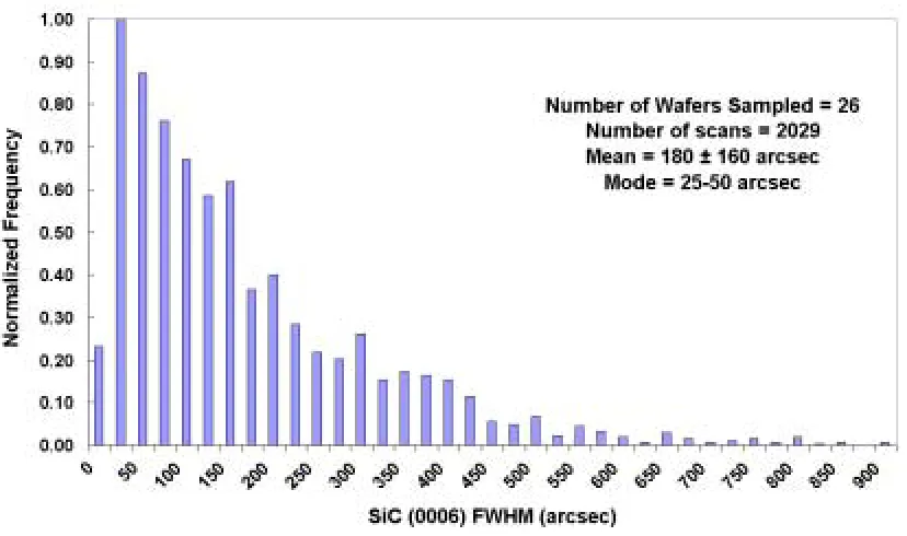
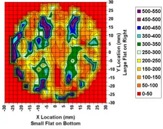
6H-SiC VariabilityFigure 3-1 shows a histogram of the range of FWHM values obtained in the maps of SiC(00.6) rocking curves of 26 randomly selected 50 mm diameter wafers. The values incorporate the entire spread of tilts in the crystal found in a given area. A large range of tilts can be present on a single wafer, as shown by the SiC(00.6) FWHM values in the scale of the rocking curves obtained from the contour map shown in Figure 3-2. Studies of numerous wafers do not show a pattern regarding the location of the regions, although it is common to observe symmetry in the patterns on a single wafer. Figure 3-3 shows that wafers taken from the same boule have similar map patterns, which indicates that the domain structures of the SiC propagate along the c-axis during growth. This similarity of wafers from the same boule also removes the possibility that the observed effects are due to surface polishing or other treatments prior to the x-ray measurements. It is postulated that because of this wafer-to-wafer similarity within a boule, treatment of the substrate surface via hydrogen etching or other methods will not change the domain structure present at the surface. Domain propagation through multiple wafers means that the domain structures are on the order of millimeters, or perhaps centimeters in size. Surface treatment does offer the benefits of polishing scratch removal and uniform step formation on the surface, but it will not change the overall structure of these large domains.
3.3.2
GaN Epitaxial Thin Films on 6H-SiCthe latter will incorporate the tilt characteristics of both the film and of the underlying wafer. As such, the use of FWHM values to compare two different experimental procedures for GaN growth must account for the variation in the SiC as well. This introduces an influential variable into all thin film rocking curve measurements on SiC wafers.
As shown in Figure 3-4, epitaxial GaN thin films do mimic the tilt of the underlying wafer. The GaN rocking curve is typically much smoother than that of the SiC, but never thinner. The distribution of tilts over the GaN film is similar to that of the SiC, but the former is much more regular and uniform. Distinctly separate GaN peaks typically only occurred in cases of extreme tilt between two or more regions in the SiC. The observed variability requires that the samples be scanned as broadly as possible. Typical triple axis x-ray measurements artificially lower the FWHM values for these samples by tightening the 2θ window below the actual range in the material. Rocking curves taken with optics that are more open are more useful to find poor areas of a film, but do not penalize good areas.
Changing the peak of interest to one that is off-axis reduces the limitations regarding the SiC correlation and measurement because the off-axis SiC values are typically much lower than the values for off-axis GaN, and they do not unduly influence the FWHM values of the GaN. This is illustrated in Figure 3-6 wherein the GaN (10.3) peak is contrasted with the SiC (10.9) peak. The SiC peak was chosen due to it’s proximity to the GaN peak in reciprocal space which allows the spot size and orientation to remain as constant as possible during the rocking curve measurement. The error in spot size differences is small for low order Bragg peaks; it increases with higher order off-axis peaks due to the increasing separation of the SiC and GaN peaks in reciprocal space. The uninfluenced (flat) portion of the data in Figure 3-6 is larger than in the analogous on-axis curves because the values of the off-on-axis FWHM are larger. Therefore, the GaN FWHM measurement is not influenced until the sample reaches approximately 400 arcsec in the SiC. The figure shows that the larger the divergence of the GaN FWHM from the SiC FWHM, the less measurement dependence there is on the SiC wafer variation. Since the off-axis scans are sensitive to edge dislocations, which are probably on the order of 1x10⁹ in these films, the influence of crystal tilt is less evident and the effect of dislocation broadening is more evident.
dislocation population in the film (edge, screw and mixed types), as determined by TEM for example. The absence of this latter information means that the population numbers one can predict are arbitrary, but still meaningful in a relative sense to samples grown under similar conditions.
3.3.3
Rocking Curve Improvement with Increased ThicknessIncreasing the thickness of GaN thin films is known to decrease the density of the threading dislocations through dislocation annihilation mechanisms.[6] Figure 3-7 shows the results of our analysis using the best-case FWHM values from numerous off-axis planes and subsequently plotting the data versus the inclination angle of the measured plane. Extrapolation of this data to an inclination angle of 90° yields an estimate for the pure edge dislocation content of the films. As mentioned previously, the character of the dislocation population must be known to make an accurate estimate of the true dislocation content in the films. If one assumes that the character of the dislocation population does not change significantly as the film grows thicker, it can be stated that our films have a decreasing dislocation density, as shown by the decreasing function value at an inclination of 90°.
in dislocation density, as measured in this study, is likely to be more significant than is shown.
Another point of note with regard to the sampling volume is that each Bragg peak used will have a different spot size due to the projection of the beam cross-section onto the tilted sample. Peaks with larger spot sizes will naturally have a larger number of substrate domains being sampled and thus appear to have more scatter and higher values if a poor area of the film is being interrogated. This effect is particularly noticeable in some higher order planes, such as the (10.1) or (20.1) planes, which have spot sizes that are roughly double that of the (00.2) peak. Alternatively, the (00.4) and (00.6) peaks have spot sizes that are 50% and 33% of the size of the (00.2) peak ,respectively.
3.3.4
Buffer Layer Effects on GaN Dislocation Populations3.3.4.1
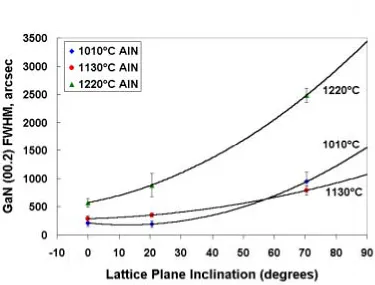
AlN Buffer LayersAlN grown at typical GaN growth temperatures (~1010 °C) is extremely pitted, however AlN grown at 1220°C is very smooth. SEM micrographs of the AlN surface prior to GaN overgrowth are shown in Figure 3-8. Using the techniques described above to graph the FWHM of GaN vs. the FWHM of the underlying SiC, extrapolating the data to a best-case value, and then graphing versus the inclination angle we obtain the results shown in Figure 3-9. It is interesting to note the large increase in predicted edge dislocation density in the high-temperature buffer layer sample. Prior to the experiment, we had hoped that a flatter, smoother surface would provide a better template for the subsequent growth of the GaN film, as was the case when going from a 1010°C buffer to the 1130°C buffer. In fact, the smooth surface is a detriment to the film with regard to edge type dislocation density. In order to reduce the density of threading dislocations created by the mechanism of island coalescence described above, it is necessary to reduce the number of nucleation locations on the buffer layer.
3.3.4.2
AlGaN Buffer LayersAs described above, the authors feel that any mechanism that reduces the density of islands in the initial growth stages of a GaN film will help to reduce the quantity of edge dislocations formed in the films by the subsequent reduction in twist boundaries. Growth of GaN on an AlGaN buffer layer reduces the GaN/Buffer mismatch between the layers by approximately 80% when using an Al0.2Ga0.8N buffer.[10] In addition, GaN
the ability to dope the layer, resulting in a conductive buffer layer for use in vertical device structures. As shown in Figure 3-10, the AlGaN buffer layer reduces the edge dislocation density of the GaN when compared with the best AlN buffer layer above.
3.4 Conclusions
6H-SiC wafers have a varied domain structure that strongly influences the measurement of GaN rocking curve values. The size of this influence makes it necessary to account for this variation when investigating GaN films via x-ray methods. The acquisition of numerous GaN FWHM data points with respect to the underlying SiC FWHM allows the investigator to obtain a “best-case” estimate of the GaN rocking curve values. This best-case value can be correlated with the values from other Bragg peaks to obtain dislocation population information as well as useful comparisons of the variables under study. This method has been used to show that GaN edge dislocation population decreases as a function of thickness when grown on 6H-SiC wafers.
through the reduce misfit between the GaN and AlGaN layer, or by reduction in the number of re-nucleation points of the GaN on the AlGaN.
3.5 References
1. B. Heying, X.H. Wu, S. Keller, Y. Li, D. Kapolnek, B.P. Keller, S.P. DenBaars, and J.S. Speck, Appl. Phys. Lett. 68, 5 (1996).
2. T. Metzger, R. Höpler, E. Born, O. Ambacher, M. Stutzmann, R. Stömmer, M.
Schuster, H. Göbel, S. Christiansen, M. Albrecht, and H.P. Strunk, Phil. Mag. A 77, 1013 (1998).
3. V. Srikant, J.S. Speck, and D.R. Clarke, J. Appl. Phys, 82 (1997) 4286-4295. 4. R.C. Glass, L.O.Kjellberg, V.F. Tsvetkov, J.E. Sundgren, and E. Janzen, Journal of Crystal Growth 132 (1993) 504-512.
5. H. Heinke, V. Kirchner, S. Einfeldt, and D. Hommel, Phys. Stat. Sol. (a) 176, 391 (1999).
6. S.K. Mathis, A.E. Romanov, L.F.Chen, G.E. Beltz, W. Pompe, and J.S. Speck, Phys. Stat. Sol. (a) 179, 125 (2000).
7. W.Qian, M. Skowronski, M. De Graef, K. Doverspike, L.B. Rowland, and D.K Gaskill, Appl. Phys. Lett, 66 (10) 1995.
8. X.J. Ning, F.R. Chien, P. Pirouz, J.W. Yang, M. Asif, Khan, J. Mater. Res. V11, (1996) p580.
9. X. H. Wu, L. M. Brown, D. Kapolnek, S. Keller, B. Keller, S. P. DenBaars, and J. S. Speck, J. Appl. Phys, 80 (1996) p. 3228.
BJ0363-02 BJ0363-04
BJ0363-05 BJ0363-07
Figure 3-6 – Off-axis GaN (10.3) FWHM vs SiC (10.9) FWHM. The higher FWHM of the off-axis GaN peak does not reach the SiC threshold until ~350”. The higher
Figure 3-7 – GaN edge dislocation estimation via inclination angle plot as a function of thickness of the GaN film.
Figure 3-10 – GaN edge dislocation estimation via inclination angle plot as a function of the buffer layer. The graded AlGaN buffer began at 1090°C and 20% Al
4.
Application of Nomarski interference contrast microscopy as a
thickness monitor in the preparation of transparent, SiC-based,
cross-sectional TEM samples
by
E.A. Preble, H.A. McLean, S.M. Kiesel, P. Miraglia, and R.F. Davis
Department of Materials Science and Engineering, North Carolina State University.
M. Albrecht
Institut für Werkstoffwissenschaften, Lerhstuhl VII, Universität Erlangen-Nürnberg.
D.J. Smith
Center for High Resolution Electron Microscopy, Arizona State University.
Abstract
4.1 Introduction
Techniques for the preparation of cross-sectional TEM samples of thin films are well documented [1,2] and include electro-chemical jet polishing, micro-cleaving, focused ion beam, and the sandwich/dimple method. The final method involves the creation of a sandwich of material that is thinned, dimpled, and finally ion milled to obtain an electron transparent region. The research reported herein has focused principally on enhanced control of sample preparation by this method via the development of an optical microscopy-based thickness measurement technique applicable to selected materials that are transparent to visible light. The specific materials and TEM samples of concern have been cross-sectional III-Nitride thin film/SiC substrate heterostructures with and without metal capping layers.
The high bond strength of SiC results in ion milling times longer than for most other materials of similar thickness. As such, excessive damage may accumulate in any softer films deposited on the SiC substrates. This can occur if the area of interest is not shielded from the milling beam or if the area of interest is too thick when milling is initiated.
same order as the thickness of the sample itself. To avoid over-dimpling, samples are often left too thick and require long ion milling times that may result in significant damage to both the SiC and any softer deposited films.
We have identified and improved several aspects of sample sandwiching and dimpling as well as utilized a Nomarski-enhanced, interference contrast-based, optical microscopy technique specifically for the measurement of thickness in dimpled and ion milled cross-sectional TEM samples of thin film/SiC substrate assemblies, but which should be generally applicable to other transparent materials. It is important to note that the initial observation of the interference fringes in a transparent material will be dependent on the light source, the lenses and the filters used in a given microscope. Moreover the appearance of the interference rings will occur in thickness ranges that depend on the transparent material under consideration. Additionally, the sample must be rotated in the microscope (see below) to determine the optimum position to observe the fringes. The following sections discuss the applicable interference contrast theory, detail the sample preparation procedure and describe the application of these techniques to specific SiC-based samples.
4.2 Interference Contrast Theory
needed to enhance the interference of the light so that the patterns are visible in thicker parts of the sample. Inserting a Nomarski prism into the light path splits the beam and significantly enhances both the interference effect on the light wave and the path difference of the light that reaches the sample. The two beams now strike the sample in areas that have a greater difference in thickness. When the light reflects from the sample, it again passes through the Nomarski prism and recombines. The phase difference is enhanced, and the interference fringes are visible at a larger sample thickness. Diagrams of the light path in a typical Nomarski-capable microscope and the schematics of a Nomarski modified Wollaston prism are published in references [3] and [4], respectively.
Light in the visible spectrum does not produce colors when transmitted through transparent materials; however, colors can be achieved that can be correlated with thickness by using Nomarski prisms in conjunction with a differential interference contrast (DIC) filter, reflected light and rotation of the sample. Interference contrast is a process by which refraction and reflection between two media in certain geometries can produce contrast effects visible to the observer.
Newton reported [5] and discussed interference fringes caused by two pieces of glass separated by air pockets. Newton created the diagram shown in Figure 1(a) after refining the experiment to be a lens on top of a glass sheet. While this diagram does not illustrate refraction effects inside a wedge-shaped material, it does capture the essence of interference contrast. Figure 1(b) shows a modern day photo of “Newton’s rings”, in a configuration similar to those observed by Newton.[6]
any transparent material. The schematic diagram shown in Figure 2 illustrates the mechanism of interference from a thin transparent wedge. The path length difference of the light that reflects from the top surface of the sample (beam 1) causes it to interfere with the light that refracts into the material (beam 2), reflects off of the bottom of the sample, and emerges from the sample in the same location. The interference, whether constructive or destructive, produces lines (or lack of lines for destructive interference) on the observation plane that corresponds to the thickness of the wedge. If the wedge is uniform and the thickness change constant, very regular lines are produced. Such lines are called fringes of equal thickness. In the case of a dimpled TEM sample, the fringes of equal thickness are actually rings of equal thickness due to the circular geometry of the dimple.
4.3 Experimental Details
4.3.1
Materials and Equipment4.3.2
Cross-Sectional TEM Specimen Preparation and ObservationThe sandwich method was employed in this research. Two 1mm wide slices were initially cut from the aforementioned samples; as were two 1mm wide pieces of sapphire for structural support. A small amount of Gatan G1, or similar, epoxy was applied to the contacting surfaces and each piece was then assembled into a sandwich with the thin film surfaces facing each other, and the sapphire pieces positioned on the outside.
In order to obtain a very thin gap between the two facing film surfaces the sandwich and was cured at 120ºC for 30 minutes compressed in a small vise made of Teflon®. The small gap will protect this thinnest region from ion damage by reducing the line-of-sight access of the ion mill beam in this part of the sample. Teflon® worked well as a vise material as it did not bond strongly to the epoxy. Care was taken to not over tighten the vise, as Teflon® creeps at relatively low temperatures, and vise damage can result on the sample faces on which the pressure is applied.
Each sandwich was subsequently diced into 2mm pieces for mounting to a TEM sample ring. The surface of each piece was flattened by grinding with a 30µm grit diamond embedded film and then polished using progressively higher grit diamond until a 0.1µm polish was obtained. The polished face was then mounted to a standard TEM sample ring, e.g. a 1GC12H Pelco slotted copper ring. A uniform, exceptionally flat surface with a high polish was necessary, as the desired final sample thickness ~1-2µm.
dimpler, the glass peg was then marked with respect to the orientation on the dimpler stage so that the sample could be removed and replaced without re-alignment.
The samples were dimpled with a copper wheel using 3µm diamond paste and were periodically removed to look for interference fringes in the optical microscope. Interference patterns (rings) comprised of a repeating sequence of red and green bands followed by a rainbow sequence initially appeared in the SiC substrates (the nitride and Au films were much too thin in cross section to allow observation of interference patterns in the optical microscope) when the thickness of the thinned region was >10-15µm. It is important to note that the dimpled samples must be rotated on the microscope table until the interference colors appear. It was also possible to observe rings in the sapphire support posts at a greater thickness than in the SiC; this provided an alert that the samples were close to the desired thickness.
Once the rings appeared in the samples, the grinding weight was halved. Once the yellow ring appeared, the weight was reduced to a very low setting (5 on the Gatan dimpler). With the appearance of the second yellow ring, the copper dimpling wheel was replaced by a felt polishing wheel, with the continued use of the 3µm diamond paste. The polishing was deemed complete when scratches were no longer visible in the region of interest. Thinning was not usually continued beyond the second yellow ring, as sample breakage became likely.
frequently interrupted and the samples examined in the optical microscope to prevent over-milling. A large area of very thin material in the pre-milled sample can cause large holes to open quickly during ion milling. A second set of fringes having thinner rings than the previous fringes appeared prior to and on the edges of any perforation that occurred.
4.4 Application of Interference Contrast for Thickness Determination
4.4.1
GaN/AlN/ 6H-SiC(0001) StructuresNomarski images of a SiC sample with AlN/GaN layers (not visible at this magnification) grown on it, after being thinned to <1µm, are shown in Figure 3. The sequence of repeating red and green bands followed by a rainbow sequence is shown in Figure 3(a). Also shown in this figure is the importance of the previously noted sample rotation on the microscope table in terms of the intensity of the interference fringes. The observed intensity of the fringes is seen to change when turned from an orientation where the epoxy line was oriented at 45º from vertical to where it was oriented vertically in the field of view. It is not clear whether the intensity change is due to a polarization effect in the sample, or due to the directional nature of the Nomarski prism and the differential interference contrast (DIC) filter.
Figure 6 shows the secondary set of interference fringes (see enhanced rectangle) in a sample that has been milled to perforation. These small order fringes are indicative of material that is typically thin enough to be electron transparent. It is also possible to observe the AlN/GaN film on the surface of the SiC, running left-to-right in the center of the photo. The small pits visible in this figure are indicative of ion milling damage. Samples that were milled for long periods of time (>4) hours had extensive pitting that degraded the quality of the TEM images.
4.4.2
Metal/thin film heterostructure/substrate assemblyThe thickness of transparent, SiC-based, cross-sectional, TEM samples has been correlated to the color of the interference patterns (rings) observed via Nomarski differential interference contrast optical microscopy under reflected light conditions. The Nomarski prism allowed observation of contrast rings when the thickness of these samples was within the 1-20 µm range. This significantly improved the accuracy of dimpling, reduced sample breakage due to over-dimpling, and also reduced sample damage due to over ion milling of under-dimpled samples. The use of a Teflon® vise to apply pressure to the samples during curing of the epoxy reduced the width of the resulting epoxy line that shielded the film surface more effectively from ion milling damage. The technique is also applicable for the analogous preparation of other transparent materials where fringes have been observed, such as zinc oxide and sapphire.
4.5 Acknowledgements
4.6 References
1. J. Elect. Micrs. Tech. 1, 53-61, 1984.
2. Specimen preparation for transmission electron microscopy of materials. Bravman, Anderson, McDonald, MRS symposium proceedings, v115, Pittsburgh PA, 1988. 3. P.C. Robinson and S. Bradbury, Qualitative Polarized-Light Microscopy, Oxford University Press, Royal Microscopy Society, 1992. (see Fig 7.3)
4. S. Bradbury and P.J. Evennett, Contrast Techniques in Light Microscopy, BIOS Scientific Publishers and the Royal Microscopy Society, 1996. (see Fig 7.6)
(a) (b)
Figure 4-1 – (a) Newton's Fringes, as theorized by Newton[5] and (b) a modern day photo of Newton’s fringes created by a curved lens on top of a glass sheet.[6]
Figure 4-3 - Effect of sample rotation on the intensity of the interference fringes. The exposure of photo (a) was 0.002 seconds, while the exposure of photo (b) was 0.25 seconds (125 times longer). Note the repeating red/green pattern of the larger (thicker material) rings in photo (a), which progress to a rainbow pattern as the sample thins. The white material is <1µm thick.
Figure 4-5 - Thickness measurements of SiC correlated to Nomarski fringes
5.
Correlation of the Electrical Properties and the Structural and
Microstructural Characteristics of Deposited and Annealed Pt and
Au Contacts on Chemical-vapor-cleaned GaN Thin Films
by
E.A. Preble, K.M. Tracy, S. Kiesel, H. McLean, P.Q. Miraglia, R.J.
Nemanich, and
R.F. Davis
Materials Science and Engineering, North Carolina State University, Raleigh, NC 27695.
M. Albrecht
Institut für Werkstoffwissenschaften, Lerhstuhl VII, Universität Erlangen-Nürnberg.
D.J. Smith
Center for High Resolution Electron Microscopy, Arizona State University.
Abstract
5.1 Introduction
Physical and chemical degradation of the metal contacts employed in devices based on the (Al, Ga, In)N system are likely to occur under their anticipated operating conditions.[1] Pt and Au are promising candidates for Schottky contacts on n-type GaN because of their high work functions and chemically inert nature. Variability in the electrical results of metal contacts can be attributed to differences in surface preparation which will leave varying levels of contamination or insulating material on the surface of the GaN prior to contact deposition.[2]. A primary goal of these studies was a significant reduction in the variability in the surface preparation by using in situ cleaning and contact deposition. A chemical-vapor-cleaning (CVC) procedure was developed that removed all detectable hydrocarbon and oxygen contamination from the GaN surface. Subsequent deposition of either the Pt or the Au was conducted prior to removal from the ultra-high-vacuum system.
This study focuses on the structural and microstructural characteristics of thin Pt and Au films deposited on Si-doped, n-type, monocrystalline GaN(0001). Particular attention is paid to the metal/GaN interface in the as-deposited state and after annealing under ultra-high vacuum. Experimental approaches used in this research are discussed and correlated the electrical results and the physical and chemical changes observed within the contacts and the metal/GaN interfaces as a function of heat treatment.
5.2 Experimental Details
6H-SiC(0001) wafers on which had been previously deposited a ~0.1µm thick buffer layer of AlN or Al0.2Ga0.8N. The films were doped with Si to an ionized donor concentration (ND
-NA) of 1·1017 cm-3. They were subsequently diced into 15mm square samples. Surface
cleaning prior to vacuum insertion consisted of sequential immersion in trichloroethylene, acetone, and methanol, followed by a 10-minute dip in 49% hydrochloric acid. A chemical vapor cleaning (CVC) process was developed for in situ surface preparation and involved annealing the GaN samples in an ammonia atmosphere at a surface temperature of 860°C for 15 minutes.Atomic force microscopy revealed the RMS surface roughness before and after the CVC processing to be 5-10Å. Auger results showed the stoichiometry of the Ga-terminated (0001) surface to be the same before and after the cleaning procedures. Thus, the CVC cleaning process neither roughened the surface nor changed its chemistry. Details of this process have been published separately.[3,4] The samples were subsequently transferred under ultra-high vacuum to the metal deposition chamber and coated with either 1200Å of Au or 600Å of Pt.
The growth mode of the Pt and Au films was determined using the method of Sitar et al.[5] and King et al.[6] for growth of AlN and GaN films. A special set of Pt and Au films was initially and individually deposited in a step-wise manner of increasing thickness over two entire GaN surfaces. The accumulated thickness values for the Pt were 2, 3, 5, 10, 15, 20, and 700 Å; the analogous values for the Au were 2, 3, 5, 10, 12, 17, 20, 25 and 770 Å. X-ray photoelectron spectroscopy (XPS) data was collected using a Fisons-VG Scientific system after each deposition. Specifically, the intensities (area) of the XPS core levels of the uncoated GaN sample (Io) were compared with the intensities
obtained by plotting the Is/Io ratios as a function of thickness. The mode of growth of then determined by comparing these plots with theoretical plots of the thermodynamically controlled modes of growth.
The 700 Å thick Pt samples and the 770 Å thick Au samples from the aforementioned studies were removed from vacuum, diced to produce 7.5mm square samples that were patterned using a two-step photolithography process. The first step involved formation of the Schottky contact pads; the second step involved formation of the ohmic contact rings of either Al or Ti(700Å)/Au(300Å) deposited via thermal and electron beam evaporation, respectively, and surrounding the Schottky pads. The respective ohmic contacts were used for the as-deposited and annealed samples. The photoresist was subsequently removed. The resulting pattern was a series of exposed ring-shaped regions. The contacts were then rapidly thermally annealed in a N2 ambient
for 3 minutes at the individual temperatures of 400°C, 600°C, or 800°C.
5.3 Results
5.3.1 As-Deposited Contacts
The plot of the Is/Io ratios as a function of thickness is shown in Fig. 1. This figure also shows theoretical curves for the thermodynamically-controlled two-dimensional (Frank-van der Merwe), three-two-dimensional (Volmer-Weber ) and mixed two- and three-dimensional (Stranski-Krastanov) modes of film growth. The data for both Pt and Au agree well with the two-dimensional model.
Scanning electron microscopy images revealed a smooth, featureless surface for both metals, as shown in Fig. 2. Cross-sectional high-resolution (HR) TEM micrographs taken from the metal/GaN interfaces are shown in Fig. 3. These micrographs and the analyses of associated diffraction patterns showed that both metals were single crystal and epitaxial, with a (111)metal//(0002)GaN orientation relationship with the GaN. The
interfaces were abrupt and smooth, with no visible reactions or mixing in either the Pt or the Au contacts. Numerous twinning defects were observed in both materials, but no other significant structural defects were observed that would alleviate the mismatch strain between the metal layers and the GaN film. X-ray diffraction analysis shown later also corroborated the single crystal nature of the films, as well as the (111) growth orientation.
5.3.2 Annealed Contacts
the Pt and the Au contacts, respectively. Annealing of the contacts gave the principal result that the rectifying behavior of the contacts was degraded, eventually becoming ohmic after annealing at 600 or 800°C, as shown in Fig.4.
The scanning electron micrographs shown in Fig. 5 of the metal surfaces after annealing at 800°C reveal a loss of structural integrity in the surface of the Pt contacts; whereas, the Au contacts remained intact and smooth. Liu et al.[7] and Gasser et al.[8] observed that holes formed in their Pt films on GaN due to the formation of nitrogen gas which accumulated under the Pt surface and eventually escaped through perforations of the platinum layer. Although GaN does not dissociate in vacuum until above 800°C, formation of nitrogen is accelerated by the reaction of Pt and GaN to form Ga2Pt and
N2.[9] Our data agrees with that reported in the literature, however, the reactions visible in our samples were less severe due to the shorter annealing times of 3 minutes, rather than 30-120 minutes, as reported by other investigators. For example, Liu et al.[7] reported complete degradation of the Pt contacts after annealing at 400°C for 120 minutes, in contrast to our 400°C sample which showed increased leakage currents, but was not yet ohmic after 3 minutes at 400°C.