Closed Loop Simulation of an Active
Buck-Boost Inverter
Sreeja Sreeram1, Susmi.K.M2, Sreelakshmi Suresh 3
PG Student [Power Electronics], Dept. of EEE, Vidya Academy of Science & Technology, Thrissur, Kerala, India 1
PG Student [Power Electronics], Dept. of EEE, Vidya Academy of Science & Technology, Thrissur, Kerala, India2
PG Student [Power Electronics], Dept. of EEE, Vidya Academy of Science & Technology, Thrissur, Kerala, India3
ABSTRACT: Renewable energy resources are gaining popularity now a days. Their input varies with changes in climatic conditions. So the output from them is not a constant value. The output of the energy sources have to be connected to grid. But the grid voltage is always constant. So the output from the renewable energy converters have to be constant. But the input of the renewable energy converters always varies with climatic and weather conditions. So the output of the converters also changes. To get a constant output voltage at the grid some power converters have to be connected in between the renewable energy converters and the grid. These converters maintain constant output voltage at constant frequency irrespective of changes in input voltage. This paper introduces the concept of an Active Buck-Boost Inverter (ABI). In this converter the passive elements from the conventional buck-boost converter is eliminated. Closed loop simulation of the proposed converter is done to show that the output voltage of the converter remains the same even if the input voltage changes.
KEYWORDS: Active Buck-boost Inverter (ABI), DC/AC unit, AC/AC unit
I.INTRODUCTION
The world is facing energy crisis now a days. Non-renewable energy resources are getting used up very fast. So renewable energy resources are gaining popularity now. The most popular renewable energy resource is solar energy. Photovoltaic cells (PV) are used to harvest solar energy. PV cells convert the solar radiation to DC form of electrical energy. Their output have to be given to the grid. The grid provides a fixed voltage fixed frequency AC power all the time. So the output from the PV cells have to be converted suitably to connect it with the grid. The output from the PV cells varies with climatic and weather conditions. In morning and evening time the solar radiations are very feeble. In night it is almost zero. In noon time the solar radiation is maximum. So we can see that the input to the PV cell is not a constant. So the output also varies. The output voltage from the PV cells will be maximum when the solar radiation is higher and the output will be minimum when the radiation is lower. So the output from the PV cell array have to be made constant so that they can be connected to the grid. Also the output from the PV cell array is a DC value. So the DC voltage have to be converted to AC voltage for connecting it to the grid. So we require a power converter i.e. a DC/AC converter. Also the power have to be modulated. If the output voltage from the converter is less than the grid voltage then it have to be stepped up (boost). If the output voltage from the converter is higher than the grid voltage then it have to be stepped down (buck). So there have to be a power modulator. Conventional power converters have one DC/AC inverter and the AC/AC power modulator. So they require two stage operation.
II.CIRCUIT DIAGRAM
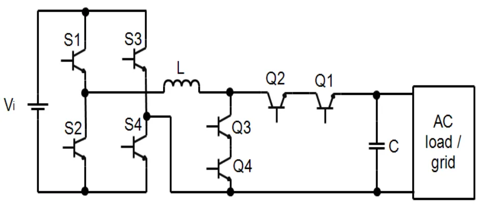
Fig.1 shows the circuit diagram of the Active Buck-Boost Inverter. It have two sections for bucking and boosting the voltage. It have the conventional H-bridge inverter section with four switches. This section of the inverter is connected to the input. The input is variable DC voltage. The output of the H-bridge is a reduced AC voltage. The output of this H-bridge is connected to the Active part of the inverter. The active part does the boosting of the voltage. The switches in the H-bridge is controlled by using SPWM technique. The switches in the active part is controlled by duty ratio control.
Fig 1: Circuit Diagram of Active Buck-Boost Inverter
The output of the Active Buck-Boost inverter is connected to the grid. So the output of the inverter is controlled according to the grid requirement.
III.MODES OF OPERATION
There are two modes of operation-buck and boost mode. SPWM control strategy is applied on the H-bridge side. Output voltage of the H-bridge side can be expressed as
V= MVi sinωt
Where M is the modulation ratio and Vi is the input DC voltage.
The H-bridge part and the active part share the same inductor and capacitor. In the active part the switches are controlled by duty ratio control. Referring to Fig.1 in the active part switches Q2 and Q4 are always on and Q1 and Q3
are modulated in complementary in the output positive half cycle. In the output negative half cycle Q1 and Q3 are
always on while Q2 and Q4 are modulated in complementary. The output voltage is given by:
vo=V/(1-d)= MVi sinωt/(1-d)
,where d is the duty ratio of Q3 in output positive half cycle or duty cycle of Q4 in output negative half cycle.(1-d) is
equated as d’ where d’ is the duty ratio of Q1 in output positive half cycle or duty cycle of Q2 in output negative half
I. Buck Mode: When the input voltage is higher than the required DC voltage needed to obtain the grid voltage the inverter operates in the buck mode. Voltage is stepped down here. In this mode d’ is set to 1 or d is set to zero. So Q1
and Q2 are always in on condition and Q3 and Q4 are switching in grid frequency. The output voltage is given as:
vo= MVi sinωt
Thus in buck mode by varying modulation ratio “M” between 0 to 1 the output is controlled.
II.Boost Mode: When the input voltage is not enough to obtain the desired grid voltage then the inverter works in the boost mode. Here “M” is set to 1 and “d’”is adjusted to boost the voltage. The output is now given as:
vo= Vi sinωt/d’
IV.CLOSED LOOP SIMULATION AND RESULTS
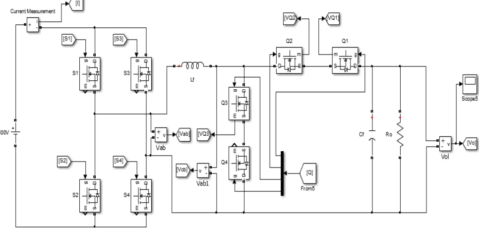
The closed loop circuit with feedback is implemented in MATLAB and is simulated to obtain the desired results.
Fig 2: Closed loop MATLAB circuit of Active Buck-Boost Inverter
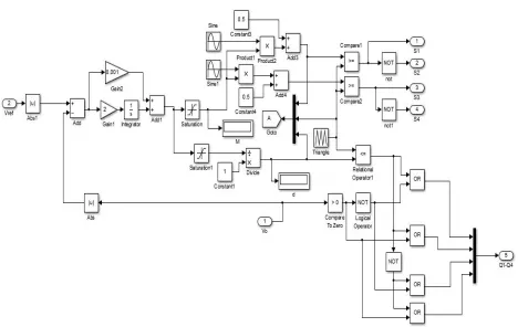
Fig 3: Simulation Diagram of Control Circuit
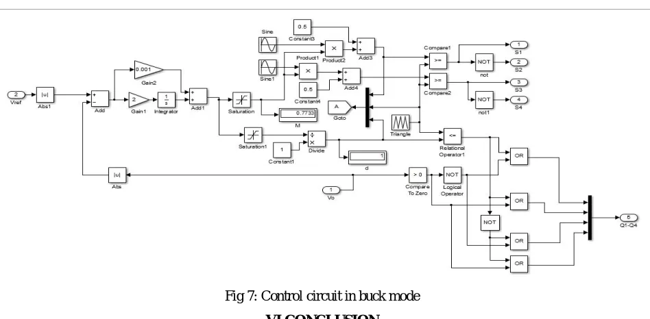
The backbone of the active buck-boost inverter is its control circuit. The control circuit simulated is a closed loop circuit in MATLAB. Control signal for each switch is generated from the control circuit. For simulating the closed loop circuit feedback is required. The output voltage is fed back. A reference voltage Vref is set. The voltage feedback is
compared with the reference voltage. If the output voltage is less than the reference voltage then boost command is generated. If the output voltage is above the reference voltage then buck command is generated. The gating signals to the switches are generated according to the mode of operation i.e. buck mode or boost mode. It is implemented by a combination of logic gates. Switches in the H-bridge section-S1,S2,S3 and S4 are controlled by SPWM technique. So
modulation ratio “M” is controlled for controlling gating signals to these switches. Duty ratio is controlled for switches Q1,Q2,Q3 and Q4. For implementing closed loop control a PI control is designed. The value for proportional gain is
0.001 and integrator gain is 2. The value is designed is through trial and error method. Two values of saturation levels have to be set because there is a lower voltage level for buck mode and there is an upper voltage level for boost mode. Sine wave and triangle wave is compared for generating SPWM control signals. By varying the amplitude of sine wave the modulation ratio “M” is controlled. A bias value of 0.5 is given for sine wave to make it stable. The values of “M” and “d” will be displayed during simulation.
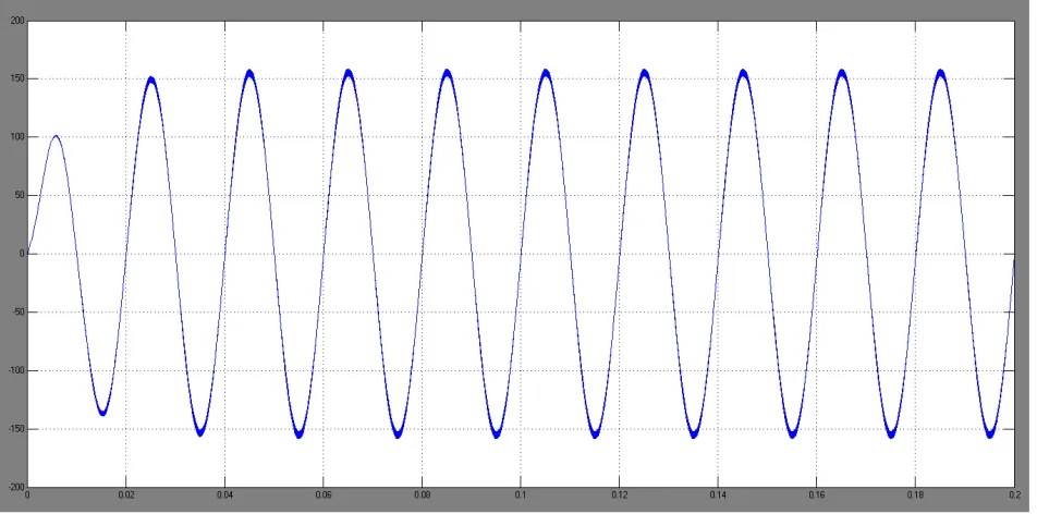
Fig 4: Output voltage in boost mode
Fig 5: Control circuit in boost mode
Fig 6: Output waveform in Buck mode
Fig 7: Control circuit in buck mode
VI.CONCLUSION
The closed loop circuit of Active Buck-Boost Inverter is implemented and simulated in MATLAB. The output is also verified. By properly designing the feedback circuit and the PI controller the closed loop control can be implemented. This closed loop circuit if implemented practically will be a true asset for the energy field. It will find a wide application in renewable energy source filed especially in solar energy harvesting.
REFERENCES