INEQUALITY CONDITION FOR GRATING LOBES OF PLANAR PHASED ARRAY
C.-H. Liang, L. Li, and X.-J. Dang
National Laboratory of Antennas and Microwave Technology Xidian University
Xi’an 710071, China
Abstract—This paper presents a general inequality for the grating lobes of the planar phased array, whether rectangular lattice or triangular lattice. And for the planar phased array with grating lobes, the maximum scanning angle is given.
1. INTRODUCTION
Phased array is an important kind of array for its flexibility, speed and multiple beams. In the theory, it is grating lobes and blindness that mainly restrict the performance of arrays, and blindness results from the coupling between array elements. Ref. [1] shows that the study of center elements active pattern can reveal the feature of blindness. The corresponding physical concept is the coupling between elements prevents the center elements radiating power at a certain angle. But a further research shows the conclusion only applies to infinite or large arrays. Otherwise the coupling difference between the center and edge elements makes the center elements uncommon and changes the feature of blindness. Ref. [2–4] clearly shows grating lobes are a consequence of the periodicity of the array pattern and depend on the arrangement of the elements.
This paper introduces the general normalized parameterAandB
2. INEQUALITY CONDITION FOR GRATING LOBES
In this paper, the planar array lies in XOY plane. And (θ, ϕ) shows the field or pattern at (θ, ϕ), (θ0, ϕ0) defines the angle to which main
beam is scanned. We defineϕ0= 90◦ asEplane andϕ0= 0◦H plane.
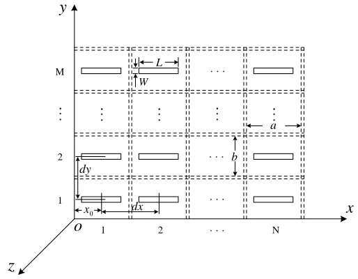
The discussion of the grating lobes are based on the rectangular lattice and the triangular lattice. The rectangular lattice is shown in Fig. 1, where the element distance is dxand dy.
x y
z
o
1 2 N1 2 M
.
dx dy
0
x
L
W
a
b
.. ... ... ... ...
. . .
. . .
. . .
. . .
Figure 1. Phased array of rectangular lattice.
The array pattern for the array of isotropic radiators excited with equal amplitude [1] is
S(θ, ϕ) =
m
ejmkdx(sinθcosϕ−sinθ0cosϕ0)·
n
ejnkdy(sinθsinϕ−sinθ0sinϕ0)
(1)
Obviously, the maximum condition [1] for Eq. (1) is
sinθcosϕ= sinθ0cosϕ0+ p
dx, (p= 0,±1,±2,· · ·)
sinθsinϕ= sinθ0sinϕ0+ q
dy, (q= 0,±1,±2,· · ·)
(2)
wheredx=dx/λ,dy=dy/λ, and when
θ = θ0, ϕ= ϕ0, which is the main beam angular position. So p and q can not simultaneously equal 0 under the condition of grating lobes’ existence.
Figure 2 shows the triangular lattice, where the element distance isdx anddy. The array pattern [2] is as follows.
x y
z
o dx
dy
Figure 2. Phased array of triangular lattice.
S(θ, ϕ)=
1 +ej12kdx(sinθcosϕ−sinθ0cosϕ0)ejkdy(sinθsinϕ−sinθ0sinϕ0)
·
m
ejmkdx(sinθcosϕ−sinθ0cosϕ0)·
n
ejnkdy(sinθsinϕ−sinθ0sinϕ0) (4)
The maximum condition [2] is
sinθcosϕ= sinθ0cosϕ0+ p
dx, (p= 0,±1,±2,· · ·)
sinθsinϕ= sinθ0sinϕ0+ q
2dy, (q = 0,±1,±2,· · ·) p+q= even
(5)
The last equation is the even restriction condition for triangular lattice. This paper introduces the normalized parameter Aand B.
A= p
B =
q
dy rectangular lattice q
2dy triangular lattice
(6)
Thus, Eq. (2) and Eq. (5) can be united as
sinθcosϕ= sinθ0cosϕ0+A
sinθsinϕ= sinθ0sinϕ0+B
(7)
Squaring Eq. (7) and considering that the grating lobes begin to form atθ= 90◦ and sinθ= 1 [2], we can obtain
sin2θ0+ 2 sinθ0(Acosϕ0+Bsinϕ0) + (A2+B2−1) = 0 (8)
Equation (8) shows the position of the main beam θ0, ϕ0 when the
grating lobes begin to form. We introduce
cosϕ1= A √
A2+B2
sinϕ1 = B √
A2+B2
(9)
Equation (8) can be simplified as
sin2θ0+ 2
A2+B2cos(ϕ
0−ϕ1) sinθ0+ (A2+B2−1) = 0 (10)
Let
ξ=A2+B2cos(ϕ
0−ϕ1) η=ξ+ sinθ0
(11)
The corresponding domain is
sinθ0∈[0,1]
ξ ∈
−A2+B2,A2+B2
η ∈
−A2+B2,1 +A2+B2
(12)
And Eq. (10) can be changed into two hyperbolic equations
ξ2−η2 =A2+B2−1, when A2+B2−1>0
or
0
1
1
-2 2
1+ A +B
2 2
B A +
2 2
B A +
2
2 B
A + 1
- ξ
η
η = ξ + 1
η = ξ
-Figure 3. Hyperbolic curves and domain of grating lobes.
The hyperbolic curves and domain of grating lobes are shown in Fig. 3.
Obviously, no crossing point between hyperbolic curves and domain is the condition for no grating lobes. Let
η=ξ+h
h >1 (14)
where h >1 assures no crossing point between hyperbolic curves and domain.
The research shows only considering the first equation of Eq. (13) is sufficient. Substituting Eq. (14) into Eq. (13), we can obtain
ξ2−(ξ+h)2=k
k=A2+B2−1>0 (15)
Only whenξ <0, Eq. (15) can hold. And when Eq. (15) can not hold, the grating lobes can also not exist. So we obtain
Its solution is
h=|ξ| ±|ξ|2−k >1 (17)
When the negative root meets the inequality, the positive one automatically meets the inequality. That is|ξ| −|ξ|2−k >1 or
|ξ|2−k <|ξ| −1 (18)
Squaring Eq. (18), we obtain
A2+B2 >2|ξ| (19)
Considering|ξ|=√A2+B2|cos(ϕ
0−ϕ1)|and the modulus of circular
function less than 1, we can obtain the condition for no grating lobes of planar phased array
A2+B2 >4 (20)
where A and B must be out of the circle with radius 2, as shown in Fig. 4.
B
A
0
z
Figure 4. Circular domain inequality forAandBunder the condition without grating lobes.
The distance condition for elements under different lattice will be given.
Inequality condition for no grating lobes is p dx 2 + q dy 2
>4 (21)
We must consider all the possibility of p = 0,±1,±2,· · · and q = 0,±1,±2,· · ·. In fact, we only need consider two worst cases:
when (p, q) = (1,0),
1
dx
>2,dy unconfined
and
when (p, q) = (0,1),
1
dy
>2,dx unconfined
So, the distance condition for no grating lobes of rectangular lattice is
dx <0.5, dy <0.5 (22)
Case 2 Triangular lattice
Inequality condition for no grating lobes is
p dx 2 + q 2dy 2
>4 (23)
We must consider all the possibility of p = 0,±1,±2,· · · and q = 0,±1,±2,· · ·. In fact, we only need consider three worst cases:
when (p, q) = (2,0),
2
dx
>2,dy unconfined
and
when (p, q) = (0,2),
1
dy
>2,dx unconfined
When (p, q) = (1,1), we notice that inequality condition for no grating lobes have many distribution. The physical concept shows the distance
dxand dy is contradictory.
1 dx 2 + 1 2dy 2
>4 (24)
Considering the restriction (2, 0) and (0, 2), we obtain the optimum restriction 1 dx 2 >3 1 2dy 2
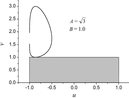
So A = √3, B = 1. Thus the optimum distance inequality for the triangular lattice is
dx <√3/3 = 0.57735, dy <0.5 (26)
Obviously, the element distance for no grating lobes of triangular lattice is larger than the rectangular lattice, which mainly lies in dx. Letu= cosϕ0andv= sinθ0, we obtain the optimum element distance
lies out of grating lobes, as shown in Fig. 5.
-1.0 -0.5 0.0 0.5 1.0
0.0 0.5 1.0 1.5 2.0 2.5 3.0
3 =
A
v
u
B = 1.0
Figure 5. Optimum element distance lies out of grating lobes.
3. MAXIMUM SCANNING ANGLE maxθ0
In many practical engineering, many restriction makes Eq. (2) unhold. Then grating lobes are unavoidable. We defines scanning angle ϕ0 ∈
[0,2π] andθ0∈[0,maxθ0] for planar phased array in which the domain
without grating lobes are called maximum scanning domain and maxθ0
is maximum scanning angle, as shown in Fig. 6.
We define u = cosϕ0 and v = sinθ0. Fig. 7 shows the classical
case with grating lobes, where u∈[−1,1],v∈[0,1]. Eq. (8) can be written as
v2+ 2v
Au±B1−u2+ (A2+B2−1) = 0 (27)
x
y
z
0
max
0
θ
Figure 6. Maximum scanning domain and maximum scanning angle.
u
v
1 1
1
- 0
0 =
du dv
v
max
Figure 7. Maximum scanning domain with grating lobes maxv
corresponding to dvdu = 0.
Differentiating Eq. (27)
2vdv du+ 2
dv du
Au±B1−u2+ 2v
A∓B√ u
1−u2
= 0 (28)
extreme is
A=±B√ u
1−u2 (29)
Squaring Eq. (29), we can obtain
u=±√ A
A2+B2 (30)
Select the negative root, then
u=−cosϕ1 (31)
The equation for extreme is
v2−2A2+B2v+ (A2+B2−1) = 0 (32)
Finally, we can obtain
maxv=A2+B2−1 (33)
that is
maxθ0 = sin−1
A2+B2−1 (34)
No crossing points exist between another root of Eq. (32) and grating lobes, so we ignore it. Eq. (14) shows the maximum scanning angle maxθ0. From Eq. (33), we can obtain when
A2+B2−1>1 (35)
the grating lobes do not exist. We find Eq. (3) equal to Eq. (20). When √A2+B2 − 1 < 0, no scanning domain exists, which
accounts for the ignorance of the second hyperbolic curve of Eq. (13). Fig. 8 shows whenA= 1.16686, the variation of the maximum scanning angle withB.
Figure 9 shows the pattern of 20× 20 triangular lattice with
dx= 1.008λ,dy= 0.504λ. Fig. 9(a) shows the pattern without phase shift. Fig. 9(b) shows the pattern of ϕ = 0◦ when the main beam is
θ0= 60◦,ϕ0= 0◦. According to Eq. (23), there is grating lobes under
this condition. But it is evidence that no grating lobe exists on this plane. From Fig. 9(c) (ϕ = 82.7◦), one can see the grating lobe. It is concluded that the main beam and the grating lobe can lie on two different planes. The maximum scanning angle θ0 = 23.765◦ can be
-1.0 -0.5 0.0 0.5 1.0 0.00 0.25 0.50 0.75 1.00 =64.21 0 =40.55 0 =32.82 0 =24.50 0 A=1.16686 B=0.5 B=0.8 B=1.008 B=1.16686 B=1.5 u v =15.63 0 θ θ θ θ θ O O O O O
Figure 8. Variation of the maximum scanning angle with B, A = 1.16686.
-100 -80 -60 -40 -20 0 20 40 60 80 100 0.0 0.2 0.4 0.6 0.8 1.0 S θ λ 008 . 1 = dx 504 . 0 = dy
-100 -80 -60 -40 -20 0 20 40 60 80 100 0.0 0.2 0.4 0.6 0.8 1.0 S o o o 0 0 60 0 0 = = = ϕ θ
-100 -80 -60 -40 -20 0 20 40 60 80 100 0.0 0.2 0.4 0.6 0.8 1.0 S o o o 45 225 765 . 23 0 0 = = =
-100 -80 -60 -40 -20 0 20 40 60 80 100 0.0 0.2 0.4 0.6 0.8 1.0 S o o o 7 . 82 0 60 0 0 = = = θ θ θ ϕ ϕ θ ϕ ϕ θ ϕ λ (a) (b) (c) (d)
Figure 9. Pattern of phased array of triangular lattice. (a) θ0 =
4. CONCLUSION
On the basis of study on all kinds of arrangement of planar phased array, this paper presents general normalized parameterAandB, and proves under the condition for no grating lobes A and B meet circle domain inequality
A2+B2 >4
Distance condition for rectangular lattice is dx < 0.5 and dy < 0.5, and the optimum distance condition for triangular lattice is dx < √
3/3 = 0.57735 and dy < 0.5. On the other hand, when domain inequality does not hold, the maximum scanning angle is maxθ0 =
sin−1
√
A2+B2−1. The numerical computations show that the
conclusions can also applied to the arrays with unequal amplitude. The research on blindness of phased array will be reported later.
REFERENCES
1. Amitay, N., V. Galindo, and C. P. Wu, Theory and Analysis of Phased Array Antennas, Wiley-Interscience, 1972.
2. Sharp, E. D., “A triangular arrangement of planar-array elements that reduces the number needed,” IRE Trans. Antennas and Propagation, 126–129, March 1961.
3. Stark, L., “Microwave theory of phased-array antennas — A review,” Proceedings of IEEE, Vol. 62, No. 12, 1661–1701, Dec. 1974.
4. Pozar, D. M. and D. H. Schaubert, “Scan blindness in infinite phased arrays of printed dipoles,” IEEE Trans. Antennas and Propagation, Vol. 32, No. 6, 602–610, June 1984.
5. Wheeler, H. A., “The grating-lobe series for the impedance variation in a planar phased-array antenna,” IEEE Trans. Antennas and Propagation, 825–827, Sep. 1965.
6. Wheeler, H. A., “The grating-lobe series for the impedance variation in a planar phased-array antenna,” IEEE Trans. Antennas and Propagation, Vol. 14, No. 6, 707–714, Nov. 1966. 7. Diamond, B. L., “A generalized approach to the analysis of infinite
planar array antennas,” Proceedings of IEEE, Vol. 56, No. 11, 1837–1851, Nov. 1968.
9. Vescovo, R., “Beam scanning with null and excitation constraints for linear arrays of antennas,” Journal of Electromagnetic Waves and Applications, Vol. 21, No. 2, 267–277, 2007.
10. Vallecchi, A. and G. B. Gentili, “Broad band full scan coverage dual polarised spherical conformal phased array,” Journal of Electromagnetic Waves and Applications, Vol. 16, No. 3, 385–401, 2002.
11. Prosvirnin, S. L., S. A. Tretyakov, and P. L. Mladyonov, “Electromagnetic wave diffraction by planar periodic gratings of wavy metal strips,” Journal of Electromagnetic Waves and Applications, Vol. 16, No. 3, 421–435, 2002.
12. Abbaspour, M. and H. R. Hassani, “Wideband star-shaped microstrip patch antenna,”Progress In Electromagnetics Research Letters, Vol. 1, 61–68, 2008.
13. Nie, X.-C., Y.-B. Gan, N. Yuan, C.-F. Wang, and L.-W. Li, “An efficient hybrid method for analysis of slot arrays enclosed by a large radome,” Journal of Electromagnetic Waves and Applications, Vol. 20, No. 2, 249–264, 2006.
14. Lim, K.-S., V. C. Koo, and T. S. Lim, “Design, simulation and measurement of a post slot waveguide antenna,” Journal of Electromagnetic Waves and Applications, Vol. 21, No. 12, 1589– 1603, 2007.