High Bit Encoding Chipless RFID Tag Using Multiple E-Shaped
Microstrip Resonators
Mohan Sumi1, *, Raghavan Dinesh2, Chakkanattu M. Nijas2, Shanta Mridula1, and Pezholil Mohanan2
Abstract—Encoding a large number of bits within a narrow band is an important factor in the development of chipless RFID tags. A novel 8 bit chipless RFID tag with a limited bandwidth of 650 MHz is proposed here. The proposed tag comprises a multi-resonating circuit with eight E-shaped microstrip resonators in the frequency band of 3.12 to 3.77 GHz and two cross-polarized transmitting and receiving monopole antennas. The unique feature of the proposed tag is that a different set of frequencies can be derived by changing a single parameter of the structure. The prototype of the tag is fabricated on a substrate C-MET LK4.3 of dielectric constant 4.3 and loss tangent 0.0018. Different tag combinations are designed and tested using bistatic measurement setup. Measurement results on realized prototypes are provided to ensure the reliability of the proposed design.
1. INTRODUCTION
Radio Frequency Identification (RFID) technology is a wireless data identification technology which utilizes radio frequency waves to establish the communication link between the RFID tag and the RFID reader [1]. This technique is used for automatic tracking and identification in areas such as supply chain management, asset tracking, security, surveillance and many other similar applications. Optical barcodes are impossible to be identified if there is any obstruction between the reading device and the barcode. Since RFID uses radio waves, it offers non line-of-sight identification. However, the price of RFID tag is high compared to barcode. The present work focuses on development of chipless RFID tags with reduced cost [2].
Compared to conventional tags, chipless RFID tag uses an entirely different technique to encode data. Here the tag identity is encoded in spectral domain either as amplitude attenuation or group delay variation. Each chipless RFID tag contains a planar passive circuit. This planar circuit will reflect back a unique electromagnetic signal to the reader. The tag identity is decoded from this reflected signal. Chipless RFID tag using a series of capacitively tuned dipole antenna is reported in [3]. Tags using inductance in between the dipole arms to tune the resonance are presented in [4]. Space-filling curves using fractal geometries such as Hilbert and Peano curves to generate the frequency signature from backscattered resonances are reported in [5]. To encode the data, space-filling curves need significant layout modifications while capacitively tuned dipoles have undesired parasitic effects and size limitations. Different approaches for designing spectral signature based chipless tags are reported in [6–12]. Data encoding in these RFID tags are performed in the frequency domain using resonant structures. Here, each data bit is identified as the presence of a resonance at a predetermined frequency. Polarisation independent chipless tags using multiple circular ring patch resonators [13] and circular patch loaded with multiple slot ring resonators are reported [14]. Time domain based chipless RFID tag is presented in [15]. Chipless RFID tag using Stepped Impedance Resonator is reported in [16].
Received 13 August 2014, Accepted 17 November 2014, Scheduled 24 November 2014
* Corresponding author: Mohan Sumi ([email protected]).
A chipless RFID tag using multiple E-shaped resonators and cross polarised circular broadband monopole antenna is discussed in this paper. The tag identity can be decoded either from amplitude, phase or group delay information. The advantage of the proposed tag is that it gives the designer, a flexibility to design a variety of RFID tags with minimal layout modifications. Different sets of frequencies can be derived from the same basic structure by simply changing a single parameter.
2. MULTI-RESONATOR DESIGN
In the spectral signature based chipless RFID system, RFID reader sends a multi-frequency interrogation signal to the RFID tag. The tag encodes its identity in the spectral domain using a multi-resonating circuit. This circuit will act as a band-stop filter to the interrogation signal sent from the reader, creating a unique spectral signature, which can be decoded by the RFID reader.
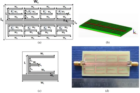
In the proposed tag, multi-resonance is achieved using cascaded E-shaped resonators excited by a 50 Ohm microstrip transmission line as shown in Figure 1(a). Each E resonator (R1–R8) of a different middle arm length introduces a different stop band resonance. The prototype is fabricated on substrate C-MET/LK4.3 by C-MET Thrissur, India with dielectric constant 4.3 and loss tangent 0.0018 [17]. Figure 1(b) shows the microstrip version of the proposed multi-resonator circuit.
(a) (b)
(c) (d)
Figure 1. (a) Layout of the proposed 8 bit multi-resonator circuit L = 10 mm, Wa = 13 mm, Wb = 12 mm, W1 = 11.8 mm, W2 = 11.5 mm, W3 = 11 mm, W4 = 10.6 mm, W5 = 10.4 mm, W6 = 9.9 mm, W7 = 9.5 mm, W8 = 8.8 mm, Wt = 59 mm, Lt = 30 mm, La = 3.5 mm, Lb = 3 mm, Lc = 1 mm, Ga = 0.5 mm, G= 1 mm, εr = 4.3, height = 1.6 mm, loss tangent 0.0018. (b) Microstrip
version of the proposed multi-resonator circuit. (c) Single E-shaped resonator. (Wj = 15 mm, Wi = 4 mm, Wk = 14 m, La = 3.5 mm, Lc = 1 mm, WL = 20 mm, L = 10 mm, Ga = 0.5 mm).
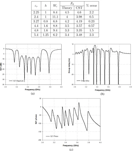
A single E-shaped resonator excited by a microstrip line as shown in Figure 1(c) is designed using CST Microwave Studio. VaryingWi,Wj and Wk results in variation in resonant frequency, bandwidth
of operating bands and Fractional Bandwidth (FBW) as illustrated in Tables 1(a), 1(b) and 1(c). The FBW is estimated using FBW = Δf/F0 ∗100%, where Δf is the 3 dB S21 bandwidth and F0 the notch frequency. The aim is to reduce the FBW to get the narrowest possible resonance at the desired frequency. From Table 1 it is clear that varying Wi by keeping Wj,Wk, L,WL and La constant gives
the lowest value of FBW. So the multi-resonator is implemented by varying the length of the middle arm (Wi).
Table 1. Variation of F0, Δf, FBW for different values ofWj,Wi and Wk.
(a) (b)
Wk =14 mm, WL= 20 mm, Wi = 14 mm, L= 10 mm,Lb = 3.5 mm.
Wj (mm) F0 (GHz) Δf (MHz) FBW (%)
8.7 2.52 200 7.93
8.2 2.54 203 7.99
7.5 2.55 218 8.54
6.3 2.57 240 9.33
5.2 2.58 257 9.96
3.5 2.59 398 15.36
Wk =14 mm,WL= 20 mm, Wj = 15 mm, L= 10 mm, Lb = 3.5 mm.
Wi (mm) F0 (GHz) Δf (MHz) FBW (%)
14 2.85 62 2.17
11.7 3.1 71 2.29
10 3.42 80 2.33
9.5 3.49 75 2.14
7 3.8 122 3.21
5.45 4.07 124 3.04
(c)
Wi =14 mm,WL= 20 mm,Wj =15 mm, L= 10 mm, Lb= 3.5 mm.
Wk (mm) F0 (GHz) Δf (MHz) FBW (%)
7.6 3.18 238 7.48
6.9 3.23 229 7.08
5.2 3.42 196 5.73
4.7 3.49 206 5.9
4.1 3.56 188 5.28
3.5 3.64 156 4.28
(a) (b)
The middle arm of the E-shaped resonator is approximately quarter wavelength long at the resonant frequency.
λg
4 =Wi+l
whereλg is the guide wavelength (λg ≈ √ελeff),lthe fringing length, andεeff the effective permittivity
of the substrate [18].
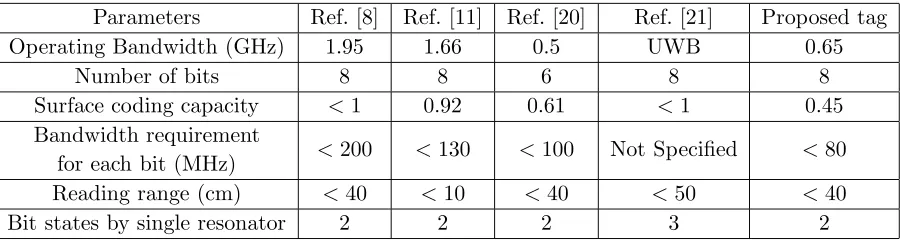
Table 2. Computed values of Wi for different resonant frequencies on various substrates.
εr h Wi F0 % error
Theory CST
2.25 1 8.4 4.5 4.6 2.2
2.4 1 11.1 4 3.98 0.5
3.27 0.8 6.8 4.2 4.19 0.23
4.4 1.6 8.8 3.5 3.57 0.57
4.8 1.6 9.4 3.3 3.35 1.5
5.4 1.25 6.2 3.4 3.48 2.3
(a) (b)
(c)
Figure 2(a) shows the variation in resonant frequency by changing Wi. It is clear that resonant frequency decreases asWi increases. This technique is used in implementing the multi-resonator circuit.
The transmission characteristics for different values of Wi are illustrated in Figure 2(b).
The middle arm length Wi can be expressed as in Eq. (1).
Wi = 2.062h−6.259F0−3.048εr+ 41.41 (1) where h is the height of the dielectric substrate in mm, εr the relative permittivity of the substrate
material, andF0 the resonant frequency in GHz. The equation is confirmed on various substrates having different values of relative permittivity and height as shown in Table 2. The equation is valid for theεr
and h in the range 2.25≤εr≤5.4; 0.8≤h≤1.6.
Figure 3 shows the simulated magnitude, phase response and group delay of the proposed multi-resonator circuit, consisting of 8 multi-resonators of varying Wi as shown in Figure 1(a). The individual resonators operate at frequencies 3.15 GHz, 3.24 GHz, 3.3 GHz, 3.38 GHz, 3.45 GHz, 3.53 GHz, 3.62 GHz and 3.77 GHz. The presence of resonance is used to encode a logic “1”, and the absence of resonance is used to encode a logic “0”. Absence of a specific resonance can be achieved, by removing the
(a)
(b) (c)
(j)
(f) (g)
(h) (i)
Figure 4. (a) Three different types of E-shaped multi-resonator. (b) SimulatedS21magnitude of Type-1 multi-resonator. (c) SimulatedS21magnitude of Type-2 multi-resonator. (d) SimulatedS21magnitude of Type-3 Multi-resonator. (e) Simulated group delay of Type-1 multi-resonator. (f) Simulated group delay of Type-2 multi-resonator. (g) Simulated group delay of Type-2 multi-resonator. (h) Simulated S21 phase of Type-1 multi-resonator. (i) Simulated S21 phase of Type-2 multi-resonator. (j) Simulated S21 phase of Type-3 multi-resonator.
3.62 3.77
3.15 3.24
3.38
3.45 3.53
3.3
Figure 5. Surface current distribution of individual resonators in the proposed multi-resonator shown in Figure 1(a).
Figure 6. Simulated transmission characteristics of the 8 bit multi-resonator. (The dimensions of the resonator are L= 10 mm, Wa = 13 mm, Wb = 12 mm, W1 = 12.2 mm, W2 = 11.7 mm, W3 = 11.2 mm, W4= 10.7 mm, W5 = 10.2 mm, W6 = 9.7 mm, W7 = 9.2 mm, W8 = 8.7 mm,Wt= 59 mm, Lt= 30 mm, La= 3.5 mm,Lb = 3 mm,Lc = 1 mmGa= 0.5 mm,G= 1 mm,εr = 4.3, height = 1.6 mm, loss tangent
(3.53 GHz) is absent. Figures 4(b)–(j) show the simulated S21, phase and group delay of the three types of resonators. The small shift in resonant frequency is due to the mutual coupling between the resonators. The absence of a specific resonator will result in a retransmitted signal with a minimum attenuation at that particular frequency. So a tag with N resonators can encode 2Nbit combinations.
Figure 5 shows surface current distributions for individual resonators, in the proposed multi-resonating circuit, at different resonant frequencies. The design has a unique feature that another set of resonant frequencies can be derived from the same structure by choosing a different set of values forWiwith all other parameters remaining the same as in Figure 1(a). The individual resonators operate
at frequencies 3.21 GHz, 3.30 GHz, 3.39 GHz, 3.48 GHz, 3.56 GHz, 3.66 GHz, 3.75 GHz and 3.86 GHz as illustrated in Figure 6. This feature provides the designer a greater advantage of designing variety of RFID tags with minimal layout modifications.
3. EXPERIMENTAL RESULTS
The measured and simulated responses of the multi-resonator for bit combination 1111 1111 are shown in Figure 7(a). Measured S21 phase and group delay response for the same bit combination are shown in Figure 7(b). Measured response of the multi-resonator for the bit combination 0110 1101 is as shown in Figure 7(c). From the figures, it is clear that either the amplitude, phase or group delay information can be used to decode the tag identity. The design parameters of the high frequency resolution multi-resonator have been chosen in order to obtain a frequency bandwidth as narrow as possible, so as to encode 8 bits in a frequency band of 650 MHz. The eight bits are represented by eight resonant nulls, which are separated approximately by 100 MHz starting from 3.12 to 3.77 GHz.
(a) (b)
(c)
4. BISTATIC MEASUREMENT SETUP
In order to improve the readability of the multi-resonator, transmitting and receiving antennas are used. Figure 8(a) shows the geometry of a circular broadband monopole antenna [19] used for the purpose. The simulated response of the antenna in the operating band of the tag is shown in Figure 8(b). The antenna operates in the range of 1.9 GHz to 4.5 GHz. The final structure of the tag thus consists of a vertically polarized circular monopole receiving antenna, an eight element multi-resonating E-structure, and a horizontally polarized circular monopole transmitting antenna. The need of two cross-polarized antennas is to minimize the interference between the transmitted signal and the retransmitted encoded signal which contains the spectral signature.
The block schematic of the measurement setup for bistatic measurement is shown in Figure 9(a). The experimental set up is shown in Figure 9(b). The tag is placed about 40 cm away from horn antennas. Two Linearly polarized medium gain (10 dB) horn antennas are used for transmission of the CW interrogation signal in the range 2–5 GHz and reception of the retransmitted signal.
The total path loss to the chipless RFID tag and back in a loss less environment can be calculated using the Friis transmission formula [3, 20]. The power density of the signal that reaches the chipless
(a) (b)
Figure 8. (a) Circular broadband monopole antenna R = 15 mm, W3 = 3 mm, Lg = 0.6 mm, Wg1 = 40 mm and Lg1 = 20 mm εr = 4.3, height = 1.6 mm. (b) Simulated reflection characteristics of antenna in Figure 8(a).
(a) (b)
RFID tag in free space is given by
St= Pt Gt
4πr2
where Pt is the transmitted power and Gt the gain of the reader transmitting antenna. The power collected by the tag’s antenna is defined as
Pa=StAet =Stλ
2
4πGtag
(a) (b)
(c) (d)
(e) (f)
Table 3. Performance comparison of different chipless RFID tag.
Parameters Ref. [8] Ref. [11] Ref. [20] Ref. [21] Proposed tag
Operating Bandwidth (GHz) 1.95 1.66 0.5 UWB 0.65
Number of bits 8 8 6 8 8
Surface coding capacity <1 0.92 0.61 <1 0.45
Bandwidth requirement
for each bit (MHz) <200 <130 <100 Not Specified <80
Reading range (cm) <40 <10 <40 <50 <40
Bit states by single resonator 2 2 2 3 2
whereAet is the effective aperture of the tag antenna,Gtag is tag’s antenna gain andλis the wavelength.
Power density of the signal that reaches the RFID reader antenna in free space is
Sr = PaGtag 4πr2
Hence, the signal received by the reader after interrogating the chipless RFID tag is defined as
Prx =SrAer = PtG 2
tagG2tλ4L
(4πr)4
where Aer is the effective aperture of the reader antenna and L the loss due to tag’s multiresonating circuit and the cross polarisation effect of antenna.
Magnitude and Group Delay studies are carried out using PNA E8362B for various bit combinations. Measured bistatic response of the RFID tag for various bit combinations are shown in Figure 10. From the figures it is evident that spectral signature is embedded inS21magnitude, phase and group delay.
Table 3 gives a comparison of the proposed chipless RFID tags with other reported tag designs. From the table it can be seen that the proposed tag requires the least operating bandwidth to encode 8 bits. Also the Bandwidth requirement to encode each bit is also less compared to other proposed designs.
5. CONCLUSION
In this paper a compact chipless RFID tag using E-shaped resonators is presented. Multiple bit encoding is possible by varyingWi of the fundamental E-structure of the proposed tag. The tag enables data encoding of 8-bits in a narrow band of 650 MHz extending from 3.12 to 3.77 GHz. The unique design feature enables the development of variety of RFID tags operating in different frequency bands. Orthogonally polarized circular monopole antenna is employed for transmission and reception purpose to reduce interference. The concept is validated from the measurements using bistatic approach for an 8-bit prototype when interrogated by a continuous wave in the frequency range of 2–5 GHz. The tag can encode data in magnitude, phase as well as in group delay.
ACKNOWLEDGMENT
The authors gratefully acknowledge Dr. R. Ratheesh Scientist, C-MET, Trichur for providing the research support.
REFERENCES
1. Finkenzeller, K.,RFID Handbook, 2nd edition, Wiley, Munich, Germany, 2003.
3. Jalaly, I. and D. Robertson, “Capacitively-tuned split microstrip resonators for RFID barcodes,” Eur. Microw. Conf., Vol. 2, 4–7, Paris, France, Oct. 4–6, 2005.
4. Tikhov, Y. and Y. H. Min, “RFID barcode and RFID barcode reading system,” Patent No. US20070164121, Jul. 19, 2007.
5. McVay, J., A. Hoorfar, and N. Engheta, “Theory and experiments on Peano and Hilbert curve RFID tags,” Proc. SPIE, Vol. 6248, No. 1, 624808-1–624808-10, 2006.
6. Balbin, I., S. Preradovic, N. C. Karmakar, and G. F. Swiegers, “Multi-resonator-based chipless RFID system for low-cost item tracking,” IEEE Trans. Microwave Theory Tech., Vol. 57, 1411– 1419, 2009.
7. Jang, H.-S., W.-G. Lim, K.-S. Oh, S.-M. Moon, and J.-W. Yu, “Design of low-cost chipless system using printable chipless tag with electromagnetic code,” IEEE Microw. Wirel. Components Lett., Vol. 20, No. 11, 640–642, 2010.
8. Nijas, C. M., R. Dinesh, U. Deepak, A. Rasheed, S. Mridula, K. Vasudevan, and P. Mohanan, “Chipless RFID tag using multiple microstrip open stub resonators,” IEEE Trans. Antennas Propag., Vol. 60, No. 9, 4429–4432, 2012.
9. Kalansuriya, P., N. C. Karmakar, and E. Viterbo, “On the detection of frequency-spectra-based chipless RFID using UWB impulsed interrogation,”IEEE Trans. Microwave Theory Tech., Vol. 60, No. 12, 4187–4197, 2013.
10. Sumi, M., C. M. Nijas, R. Dinesh, and S. Mridula, “Chipless RFID tag based on spurline resonators,” Proceedings of National Symposium on Microwave Antennas and Propagation, 165– 168, Cochin, 2012.
11. Sumi, M., R. Dinesh, C. M. Nijas, S. Mridula, and P. Mohanan, “Frequency coded chipless RFID tag using spurline resonators,” Radio Eng., Vol. 24, No. 4, 203–208, 2014.
12. Casula, G. A., G. Montisci, P. Maxia, and G. A. Mazzarella, “A narrowband chipless multiresonator tag for UHF RFID,”Journal of Electromagnetic Waves and Applications, Vol. 28, No. 2, 214–227, 2014.
13. Vena, A., E. Perret, and S. Tedjini, “High capacity chipless RFID tag insensitive to the polarization,” IEEE Trans. Antennas Propag., Vol. 60, No. 10, 4509–4515, 2012.
14. Islam, M. A., Y. Yap, N. Karmakar, and A. K. M. Azad, “Orientation independent compact chipless RFID tag,”IEEE 2012 International Conference on RFID-Technologies and Applications, 137–141, Nov. 5–7, 2012.
15. Nair, R. S., E. Perret, S. Tedjini, and T. Baron, “A group-delay-based chipless RFID humidity tag sensor using silicon nanowires,” IEEE Antennas Wireless Propagation Letters, Vol. 12, 729–732, 2013.
16. Nijas, C. M., U. Deepak, P. V. Vinesh, R. Sujith, S. Mridula, K. Vasudevan, and P. Mohanan, “Low-cost multiple-bit encoded chipless RFID tag using stepped impedance resonator,” IEEE Trans. Antennas Propag., Vol. 62, No. 9, 4762–4770, Sep. 2014.
17. Ratheesh, R., K. S. Jacob, K. P. Murali, A. Jain, and P. R. Hannurkar “Ceramic filler, method of preparing ceramic filler and applications as resonator and laminate thereof,” US Patent 14228342, Mar. 2014.
18. Bahl, I. J. and P. Bhartia, Microstrip Antennas, Artech House, Norwood, MA, 1980.
19. Preradovic, S., I. Balbin, N. C. Karmakar, and G. Swiegers, “A novel chipless RFID system based on planar multi-resonators for barcode replacement,”Proceedings of IEEE International Conference on RFID, 289–296, Las Vegas, 2008.
20. Karmakar, N. C. and G. F. Swiegers, “Multiresonator-based chipless RFID system for low-cost item tracking,” IEEE Trans. Microwave Theory Tech., Vol. 57, No. 5, 1411–1419, May 2009. 21. Girbau, D., J. Lorenzo, A. L´azaro, C. Ferrater, and R. Villarino, “Frequency-coded chipless RFID