Noise Reduction Technique In A Fully
Differential Difference Amplifier Using G
m
/I
d
Rishi Todani and Ashis Kumar Mal
Abstract: This paper presents a noise reduction technique while designing a fully differential difference amplifier using gm/ID method. It provides an easy technique to alter the corner frequency of noise and also exhibit a good matching between analytical and simulated results for unity gain bandwidth, even in sub-micron technology. Stability, noise, PVT and Monte Carlo analysis validate the designed circuit. The amplifier is designed using SCL 180nm CMOS technology and 1.8V supply.
Index Terms: gm/Id method, Low Input Referred Noise, Fully Differential Difference Amplifier (FDDA).
—————————— ——————————
1.
INTRODUCTION
A fully differential difference amplifier (FDDA) has become a popular choice among analog designers. It provides low output distortion and high voltage swing as compared to a single ended differential difference amplifier (DDA). Analog circuits designed using FDDA possess attractive features which do not exist in circuits built using traditional and modern opamp circuits. Various noise reduction techniques are available in literature and are also being studied worldwide. Techniques include both, architecture optimization and appropriate device sizing method. In this paper we resort to the latter, appropriate device sizing for low noise. A classical CMOS design is based on square law equation that represent the basic MOS model. However with modern technology square law equation fails to replicate the behavior of the deep sub-micron (DSM) devices. Various alternate methods like geometric programming [2], [3], gm/ID method [4], [5] and potential distribution method [6] have also been put forward. In this paper we focus on one of the solutions, gm/ID method, a parameter provided by BSIM model.
2
FDDA
ARCHITECTURE
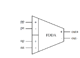
FDDA [7] block diagram is shown in Fig. 1. It consists of two sets of differential input pair which provide high input swing and a common mode feedback (CMFB) circuit. The latter enables a stable output common mode level. For better results, gain of the CMFB path must be high.
Fig. 1. Fully differential difference amplifier
3 NOISE
ANALYSIS
IN
AMPLIFIER
Input referred noise [10] indicates the level of distortion or corruption in the input signal due to the noise present in the circuit. Dominantly, two types of noise are present in MOS device:
3.1 Thermal Noise
Thermal noise [10] is generated inside the gate channel. It can be modeled as a voltage source power spectral density shown in equation (1).
̂
(1)
where, coefficient γ is 2/3 for long channel and increases as channel length decreases. As a rule of thumb we assume γ = 1 [10]. Other symbols have their usual meaning.
3.2 Flicker Noise
Flicker Noise [10] arises at the interface between the gate oxide layer and silicon substrate in a MOSFET. It is due to the dangling bond present between the oxide and the silicon substrate. As carriers move near the interface, some are randomly trapped and later released with some energy states that introduce flicker noise. Flicker Noise equation is shown in equation (2).
̂
(2)
Where, Kf is process dependent constant of the order 10-25V2F. This expression assumes a bandwidth of 1 Hz. Corner Frequency fcorner is a frequency where the thermal noise source is equal to flicker noise source, given in equation (3).
————————————————
Rishi Todani obtained is currently working as a Project Faculty in SMDP C2SD program in ECE Department at NIT Durgapur. E-mail: [email protected]
Tusha Tanya is currently working as Research associate at IIT Delhi and finished her M. Tech. from NIT Durgapur in 2019.
Fig. 2 : Folded Casode FDDA
(3)
Before going directly to the design step, it is necessary to know which transistors dominate the input referred noise in folded cascode fully differential difference amplifier. For MOSFETs input referred noise [11] is a combined power spectral density of both thermal and flicker noise. Total output Noise [12] present in the circuit Fig. 2 is shown in equation (4) to equation (6). Most Noise is contributed by the transistors M11, M12, M05, M06 and differential input pairs M01 - M02, M03 - M04.
̂ [ ( )
( ) ] (4)
̂ [ ( )
( )
( ) ] (5)
̂ [ ( )
( ) ( ) ] (6)
Input referred noise per unit bandwidth is equal to the total noise present at the output divided by square of the gain of the amplifier shown in equation 7.
̂ ̂ ̂ ̂ ( ) (7)
where Rout is output resistance of the fully differential difference amplifier given in equation 8.
{ } { ( )} (8)
4
DESIGN
ALGORITHM
gm/ID method [4], [5] is used to find the width of the differential input pairs by following design flow presented in Fig. 3.
Fig. 3. Device sizing algorithm
Assume slew rate is 1 V/μs, thus Itail can be calculated as
(9)
For Unity Gain Bandwidth of 1MHz trans-conductance is calculated as
(10)
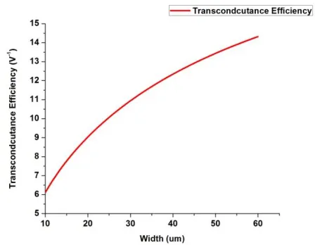
Plot of gm/ID Vs. width of input differential pair using standard CMOS technology is shown in Fig. 4.
Fig. 4. gm/ID vs differential input pair width
Dimensions of M01-M04 differential input pairs are obtained from Fig. 4 using the principle depicted in Fig. 3. First, gm and ID are estimated as per equations (9) and (10), and gm/ID is evaluated. The width of device is then read from Fig. 4. Sizing of transistors M11 and M12 are done using gm/ID for low noise. Equation 3 can be re-written as:
(11)
5
SIMULATION
RESULTS
Detailed simulations are carried out and the results are tabulated along with target specifications in Table I. The table shows good noise characteristics at 1 kHz. Sampling a low frequency signal at around 1 MHz, where noise below 50 nV/ H is desirable. Detailed results are discussed ahead.
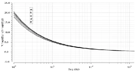
5.1 Stability and Noise
Bode plot of the designed structure is shown in Fig. 5 and input noise is depicted in Fig. 6. The results of the same are summarized in Table I. Transient characteristics like slew rate of 1V/μs. The results obtained are also compared with earlier published literature. The power indicated in the table includes the power consumed by the CMFB and the current reference generating circuit along with the main opamp section.
Fig. 5. Stability analysis pre layout
5.2 Noise Corner Analysis
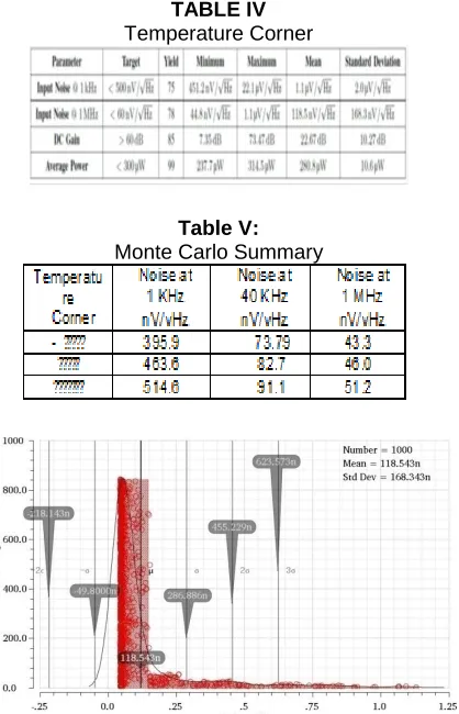
Process variation effect on input noise is simulated at the five corners and is shown in Fig. 7 and summarized in Table II. In all the five corners, noise is seen to be below the desired level. This proves the validity of the design under process variations. Supply voltage corner with 10% variation in VDD is simulated and variation in input noise is shown in Fig. 8 and Table III. Negligible variation in noise measurements is seen. Temperature corners of - 0 and 100 are performed showing satisfactory results in Fig. 9 and Table IV.
Table I : Simulation Results
Fig. 6. Input noise pre layout
5.3 Monte Carlo Analysis
Monte Carlo analysis for process and mismatch combined simultaneously is run for 1000 samples. Gaussian distribution was employed in the simulation. Measurement of noise at 1 kHz and 1 MHz along with DC gain and power was carried out. The histograms are shown in Fig. 10 through Fig. 14. The results of the analysis are mentioned in Table V in detail. It approves the rigidity of the design.
Fig. 7. Process corner analysis
Fig. 9. Temperature corner analysis
TABLE II Process Corner Analysis
TABLE III Supply Voltage Corner
Fig. 10. Monte Carlo analysis - Input noise at 1 kHz
Fig. 11. Monte Carlo analysis - Input noise at 40 kHz
TABLE IV Temperature Corner
Table V: Monte Carlo Summary
Fig. 12. Monte Carlo analysis - Input noise at 1 MHz
Fig. 13. Monte Carlo analysis - DC Gain
Fig. 14. Monte Carlo analysis – Power
Process
Corner nV/ H Noise at 1 KHz
nV/ H Noise at 40 KHz
nV/ H Noise at 1 MHz
tt 463.6 82.7 46.0
ff 418.5 75.0 42.4
ss 480.9 85.6 47.6
sf 438.4 78.1 43.7
fs 474.4 84.7 47.1
Voltage Corner
nV/ H Noise at 1 KHz
nV/ H Noise at 40
KHz
nV/ H Noise at 1 MHz
1.62 V 458.3 82.2 46.6
1.8 V 463.6 82.7 46.0
Fig. 15. Layout of opamp
Fig. 16. Post Layout stability analysis
6.
LAYOUT
DESIGN
After verification of pre-layout design in simulator, layout is drawn using virtuoso Layout editor. Complete layout of FDDA is shown in Fig. 15. Wide transistors are usually fingered [13] so as to reduce the S/D area as well as gate resistance. Matched transistors in layout are placed together to reduce the effect of process variation. For matched transistors, common centroid and inter-digitated method [14], [15] are used. Dummies are added to get the same environment for matched transistors. Once layout is drawn, it is verified through DRC check, Layout Vs. Schematic (LVS). Post layout simulation is carried out after parasitic extraction is done. Post layout simulation results are given in Table I and bode plot is given in Fig. 15. The results are seen to be within desired specifications.
7
CONCLUSION
This paper discusses a design technique for a low noise folded cascode based fully differential difference amplifier. It discusses a simple method to control noise and unity gain frquency of the amplifier. An input noise of 463 nV/ H at 1 kHz was obtained with an overall power consumption of 280 μW. Detailed stability, noise, PVT and Monte Carlo analysis of the circuit were carried out and results were presented. The design was carried out in SCL 180 nm CMOS technology and 1.8V supply using Cadence design tools.
8.
ACKNOWLEDGEMENT
The authors would like to acknowledge The Ministry of Electronics and Information Technology, Government of India for leading the Chip to System Design activities (SMDP-C2SD) in India. The authors are also thankful to Prof. Pradip Mandal and Prof. Anindya Sundar Dhar of Electrical and EC Engineering Dept., IIT Kharagpur, and Dr. Rajat Mahapatra of Department of ECE at NIT Durgapur for their kind support throughout the project.
9.
REFERENCES
[1] Kai-Wen Yao, Wei-Chih Lin, Cihun-Siyong Alex Gong, Yu-Ying Lin and Muh-Tian Shiue, ‖A differential difference amplifier for neural recording system with tunable low-frequency cutoff,‖ 2008 IEEE International Conference on Electron Devices and Solid-State Circuits, Hong Kong, 2008, pp. 1-4.
[2] M. d. Hershenson, S. P. Boyd and T. H. Lee, ―Optimal design of a CMOS op-amp via geometric programming,‖ in IEEE Transactions on Computer-Aided Design of Integrated Circuits and Systems, vol. 20, no. 1, pp. 1-21, Jan 2001.
[3] P. Mandal and V. Visvanathan, ―CMOS Op. Amp Si ing using a Geometric Programming Formulation,‖ in IEEE Transactions on Computer-Aided Design of Integrated Circuits and Systems, vol. 20, no. 1, pp 22 - 38, 2001.
[4] P. Jespers, ―The gm/ID Methodology, a sizing tool for low-voltage analog CMOS circuits,‖ Springer, 2009. [5] F. Silveira , D.Flandre and P. Jespers, ―A gm=ID
Based Methodology for the Design of CMOS Analog Circuits and Its Application to the Synthesis of a Silicon-on-Insulator Micropower OTA,‖ IEEE Journal of Solid-State Circuits, Vol. 31, No. 9, September 1996.
[6] Rishi Todani and Ashis Kumar Mal, ―Simulator Based Device Si ing Technique for Operational Amplifiers,‖ WSEAS Transactions on Circuits and Systems, Volume 13, Art. 2, pp.11-28, 2014.
[7] Eduard Sackinger, and Walter Guggenbuhl, ―A Versatile Building Block: The CMOS Differential difference Amplifier, ‖IEEE Journal of solid-state circuits, vol.sc-22, No.2, April 1987.
[8] D. Jana and A. K. Mal, ‖Design of low noise amplifier for sensor applications,‖ 2017 Devices for Integrated Circuit (DevIC), Kalyani, pp. 451-455, 2017.
[9] J. Baker, ―CMOS Design, Layout and Simulation, ‖Wiley – IEEE Press, 2005.
[10] Beh ad Ra avi, ―Design of Analog CMOS Integrated Circuits, ‖McGraw-Hill International edition, 2005. [11] Meysam Akbari, Sadegh Biabanifard and Shahroz
Asadi,―Input Referred Noise Reduction Technique for Transconductance Amplifiers,‖ Electrical & Computer Engineering: An International Journal (ECIJ), Vol. 4, No.4, December 2015.
[12] R. Reid and Cameron Charles,―A Low-Power Low Noise CMOS Amplifier for Neural Recording Applications,‖ IEEE Journal of Solid-State Circuits, Vol.38, No. 6, June 2003.
Solid-State Circuits, Vol. 38, No. 3, pp. 450-456, March 2003.
[14] Christopher Saint and Judy Saint, ―IC Layout Basics A Practical Guide,‖ McGraw-Hill,2002. J. D. Bruce,