ISSN
1029-3221
EAST AFRICAN
JOURNAL OF
SCIENCE
EDXRF analysis of local and imported pica soil samples.
E.N.M. Njagi, A.M. Kinyua, J.K. Munyua & M.J. Mangala.
19
I
Volume 3 - Part 1 June202iJ
Contents
The occurrence of larval Contracaecum sp. (Nematoda: Heterocheilidae) in three teleostean fish species from Lake Naivasha, Kenya.
P.A. Aloo. 1
Population level of bean rhizobia in the soil of semi-arid south-east Kenya and assessment of symbiotic behaviour.
J.M. Maingi, C.A. Shisanya, N.M. Gitonga &B. Hometz.
13
Linear and non-linear optical properties of amorphous Si.
J. Okumu
&
G.J. Morgan. 25Computation of electronic properties of amorphous silicon (a-Si).
Y.M. Wambua, J. Okumu & T.S. Dod. 35
Electrical conductivity in doped polymers.
D.B. Bern 43
Calculation of linear and non-linear optical properties of amorphous
Silicon
. J. Okumu' and G. J. Morgan2.. .
'Department of Physics, Kenyatta University, P.O. Box 43844, Nairobi, Kenya. .
2Department of Physics and Astronomy, The E.C Stoner Building, University of Leeds, Leeds LS2 9JT, UK.·
We have used the random phase model for the electronic wave functions to calculate the imaginary part of the dielectric function 82(m) and the magnitude of the third harmonic
generation,
11'3
(OJ ~ using a model structure of a-Si containing 1728 atoms. We show that thissimple calculation gives reasonable results for e(e) and furthermore the behaviour of ..
l
«(l).issimilar to more detailed theoretical calculations.
Keywords: disordered systems; semiconductors; optical properties
(.> "
INTRODUCTION
The study of optical properties of solids has proved to be a powerful tool in the understanding of· the electronic and atomic structure of solids. A number of techniques have been developed to calculate the linear optical properties of semiconducting materials but the situation is different for non-linear optical spectra. The non-linear response is of interest from an application point of view but also as a means of characterising surface properties. The calculation of the response function
l(ro)
is a time consuming business even in crystals (Mosset al.,
1990; Ching & Huang, 1993). The number of full band structure calculations for the third non-linear susceptibility tensori(3)(m) is extremely small. This is because of the general complexity of the third order non-linear optical processes even for the simplest of crystals. The work of Moss
et al
.
(1990) using both an empirical tight-binding and semi ab-initio band structure technique and that of Ching and Huang (1993) using the first principles orthogonalised linear combination of atomic orbitals method for a series of group III-IV semiconductors are the first band structure calculations ofx(3)(m). Experimental data are very scarce, with. measurements often made at only one frequency. Where experimental data exist, for example of x(3)(m) at zero frequency for these group III-IV crystalline semiconductors, it is gratifying. that there is good agreement between
these predictions and measurements. I
The methods that exist for the calculation of optical properties of crystalline semiconductors especially the non-linear optical spectra exploit the periodicity of the crystal lattice. In amorphous semiconductors with no long-range order and where large structural models are required, calculations are much more difficult. Calculations or experimental measurements are almost non-existent for amorphous semiconductors.
26 - Okumu & Morgan, Optical properties of amorphous silicon
paper is to show that a simple calculation using a model structure can be used to make very reasonable estimates of'1:(ro).
We also make some comments on the behaviour of l(ro) at low frequencies. The work of Hobbs
et al.
(1996) was based on expressions given by Mosset al.
(1990) and we also make use of these particular forms.THEORY AND COMPUTATIONAL
DETAILS
If the particular wave functions in a solid are written in terms oflocalised atomic-like orbitals
If/(r) ~ LalllmU);lIIm(r -~) 11Im
••..••.•...•••...•..••.••...•.••
(1)corresponding to orbitals labelled by
nlm
on a siterj
then the random phase. type of approximation assumes that the amplitudes of the orbitals can be 'approximated' by the form (Mott, 1967; Friedman, 1971) .anlmU)
=
N
-
1/2 a~/mexp(i(}lIIm(j») •••••••••••••••••••••••••••••• (2)where ()lIIm(j) is a random phase varying with the value of
nlm
and j, andN
is the number of atoms in the solid. This assumed form cannot, of course, be true in the sense that the wave functions must satisfy Schrodinger's equation but it doesisolate terms in expressions for the. response formulae that are positive definite and the hope is then that any other terms will tend to cancel out. The degree to which this is justified can be seen in calculation of say the conductivity by Okumu
et al.
(1995) in a -Si where very reasonable agreement is obtained with the computed behaviour for the conductivity asa
function of energy.The simplest way in which equation (2) may be employed is to take a~m to be-unity, which implies that at each energy level each orbital contributes equally to the density of states. Expressions for response coefficients then involve integrals over the electronic densities. Matrix elements of, say, the momentum operator can be evaluated for a particular structure within this approximation or the matrix elements may be treated as constants and determined empirically.
. We in fact will follow both routes in this work.
A refinement that was employed by Okumu
et al.
(1995) is to writeo
a.;>
...
~••.••...•...
(3).
whereg
(E)
is the partial density of states associated with the orbital labelled bynlm
and111m
glllm(E) is the average density of states over the energy range described by the localised orbitals. Yet a further refmement would be to take advantage of any knowledge of the local density of
Let us first considerthe behaviour of the imaginary part of the dielectric function where (Connell, 1976)
s(
w)
= ~ (
27reJ
'
I.I
f1(tI~i)1
zJ(Ef - E.-/i",)
(4)mm
.
where Qis the volume of the system, i and f denote the initial and final states when a photon "of energy ~w is absorbed, p is a component of the momentum operator. The final states must be\
unoccupied and the initial states occupied. If the matrix elements are treated as constants then 82(W) can be written as
3 2 .
Zne 2 a Pcv "
&2(w)=2(-) --L...0(Ej -E; -liw)
mai Q if
(5)
gcor vdenotes the density of states/spin/unit volume in the conduction band or valence band and is just a length of the order of the atomic spacing.
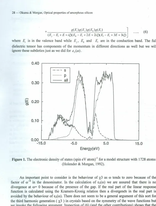
Calculations for both linear and non-linear optical spectra are performed on a model structure of silicon containing 1728 atoms (Holender & Morgan, 1991). The structure is generated using molecular dynamics starting from an amorphous model of 216 atoms and putting together a number of these blocks. This structure has about 4% over co-ordinated and 2% under co-ordinated atoms leading to gap states in the density of states shown in Figure 1 (Holender &
.Morgan, 1992). It is extremely difficult to generate large models without states being produced in the gap by under and over co-ordinated sites. For our present purpose we have removed the states produced by the 'defect' sites so that we create a gap ofl eV since we are interested in interband transitions. This simple device is sufficient.for our present purpose.
Moss
et al.
(1990) used perturbation theory to separateX3(00)
into three contributions termed virtual electron (VE), virtual hole .(VH) and three-state processes (3S). Only the VE processes will be detailed here to show the nature of the calculation. If we take matrix elements of the momentum as constants then the virtual electron contribution becomes+
g(E;)g(Ej)g(Ek)g(E[)(Ej - E,+E+i;)(Ek - E;+2E+2i;)(E[ - E;; - E - i;)
+
g(E;)g(E)g(Ek )g(E[)28- Okumu &Morgan, Optical properties of amorphous silicon
+
g(Ej)g(E)g(Ek)g(E,)1
(6)(Ej - E,+E +i~(Ek - E, +2E +2i~(E, - E,+3E +3i~
where E; is in the valence band while Ej' E, and E, are in the conduction band. The full
dielectric tensor has components of the momentum in different directions as well but we will ignore these subtleties just as we did for &2((1)) .
0
.
40
0.30
-~
0.20
C>
0.10
0.00
-15.0
a
o
s
...
.
.
...p
--
all
-5.0
5.0
15.0
Energy(eV)
Figure 1.The electronic density of states (spin eV atom)" for a model structure with 1728 atoms (Holender &Morgan, 1992).
An important point to consider is the behaviour of X) as 0) tends to zero because of the factor of 0)-4 in the denominator. In the calculation of E2( 0)) we are assured that there is no divergence at 0)= 0 because of the presence of the gap. If the real part of the linear response function is calculated using the Kramers-Kronig relation then a divergence in the real part is avoided by the behaviour of E2( 0)). There does not seem to be a general argument of this sort for the third harmonic generation ( X3 ) in crystals based on the symmetry of the wave functions but we invoke the following argument. Inspection of (6) (and the other contributions) shows that the imaginary part of X3 must vanish for EL Eg/3 where Eg is the energy gap. The real part is given
(7)
where ~ is an infinitesimal. The fact that Imx3 does not diverge implies that Rex3 is also well
behaved. What we can expect is that Rex3 will peak as
co
sweeps through the zero in Imx3 atEg/3.
The numerical integration required some care. We used a finite value of ~ =lev bearing in mind that the widths of the valence band are about 15eVeach. This produces a spurious extension of Imx3 below Eg/3. Cutting of Imx3 with a discontinuity would produce a spurious divergence in
Rex3. We therefore smooth the sharp edge by multiplying by
Sin~( E - ~g /
3)
for(E - Eg /
3) ~ 1 and unity thereafter. None of these considerations should be important as regards the general behaviour ofX
3•RESUL TS AND DISCUSSION
In figure 2 we show the behaviour of E2(a» using densities of states calculated by Holender and
Morgan for a model structure of a Si containing 1728 atoms (Holender &Morgan 1991). In figure 4 we show E2(a» fitted to the experimental results of Pierce and Spicer (1972) at an energy of
3eV and corresponds to choosing a3
p;v
=
20.6au. The peak position is around 5eV whereas theexperimental results peak near 3.5eV ( Figure 3). If we evaluate E2(a» using the simple r.p.m.
then the shape will be identical to that produced by Eq. (5) but the matrix elements are now calculated using parameters for s and p-type tight binding hopping integrals of Chadi (1984). The r.p.m. yields a lower peak value than experiment and seems also to be a feature of more elaborate ,
calculations, Weaire et al. (1991, 1993). Increasing the gap would push the calculated position of '
the peak to higher energies. This discussion of E2(a» is a precursor to evaluating
X3(CO)
becausewe will use the value a3p~
=
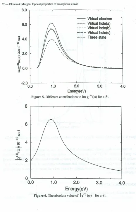
20.6au in those calculations.In figures 5 and 6 we show the different contributions to Imx3 and the total value of
I
XI
3.The fact that all processes seem to make comparable contributions (see figure 5) has been noted by Ching and Huang (1993). The magnitude and form of X3is similar to that calculated by Hobbs
et al. (1996) on a small structure of216 atoms though the equation-of-motion method can lead
I
o
rather noisy results for small models and we have eliminated spurious divergences as described above.
In Fig. 6 the absolute value
Ii
(3)(m)1
is given which is to be compared with othertheoretical predictions of Moss et
al.
(1990) for crystalline silicon since there are no previous calculations ofli(3)
(w)1 for a-Si. More recent calculations by Ching and Huang (1993) using first30 - Okumu &Morgan, Optical properties of amorphous silicon
10.0
Energy(eV)
Figure 2. The imaginary part of the dielectric constant E2((J) in the rpm for a-Si,
10.0
Energy(eV)
Figure 3. The imaginary part of the dielectric constant E2((J) calculated from Matrix elements
extracted from experimental measurements for a-Si.
20.0
15.0
-~ 10.0
C/J
5.0
0.0
0.0
30.0
20.0
-
S'-' ~
10.0
5.0
15.0
20.0
0.0
40 SILICON
°0~~~~~~4--L-~6~~~8~~-1~0--L-~12
PHOTON ENERGY (~VI CRYSTAL
35
...
..
"'30
z
~
en
Z o
u ~25
a:
.
..
~-'
w
a
5
Figure 4. Experimental results ofE2(o) for a-Si and crystalline silicon ( Pierce &Spicer, 1972).
In conclusion these results demonstrate that the rpm type of approximation can be used to
make good estimates of
li()}
(m)1
in amorphous solids and in future it will be worthwhileextending the calculation using partial density of p and s- states which could give finer features of
the spectra. These calculations also suggest that reasonable estimates of surface variation in
i
3may also be useful making use of local density of states and evaluation of matrix elements using the tight-binding scheme.
ACKNOWLEDGEMENTS
,
32 - Okumu & Morgan, Optical properties of amorphous silicon
-
~ 4.0
Q
'6
-
X\0
~ 2.0
--a
-•....
<"'I
i
0.0
6
-
:::t~
0
-
I4
0
-'-'
~
a
'-'
-('f"I
-~
2
8.0
~--~--~----~---r--~----~--~--~
6.0
--
Virtual electron
._.._.... Virtual hole(a)
- - - - Virtual hole(b)
- - - Virtual hole(c)
- - -
Three state
----2.0 '
-
...
J
-
__
.;...--I ...L...-__ --'-- __--
1
__
.
"
"-
----
l
0.0
1.0
2.0
3.0
4.0
Energy(eV)
Figure 5. Different contributions to Im X3)(ill) for a-Si.
8
o
0.0
1.0
2.0
3.0
4.0
Energy(eV)
References
Chadi, D.J. 1984. Theoretical study of the atomic structure of silicon (211), (311), and (331) surfaces. Physical Review B 29: 785-792.
Ching, W.Y. & Huang, M.-Z. 1993. Calculation of optical excitations in cubic semiconductors.
III.Third-harmonic generation. Physical Review B 47: 9479-9491.
Connell, G.A.N. 1976. Optical properties in amorphous semiconductors. In: M.H. Brodsky (ed.),
Topics in Applied Physics, Vol. 26, Springer, Berlin.
Friedman, L. 1971. Hall conductivity of amorphous semiconductors in the random phase model.
Journal of Non-Crystalline Solids 6: 329-341.
Hobbs, D.,Weaire, D., McMurry, S. & Zuchnat, O. 1996. The computation of linear and non
-linear optical constants of semiconductors. Journal of Physics: Condensed Matter 8: 4691
-4
-
1Q4.
Helender, J.M. & Morgan, G.J. 1991. Molecular dynamics simulation of a large structure of amorphous Si and direct calculation of the structure factor. Journal of Physics: Condensed Matter 3: 1747-1952.
Holender, J.M. & Morgan, GJ. 1992. The electronic structure and conductivity of large models of amorphous silicon. Journal of Physics: Condensed Matter 4: 4473-4482.
Holender, J.M. & Morgan, G.J. 1994. Electron localization in models ofhydrogenated amorphous silicon and pure amorphous silicon. Modelling and simulation of Materials in Science and Engineering 2: 1-8.
Moss, D.J., Ghahramani, E., Sipe, J.E. & Van Driel, H.M. 1990. Band-structure calculation of dispersion and anisotropy in i(3) for third-harmonic generation in Si, Ge, and GaAs. Physical
Review B 41: 1542-1560.
Mott, N.F. 1967. Electrons in disordered structures. Advances in Physics 16:49-97.
Okumu, J., Holender, J.M. & Morgan, G.1. 1995. The Hall effect and electronic conduction in amorphous Si.Philosophical Magazine Letters 72: 135-142.
Pierce, D.T. & Spicer, W.E. 1972. Electronic structure of amorphous Si. Physical Review B 5:
3017-3036.
Weaire, D., Hickey, BJ. & Morgan, GJ. 1991. Application of the equation-of-motion method to the calculation of optical properties. Journal of Physics: Condense Matter 3: 9575-9578. Weaire, D., Hobbs, D., Morgan, G.J., Holender, J.M. & Wooten, F. 1993. New applications of
the equation-of-motion method: optical properties. Journal of Non-Crystalline Solids