University of South Carolina
Scholar Commons
Theses and Dissertations
2017
Geometric Influence on Electronic Properties:
Graphene with Antidots, Two-Dimensional
Electron Gas and Three-Dimensional Carbon
Nanostructures
Lei Wang
University of South Carolina
Follow this and additional works at:https://scholarcommons.sc.edu/etd
Part of thePhysics Commons
This Open Access Dissertation is brought to you by Scholar Commons. It has been accepted for inclusion in Theses and Dissertations by an authorized administrator of Scholar Commons. For more information, please [email protected].
Recommended Citation
G
EOMETRICI
NFLUENCE ONE
LECTRONICP
ROPERTIES:
G
RAPHENE WITHA
NTIDOTS,
T
WO-D
IMENSIONALE
LECTRONG
AS ANDT
HREE-D
IMENSIONALC
ARBONN
ANOSTRUCTURESby
Lei Wang
Bachelor of Science
Shandong University of Science and Technology, 2008
Master of Science
Chinese Academy of Sciences, 2011
Submitted in Partial Fulfillment of the Requirements
For the Degree of Doctor of Philosophy in
Physics
College of Arts and Sciences
University of South Carolina
2017
Accepted by:
Timir Datta, Major Professor
Richard Creswick, Committee Member
Milind Kunchur, Committee Member
Richard Adams, Committee Member
Ming Yin, Committee Member
DEDICATION
ACKNOWLEDGEMENTS
First, I want to thank my advisor Dr. Timir Datta for his endless support and help on
my study and life. Dr. Datta is always full of patience, energy and wisdom. He keeps
reminding me to be creative. I can always learn new things when we discuss the
experiment and data. My written English has been improved a lot and I learned how to
express myself clearly during manuscript revision. Furthermore, he cares about my life,
just like my daddy. We went to beach together to enjoy the break. He told me how to get
along with people and assimilate into American culture, how to deal with trouble in life.
Second, I started the cooperation with Dr. Ming Yin since 2012. We traveled to
National High Magnetic Field Laboratory several times together with his funding. He is
always glad to help me to set up the equipment, fill the helium and take data. I really
enjoy the collaboration with him. I cannot finish my thesis without his generous support.
Third, I would love to thank my committee members. Dr. Richard Creswick as
graduate director gave me a lot of help for the recommendation letters and application for
travel grants of Graduate School. I really appreciate his careful revision and constructive
suggestions on my PhD thesis. The thin film course offered by Dr. Milind Kunchur is
very useful for my research. Really appreciate Dr. Richard Adams from Chemistry
Then, special thanks go to Dr. Richard Webb, Dr. Thomas Crawford, Dr. Bochen
Zhong, Ning Lu and Heath Smith for the help of graphene nanostructure fabrication.
Thank Dr. Asif Khan, Sakib Muhtadi, Dr. Fatima Asif and Antown Coleman in Electrical
Engineering Department for the help of AlInN/GaN device fabrication.
I got a lot of help from Dr. Jan Jaroszynski, Dr. Eun Sang Choi and Dr. Ju-Hyun Park
when I conducted measurements at the National High Magnetic field Laboratory,
Tallahassee FL. I really appreciate your assistance and useful discussion.
To my best friend, Dr. Dawei Li, we experienced a lot. To Katia Gasperi, Nahid
Shayesteh Moghaddam, Lin Li, Tongtong Cao and Hao Jiang, you guys are awesome and
I don’t think I could make it without your help and encouragement.
Finally, my family is a constant power source for my growth and accomplishment of
ABSTRACT
Geometric influence on electrical and magneto transport properties has been
investigated in three types of systems: (i) Graphene, a single layer of carbon atoms; (ii)
Two-dimensional electron gas (2DEG) in AlInN/GaN heterostructure; and (iii) 3D carbon
nanostructures, a special type of three-dimensional materials with spherical voids. Due to
unique structures and energy dispersion relations, these three systems demonstrate
distinct physical properties.
AlInN is the newest and amongst the widest band gap semiconductors. The 2DEG in
AlInN/GaN heterostucture displays long transport lifetime along with conventional
behaviors, including Shubnikov-de Haas (SdH) oscillation and weak localization. From
SdH oscillation, the effective mass of electron is obtained as 0.2327me. We report the
first observation of weak localization in this heterostructure. Electron-electron scattering
is the principal phase breaking mechanism in this system.
In contrast, graphene has an unconventional linear energy dispersion relation near the
Dirac points. We determine the effective mass of electron is 0.087me in CVD graphene,
much smaller than that in 2DEG. In addition, due to pseudo spin and nonzero Berry
phase, weak localization in graphene is more complex. Furthermore, the introduction of
an antidot lattice has great influence on transport in graphene. We demonstrate that the
antidot size, a band gap ~ 10 meV is obtained. Geometric control of the band gap is likely
to promote electronic applications of graphene.
As observed in graphene and the 2DEG, the magneto response is typically sensitive to
the orientation between the applied magnetic field and input current. However, we
demonstrate that orientation independent response and linear magnetoresistance can be
achieved in three-dimensional carbon nanostructures with spherical voids. With the
increasing void size, the linear magnetoresistance is enhanced and a metal to insulator
transition is observed. The combination of orientation insensitivity and linear
magnetoresistance is very useful for magnetic field detectors, particularly at high
TABLE OF CONTENTS
Dedication ... iii
Acknowledgements ... iv
Abstract ... vi
List of Tables ...x
List of Figures ... xi
List of Symbols ...xv
List of Abbreviations ... xvii
Chapter 1 INTRODUCTION ...1
1.1 Transport theory ...3
1.2 AlInN/GaN heterostructure ...8
1.3 Landau level and Shubnikov-de Haas oscillation ...12
1.4 Graphene ...15
1.5 Weak localization...19
Chapter 2 DEVICE FABRICATION AND TRANSPORT MEASUREMENT ...25
2.1 Fabrication and characterization of Graphene with antidots ...25
2.2 Fabrication of AlInN/GaN device ...27
2.3 Three dimensional carbon nanostructures ...27
2.4 Transport measurement techniques ...29
Chapter 3 QUANTUM TRANSPORT IN ALINN/GANHETEROSTRUCTURES ...31
3.2 Shubnikov-de Haas oscillation ...33
3.3 Weak localization...37
3.4 Angle dependence ...39
3.5 Comparison with other samples ...40
Chapter 4 QUANTUM TRANSPORT AND BAND GAP OPENING IN MONOLAYER GRAPHENEWITHANTIDOTS ...44
4.1 Shubnikov-de Haas oscillation ...45
4.2 Weak localization...52
4.3 Angle dependence ...55
4.4 Band gap ...56
Chapter 5 GEOMETRIC DEPENDENCE OF TRANSPORT IN THREE DIMENSIONAL CARBON NANOSTRUCTURES ...58
5.1 Temperature dependent resistance ...58
5.2 Linear magnetoresistance and universal behavior ...60
5.3 Orientation independence ...66
Chapter 6 CONCLUSION ...69
References ...71
Appendix A FABRICATION OF GRAPHENE WITH AN ANTIDOT LATTICE ...77
Appendix B FABRICATION of AN ALINN/GANHALL BAR ...81
LIST OF TABLES
Table 3.1 Comparison of Shubnikov-de Haas oscillation and week localization parameters in GaN based 2DEG. The inelastic scattering time is the value at the lowest temperature respectively ...42
LIST OF FIGURES
Figure 1.1 Transport measurement. The electron executes the cyclotron motion in the magnetic field due to Lorentz force, resulting in a Hall voltage ...4
Figure 1.2 Energy v.s. momentum diagram. (a) Free electron. (b) Electron in a crystal ...5
Figure 1.3 Band gap and lattice constant for several semiconductors. The color band
represents the spectrum of visible light ...8
Figure 1.4 Band diagram of the interface between n-doped AlGaAs and intrinsic GaAs[18]. The middle is the diagram before charge transfer. Bottom is the situation in equilibrium ...10
Figure 1.5 Band diagram and 2DEG distribution along the growth direction for the
Al0.83In0.17N/AlN/GaN heterostructure [20] ...10
Figure 1.6 Polarization and surface charge of GaN and AlN ...12
Figure 1.7 (a) Landau levels. EF is the Fermi energy. (b) Shubinikov de Haas oscillation
and Quantum Hall effect ...13
Figure 1.8 (a) Honeycomb lattice of graphene, with two types of atoms A and B. a⃑ 1 and a⃑ 2 are lattice vectors. (b) The reciprocal lattice vectors and the 1st Brillouin zone [11] ...16
Figure 1.9 Energy band derived from the nearest-neighbor tight binding model [24]. Zoomed in figure is the band structure around Dirac points K ...17
Figure 1.10 Landau level in the magnetic field. Each level is not equally spaced; instead it is proportional to square root of B [25] ...18
Figure 1.11(a) Feynman’s paths of a carrier propagating from A to B. The straight line between two scatterings represents the diffusive motion of carrier, just like a series of random walks. (b) A pair of closed paths at O that contribute to weak localization ...21
Figure 1.12 Pseudo spin of graphene [31] ...22
Figure 2.1 (a) Graphene antidots with Hall bars. (b) High magnification image of antidots26
Figure 2.2 Raman spectroscopy of monolayer graphene ...26
Figure 2.3 (a) SEM image of cross section of AlInN/GaN heterostructure. (b) Schematic diagram of a Hall bar...27
Figure 2.4 SEM images of artificial opal ...28
Figure 2.5 SEM images of 3-dimensional carbon nanostructure ...28
Figure 2.6 (a) 2-probe method, (b) 4-probe method ...29
Figure 2.7(a) schematic diagram of probe for the AlInN/GaN heterostructure. (b) Graphene sample on an 8-pin dip socket ...30
Figure 3.1 (a) Temperature dependent sheet resistance, inset is the schematic diagram of structure. (b) Carrier density and Hall mobility as a function of temperature ..32
Figure 3.2 (a) Magnetoresistance up to 18 T at a set of temperatures. (b) Shubnikov-de Haas oscillations after subtracting the background ...34
Figure 3.3 (a) Effective mass plot at 17.7 T, where the data are best fit to Eq. (3.3); Inset is field dependence of the Landau level spacing. (b) Dingle plot to obtain the quantum lifetime in AlInN/GaN heterostructure ...36
Figure 3.4 (a) Magnetoconductivity at low magnetic fields for several temperatures. (b) The inelastic scattering rate displays linear temperature dependence. Insets are the zero-field resistance and conductivity respectively ...38
Figure 3.5 (a) Angle dependence of the magnetoresistance at 2 K. (b) The magnetoresistance as a function of the perpendicular field, all data collapse to a single curve ...40
Figure 3.6 (a) Shubnikov-de Haas oscillations for two samples. Clearly, Sample B has stronger SdH oscillations. (b) Weak licalization of two samples at 2 K. Inset is the inelastic relaxiation time as a function of temperature ...41
Figure 4.1 (a) SEM image of graphene with antidots. The radius of antidot is around 50 nm. (b) Magnetoresistance as a function of magnetic field for a set of temperatures for monolayer graphene with r = 50 nm antidots. (c) Shubinikov de-Haas oscillations as a function of 1/B after subtracting the background. Fourier transform analysis is shown in the inset ...46
background ...48
Figure 4.3 (a) Landau fan diagram. (b) Field dependence of Landau level spacing. (c) Dingle plot to obtain the quantum lifetimes at T = 0.37 K ...51
Figure 4.4 (a) The change of magnetoconductivity at low magnetic fields for a set of temperatures. (b) Inverse phase breaking time with the variation of
temperature. (c) Scattering lengths as a function of temperature...54
Figure 4.5 Angle dependence of magnetoresistance for graphene with antidots at T = 0.37 K. The radius of antidots is 125 nm ...56
Figure 4.6 Arrhenius plot for zero-field resistance ...57
Figure 5.1 Raman spectroscopy of carbon nanostructures. All four samples show similar Peaks. Reproduced from [82], with the permission of AIP publishing ...59
Figure 5.2 Temperature dependent resistivity of structures at zero-magnetic field. For clarity, the resistivity of only two samples is plotted. The inset is the
conductivity vs. T1/2 for four samples...60
Figure 5.3 Transverse MR versus magnetic field B (B I) at a set of temperatures for the sample with void radius r =143 nm ...61
Figure 5.4 (a) Temperature dependence of carrier density and mobility for the sample with void radius r =143 nm. (b) Inverse temperature dependence of the linear slope (dMR/dB) and carrier mobility µ. (c) The linear dependence of slope and crossover field on mobility, validating that the MR is proportional to the mobility ...63
Figure 5.5 (a) Universal behavior of the MR as a function of B/T for all four samples, following Kohler’s rule. (b) Contour plots of MR on the B-T plane as a function of magnetic field and temperature. The MR becomes larger with increased void radius ...65
Figure 5.6 The MR at different angles at T = 2 K for two samples. The inset is a schematic diagram of the microscopic current flow around the voids. The red arrow indicates the current has components along all three Cartesian directions. Reproduced from [82], with the permission of AIP publishing ...66
Figure A.1 Schematic diagrams of fabrication procedures using electron beam lithography, reactive ion etch and electron gun deposition ...79
hexagonal lattice of antidots ...80
Figure B.1 Schematic diagrams of procedures to fabricate a Hall bar in AlInN/GaN
heterostructure ...83
Figure C.1 Etch parameters setup for Trion Phantom II Reactive Ion Etcher ...89
Figure C.2 Karl Suss MJB3 Mask Aligner ...91
LIST OF SYMBOLS
R Resistance.
T Temperature.
B Magnetic field.
n Carrier density.
e Charge of electron.
u Carrier mobility.
h Planck constant.
ℏ Reduced Planck constant.
kB Boltzmann constant.
m* Effective mass of carrier.
EF Fermi enery.
vF Fermi velocity.
EC Minimum energy of conduction band.
EV Maximum energy of valance band.
𝐸(𝑘⃑ ) Energy as a function of wavevector 𝑘⃑ .
𝐻̂ Hamiltonian.
𝑝̂ Momentum operator. 𝑝 is momentum.
D Diffusion constant.
𝜔𝑐 Cyclotron frequency.
LIST OF ABBREVIATIONS
AlInN ... Aluminum Indium Nitride
BZ ... Brillouin Zone
GaN ... Gallium Nitride
MR ...Magnetoresistance
SdH ... Shubnikov de Haas
2DEG ... Two Dimensional Electron Gas
CHAPTER 1
INTRODUCTION
With the development of the semiconductor industry, the physical feature size of
devices keeps decreasing. The width of the gate in transistors has already reached below
10 nm. In order to continue Moore’s law in semiconductor industry, new materials are
needed. So far, a variety of alternative materials have been predicted to replace silicon.
These new materials include graphene [1-3], nitride based compounds [4-6], Weyl
semimetals [7,8] and topological insulators [9,10]. No matter what the material is, high
mobility and high carrier density are critical for device performance. In order to improve
carrier mobility, scattering processes have to be understood and suppressed. Transport
measurements are effective tools for elucidating scattering mechanisms and they also
provide information about Fermi energy, effective mass and coherence length.
When the feature size of a device is decreased to a few nanometers, quantum effects
become prominent. According to the Uncertainty Principle
∆𝑥 ∆𝑝 ≥ℏ2 (1.1)
Here ∆𝑥 and ∆𝑝 is the uncertainty of position and momentum of carriers respectively,
ℏ = ℎ 2𝜋⁄ is the reduced Planck constant. The position and momentum of a particle
decreased to a few nanometers, the fluctuations in the momentum become very large.
Hence the wave nature of carrier is prominent. Quantum effects will dominate the
properties of system. Consequently many traditional techniques to tune the properties of
materials may fail. For example, chemical doping is widely used to change the carrier
density and band gap in silicon, but when the size of device is decreased to nanometers,
chemical doping may not be effective anymore. The lattice constant of silicon crystal is
5.4 Angstrom. The doping concentration of silicon typically ranges from 1013 cm-3 to 1018
cm-3. That means there are approximately 8 × 10²¹ silicon atoms in 1 cm3 crystal. Thus
10 000 silicon atoms share one dopant atom. This chemical doping works well when the
size of devices is large. But when the devices are reduced to a few nanometers, which
have only tens of silicon atoms, how can we dope each device? Some devices may have a
dopant, whereas some may not if we keep the same doping level. It is hard to realize the
homogeneous doping in every region down to nanometers. If we increase the doping
concentration, the chemical elements may introduce extra scatterings. Hence new
methods to tune the electronic properties become necessary, especially in graphene. As
we all know, graphene, a single layer of carbon atoms, has many novel properties, such
as exceptional strength, thermal conductivity and electrical conductivity. But graphene is
a semimetal with zero band gap [11], which limits its potential application in electronics.
One effective technique to modify the electrical properties of graphene and to open a
band gap is the introduction of nanoribbon [12,13] and antidots [14,15]. An antidot lattice
is a regular array of holes, which is the opposite of dots. We remove the atoms and make
In this thesis three materials, graphene with an antidot lattice, the two-dimensional
electron gas in AlInN/GaN heterostructures and three-dimensional carbon nanostructures
with voids, have been investigated. The electronic and magneto transport measurements,
the scattering mechanism, effective mass of carriers, and carrier density and mobility
were studied. Furthermore, we investigate the geometric influences of artificial structures
such as antidots in graphene and spherical voids in three-dimensional carbon
nanostructures.
1.1 TRANSPORT THEORY
Figure 1.1 shows the schematic diagram of transport and Hall measurement of carriers
in a magnetic field. An input current I is applied to the sample in x direction, with the
magnetic field B perpendicular to the sample in z direction 𝐵⃑ = (0, 0, 𝐵). When the
sample is placed in a magnetic field, the Lorentz force 𝐹 𝐿 = 𝑞𝑣 × 𝐵⃑ acts on the carrier
with the charge q, so that the carrier moves to the side wall instead of straight motion. We
can measure the longitudinal voltage Vx and Hall voltage VH. According to the classical
theory, the drift velocity 𝑣 of carrier follows
𝑚∗ 𝑑𝑣⃑
𝑑𝑡 = −𝑒(𝐸⃑ + 𝑣 × 𝐵⃑ ) − 𝑚∗𝑣⃑
𝜏 (1.2)
Here 𝐸⃑ = (𝐸𝑥, 𝐸𝑦,0) is the electric field. 𝜏 is the relaxation time, 𝑚∗is the effective
mass of the carrier and e is the charge of electron. In the steady state 𝑑𝑣𝑑𝑡𝑥= 0,𝑑𝑣𝑑𝑡𝑦 = 0, we
can solve 𝑣𝑥 and 𝑣𝑦 and the current density 𝒋 .
𝜎 = (𝜎𝜎𝑥𝑥 𝜎𝑦𝑥
𝑥𝑦 𝜎𝑦𝑦) (1.3)
Figure 1.1 Transport measurement. The electron executes the cyclotron motion in the magnetic field due to Lorentz force, resulting in a Hall voltage.
The zero-field conductivity is
𝜎𝑥𝑥 = 𝑛𝑒𝜇 =𝑛𝑒
2𝜏
𝑚∗ (1.4)
Here n is the carrier density, 𝜇 is the mobility, e is the charge of electron.
The Hall voltage measured perpendicular to current is
𝑉𝐻 = 𝐼𝑥𝐵
𝑛𝑡𝑒 (1.5)
Here Ix is the input current; t is the thickness of sample. From the Hall measurement, the
carrier density can be obtained. Combined with conductivity, the mobility is also
available.
In the previous model, we didn’t consider the energy band of system and neglect
interactions with ions and other electrons. Figure 1.2 shows the energy structure in one
with any energy. But when the electrons are confined in a periodic potential in a crystal,
the energy structure is modified. We can get the eigenenergies by solving the
Schrödinger equation. Some energy levels are allowed, named valance band or
conduction band. However, there is no eigenenergy at a certain value; that means the
occupancy of electron in this level is forbidden. At the boundary of the first Brillouin
zone, a gap is clearly seen in Fig. 1.2(b). Hence due to the periodic potential of crystal,
the parabolic band structure is modified, with the forbidden gap and energy band. But for
the region far away from the Brillouin zone boundary we can still simplify the dispersion
relation as 𝐸(𝑘) =(ℏ𝑘)
2
2𝑚∗, Here the mass of carrier has been changed to the effective mass
m*, which contains the information of crystal.
Figure 1.2 Energy v.s. momentum diagram. (a) Free electron. (b) Electron in a crystal.
When the material is placed in the electric field, the velocity of a carrier is determined
by the energy band 𝜀(𝑘⃑ ) [16]. The velocity is
According to semi classical theory, the current density in a system is
𝑗 = −(2𝜋)2𝑒3∫ 𝑣 (𝑘⃑ )𝑓(𝑟 , 𝑘⃑ , 𝑡)𝑑𝑘⃑ (1.7)
Where 𝑓(𝑟 , 𝑘⃑ , 𝑡) is the non-equilibrium distribution function which determines the
probability of finding an electron at position 𝑟 , crystal momentum 𝑘⃑ and time t. If there is
no temperature gradient and no external electrical or magnetic field, the distribution
function can be reduced to equilibrium distribution function, i.e. Fermi function 𝑓0(𝜀) =
1
𝑒(𝜀−𝜇)/𝑘𝐵𝑇 +1.
The distribution function𝑓(𝑟 , 𝑘⃑ , 𝑡) meets the following Boltzmann Equation
𝜕𝑓
𝜕𝑡+ 𝑣 (𝑘⃑ ) 𝜕𝑓 𝜕𝑟 + 𝑘⃑ ̇
𝜕𝑓 𝜕𝑘⃑ = (
𝜕𝑓
𝜕𝑡)𝑐𝑜𝑙𝑙𝑖𝑠𝑖𝑜𝑛 (1.8)
The seconder term is due to diffusion process, the third term is arising from external
forces and fields.
Boltzmann equation is usually solved by two approximations:
(1) Linearization. When external fields and forces are sufficiently weak, the
distribution function can be considered as the sum of its equilibrium function
(Fermi function) plus a small term
𝑓(𝑟 , 𝑘⃑ ) = 𝑓0(𝜀(𝑘⃑ )) + 𝑓1(𝑟 , 𝑘⃑ ) (1.9)
(2) Relaxation time approximation.
Where 𝜏 denotes the relaxation time which characterizes the rate of return to the
equilibrium distribution when the external fields or thermal gradients are removed and in
general depends on crystal momentum, i.e. 𝜏 = 𝜏(𝑘⃑ ).
The overall relaxation time is determined by several different mechanisms: electron-
electron scattering, 𝜏𝑒−𝑒 , electron-phonon scattering, 𝜏𝑒−𝑝ℎ𝑜𝑛, impurity and defect
scattering, 𝜏𝑒−𝑖𝑚𝑝, and other scatterings, so that
1 𝜏 = 1 𝜏𝑒−𝑒+ 1 𝜏𝑒−𝑝ℎ𝑜𝑛+ 1
𝜏𝑒−𝑖𝑚𝑝+ ⋯ (1.11)
The phonon, a quantum quasi-particle, is the quantum of vibrational motion of the
atoms around their equilibrium positions [17]. Due to the vibration of the crystal lattice,
an electron is easily scattered by phonons. Hence electron-phonon scattering plays an
important role in the transport.
Electrons can also scatter off each other due to the Coulomb interaction. In solid state
physics we usually use free electron approximation, where the periodic potential of the
fixed lattice particles and of all the other electrons is replaced by an almost
time-independent potential in order to describe the time-independent motion of a single conduction
electron. There are, however, cases where the Coulomb interaction cannot be neglected
such as in weak localization effect.
The current density can be calculated using equation 1.7 if 𝑣 (𝑘⃑ ) 𝑎𝑛𝑑 𝑓(𝑟 , 𝑘⃑ , 𝑡) are
known. The velocity can be easily obtained if we know the energy band structure. On the
other hand, the geometric structure of the system determines the energy band, which
measurement, we can also obtain the information about the band structure. In next
sections, the two-dimensional electron gas in heterostructure and graphene have been
discussed in detail.
1.2 AlInN/GaN HETEROSTRUCTURE
Gallium Nitride (GaN) based semiconductors have attracted much attention due to
their potential application in high power and high frequency electronics. III-V
semiconductors usually have a very large band gap. For example, GaN has a band gap ~
3.4 eV and AlN ~ 6 eV, which is much larger than that of Si (~ 1.1 eV) and the energy of
visible light as shown in Fig. 1.3. The electronic properties of compound semiconductors,
such as band gap, mobility and carrier density, are controllable by tuning element
composition, thickness and the growth condition of each layer. Furthermore, in contrast
to graphene and other 2D materials, the existing techniques of silicon can easily be
applied on III-V semiconductors without much change.
First, let us discuss the band diagram of heterostructure. A heterostructure is a
junction which is made by two different semiconductor materials. For example, Fig. 1.4
shows the band structure of n-doped AlGaAs and intrinsic GaAs [18]. EC is the minimum
energy of conduction band, EV is the maximum valance band energy, EF is the Fermi
energy. The band gap is defined as 𝐸𝑔 = 𝐸𝐶− 𝐸𝑉. Clearly, AlGaAs has a much larger
band gap than that of GaAs. Before these two materials are brought together to form a
heterostructure, the Fermi energy of AlGaAs is higher than that of GaAs. When these two
materials are brought into contact with each other, electrons in AlGaAs have higher
energy and can move to unoccupied levels in GaAs. When the electron density of
AlGaAs decreases, EF decreases as well. The transfer of carriers will stop when the Fermi
energies EF of the two materials are equal. The redistribution of charge forms an
electrostatic potential at the interface between AlGaAs and GaAs and electrons are
confined in this well. The two-dimensional electron gas (2DEG) is shown in Fig. 1.4; the
conduction band of GaAs near the interface is bent down due to electron accumulation
[19].
Recently, the AlInN/GaN heterostructure has attracted a great deal of interest. In
contrast to the AlGaN/GaN system, with AlInN as the barrier one can achieve lattice
matching to GaN by tuning the composition between AlN and InN. When In is set to ~
18%, the AlInN and GaN lattice is matched, as shown in Fig. 1.3. This will greatly
increase the crystal quality and carrier mobility. Moreover, the band gap of Al0.83In0.17N
is also very large, ~ 5eV.
The band diagram of Al0.83In0.17N/AlN/GaN heterostructure, obtained from a one
1.5. In order to get a high quality AlInN layer, a very thin (~1 nm) AlN is deposited first.
We can clearly see the potential well around 4 nm; the red peak shows very high carrier
density, indicating the confinement of two-dimensional electron gas.
Figure 1.4 Band diagram of the interface between n-doped AlGaAs and intrinsic GaAs [18]. The middle is the diagram before charge transfer. Bottom is the situation in
equilibrium.
However, for the AlInN/GaN heterostructure, GaN and AlInN are both undoped.
Where does the two-dimensional electron gas (2DEG) come from?
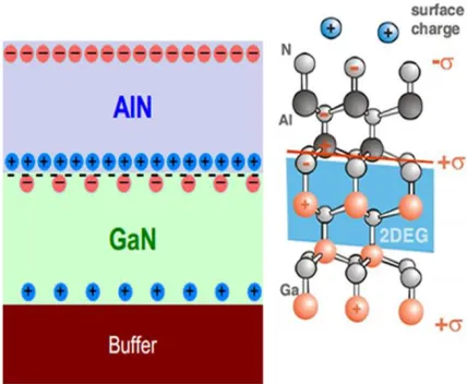
Charge polarization is a significant property of the III-V nitride semiconductors [21].
Due to the difference in the ionicity of the two atoms, the bonds in all III-V or II-VI
compound semiconductors are polar. There are two types of polarizations, spontaneous
and piezoelectric polarization. The piezoelectric polarization is produced due to the
lattice mismatch. The condition for spontaneous polarization is the c/a ratio must differ
from the ideal ratio of √8 3⁄ [22].
GaN and AlN are wurtzite crystal systems. The lattice constant a is the edge length of
basal plane, and c is unit cell height. All the nitrides have lower c/a ratio than ideal,
which is necessary for stability. The magnitude of the spontaneous polarization of GaN is
around 0.034 C/m2, but in AlN it is much bigger, ~0.09 C/m2, the largest value in all
nitrides because of the largest deviation from the ideal c/a ratio. Polarization induces
surface charges, shown in Fig. 1.6. An electric field is induced owing to the surface
charges, which leads to the tilt of band structure. Clearly, the band structures of AlInN
and AlN in Fig. 1.5 are both tilted.
The formation of 2DEG at the interface arises from the existence of donor states on the
AlInN surface [21]. An electron in a surface state can be excited to the conduction band
of AlInN with the help of induced electric field by surface charge, where it will flow to
the GaN side and accumulate at the interface to form the 2DEG. The carrier density can
polarized 2DEG can be realized without doping, which greatly reduces the scattering
from impurities.
Figure 1.6 Polarization and surface charge of GaN and AlN.
1.3 LANDAU LEVEL AND SHUBNIKOV-DE HAAS OSCILLATION
Classically, a free electron executes a circular motion in a perpendicular magnetic field
due to the Lorentz force 𝐹 = −𝑒𝑣 × 𝐵⃑ . The cyclotron frequency is 𝜔𝑐 = 𝑒𝐵 𝑚⁄ . In the
quantum mechanics, we need to solve the Schrödinger equation.
𝐻̂𝛹 = 𝐸𝛹 (1.12)
Here 𝛹 is the electronic wave function. The Hamiltonian is 𝐻̂ =2𝑚1 (𝑃̂ − 𝑞𝐴 )2. Where 𝑃⃑
is the momentum operator and 𝐴 is the vector potential which is related to the magnetic
For simplicity, the Landau gauge is used 𝐴 = (
0 𝐵𝑥
0
). Then the Hamiltonian becomes
𝐻̂ = 𝑝̂𝑥2
2𝑚+ 1
2𝑚(𝑝̂𝑦− 𝑞𝐵𝑥̂)2 (1.13)
Solving this Schrödinger equation will give the eigenenergy. In fact, this is same to the
Harmonic oscillation. So the energies are
𝐸𝑛 = (𝑛𝐿+ 1/2)ℏ𝜔𝑐. (1.14)
Here 𝑛𝐿=0, 1, 2, 3…; ℏ is the reduced Planck constant, 𝜔𝑐 = 𝑒𝐵 𝑚⁄ ∗ is the cyclotron
frequency. e is the electron charge and 𝑚∗ is the effective mass of carriers. In quantum
mechanics, the magnetic flux is quantized and the band structure becomes quantized
Landau level. The Landau energy 𝐸𝑛 is linearly proportional to magnetic field B and
index nL. The space between each Landau level is equal, as shown in Fig. 1.7(a).
Figure 1.7 (a) Landau levels. EF is the Fermi energy. (b) Shubinikov de Haas
For each Landau level, the degeneracy in unit area is 𝑁 =𝑔∅𝑠𝐵
0 =
𝑔𝑠𝐵𝑒
2𝜋ℏ . Here gs
represents a factor of 2 due to spin degeneracy for conventional 2DEG. For graphene,
𝑔𝑠 = 2 × 2 = 4 because of double spin and double valley degeneracy. The degeneracy is
proportional to magnetic field. When magnetic field is increased, the degeneracy is also
increased. That means there are more states in each Landau level and more carriers can
occupy the same Landau level.
For a system, the charge carrier density is constant at a certain temperature. Since each
state can only have 2 carriers due to spin degeneracy, the number of filled states below
Fermi energy EF is also constant. When the magnetic field B is increased, the degeneracy
for each Landau level will be also increased. Hence the Fermi level EF will drop to lower
value with increasing magnetic field B. When EF passes through a Landau level from
higher energy, the measured resistance oscillates periodically. This is called
Shubnikov-de Haas (SdH) oscillation.
It is important to know that at high magnetic fields, the carriers in the interior region
execute cyclotron motion. But at the boundaries, orbital motion is disrupted and the
carriers get scattered forward along the edge leading to a large conductance. When the
Fermi energy is between two Landau levels, the edge state related carriers dominate the
conduction, so the resistance is very small which corresponds to the minima in the
longitudinal resistance Rxx in Fig. 1.7(b). When the Fermi energy moves to inside of
Landau level, the scatterings due to interior carriers become strong and result in a high
In fact, SdH oscillation is a periodic function of 1/B, instead of magnetic field B. And
the frequency BF is directly proportional to carrier density 𝑛𝑆𝑑𝐻 = 𝑔𝑠𝑒𝐵𝐹⁄(2𝜋ℏ). So the
carrier density can be obtained by the SdH oscillation without measuring the Hall
voltage.
The amplitude of SdH oscillation can be expressed by
∆𝑅𝑥𝑥 = 4𝑅0sinh(𝜒)𝜒 exp (𝜔−𝜋
𝑐𝜏𝑞) (1.15)
Here 𝜒 = 2𝜋2𝑘𝐵𝑇 ∆𝐸⁄ and the Landau level energy spacing ∆𝐸 = ℏ𝜔𝑐 = ℏ𝑒𝐵 𝑚⁄ ∗.
𝑘𝐵is the Boltzmann constant, ℏ is the Planck constant, e is the electron charge and 𝜏𝑞is
the quantum lifetime. The temperature dependent SdH oscillation is useful to analyze the
Fermi surface, effective mass 𝑚∗and quantum scattering mechanism.
1.4 GRAPHENE
Graphene is made of a single layer of carbon atoms, with a hexagonal lattice structure as
shown in Fig. 1.8(a). Atom A (red) and atom B (blue) are inequivalent, so the graphene
structure can be viewed as a triangular lattice with a basis of two atoms A and B.
The Bravais lattice vectors are [11]
𝑎 1 =𝑎2(3, √3), 𝑎 2 =𝑎2(3, −√3) (1.16)
Where a ~1.42 Å is the nearest carbon to carbon distance.
The reciprocal lattice vectors are
so the first Brillouin zone can be drawn and it is hexagonal as shown in Fig. 1.8(b).
Figure 1.8 (a) Honeycomb lattice of graphene, with two types of atoms A and B. 𝑎 1 and 𝑎 2 are lattice vectors. (b) The reciprocal lattice vectors and the 1st Brillouin zone
[11].
For each carbon atom, there are four valence electrons. Three electrons form the
chemical bonds in the plane, named σ bonds. These three σ bonds are localized and
cannot contribute to the electronic conduction. The 2pz orbital is oriented perpendicular to
the plane, which is free to move, and forms the π band.
The energy bands derived using the nearest neighbor tight-binding method are [11,23]
𝐸(𝑘⃑ ) = ±𝑡√3 + 2 cos(√3𝑘𝑦𝑎) + 4cos (√32𝑘𝑦𝑎)cos (32𝑘𝑥𝑎) (1.18)
Here t is the nearest neighbor hopping energy. The energy band is plotted in Fig. 1.9.
𝐸 < 0 is the valence band, 𝐸 > 0 is conduction band. The two bands touch each other at
the six corners (Dirac points). The gap in graphene vanishes and graphene is not a
negative energy band is fully filled while the positive band is empty (electron - hole
symmetry). The Fermi energy is 𝐸𝐹 = 0 at zero temperature.
The positions of Dirac points K and 𝐾′ shown in Fig. 1.8(b) in momentum space are
given by [11]
𝑲 =2𝜋3𝑎(1,√31) , 𝑲′= 2𝜋 3𝑎(1, −
1
√3) (1.19)
For the region near K and 𝐾′, the energy dispersion, if we only take the first order, can be
expanded as [11,23]
𝐸(𝑘⃑ ) ≈ ±ℏ𝑣𝐹|𝑘⃑ | (1.20)
The energy surface is plotted in Fig. 1.9 and consists of two circular cones touching each
other at 𝐸 = 0. Furthermore, this is very similar to the linear dispersion relation of
photons where the speed of light c is replaced by the Fermi velocity 𝑣𝐹. For graphene,
𝑣𝐹 = 3𝑡𝑎 2~10⁄ 6𝑚/𝑠 [11], very large speed compared to the conventional 2DEG, so the
carriers at the Dirac points in graphene behavior like massless particles.
When the graphene is placed in the magnetic field B, the energy is also quantized to
Landau levels. Unlike the conventional 2DEG, the Landau levels of graphene in a
magnetic field are [11,25]
𝐸𝑛 = ±𝑣𝐹√2𝑒ℏ𝐵𝑛𝐿 (1.21)
Here the Landau index 𝑛𝐿= 0, 1, 2,…, e is the charge of electron, ℏ is the reduced Planck
constant. ± is the band index and refers to the conduction (electrons) / valence (holes)
band. The Landau level is proportional to the square root of magnetic field B and index
𝑛𝐿, unlike the linear relation of massive quasi-particles 𝐸𝑛 = (𝑛𝐿+12) ℏ𝜔𝑐. The gaps
between Landau levels in graphene are not equal, as shown in Fig. 1.10. Remarkably,
there exists a zero-energy Landau level in graphene when 𝑛𝐿=0 and it is independent on
the magnetic field [25].
1.5 WEAK LOCALIZATION
At low temperatures phonon scattering is suppressed, which induces a long mean free
path and coherence length. So the wavelike nature of charge carriers at low temperature
becomes important. In this regime, due to constructive quantum interference, the carrier
has an enhanced probability to be scattered back to the origin along a closed loop in
opposite directions, resulting in a larger resistivity compared to the Drude model. This is
called weak localization and widely observed in disordered systems [26,27].
The probability for a carrier propagating from point A to B, as shown in Fig. 1.11(a), is
the sum of all the Feynman’s paths between A and B [18]
𝑃 = |∑ 𝐴𝑖 𝑖|2 = ∑ |𝐴𝑖 𝑖|2+ ∑𝑖≠𝑗𝐴𝑖𝐴𝑗∗ (1.22)
Here 𝐴𝑗 = |𝐴𝑗|𝑒𝑖𝜑𝑗 = |𝐴𝑗|𝑒𝑖𝑘⃑ 𝑗𝑙 𝑗 is the propagation amplitude along path j. The first term
is the classical probability, and second term is interference part. For each path the carrier
experiences diffusive motion like a random walk. Because the scattering is elastic, the
phase acquired along any path is well defined, but different along each Feynman path.
When averaged over a large number of paths, the interference term vanishes.
However, there is a special case. For self-crossing trajectories, just like point O as
shown in Fig. 1.11(b), the electron can be scattered along clockwise or counterclockwise
back to the origin O. The phases ∆𝜑 acquired in these two directions are exactly same,
because the propagation 𝑝 → −𝑝 , 𝑑𝑙 → −𝑑𝑙 . It can be viewed as a motion of a carrier
and its time-reversed counterpart. Hence this constructive interference has time reversal
|𝐴+𝑝+ 𝐴−𝑝|2 = |𝐴+𝑝|2+ |𝐴−𝑝|2+ 2𝐴+𝑝𝐴−𝑝∗
= |𝐴+𝑝|2+ |𝐴−𝑝|2+ 2|𝐴+𝑝|𝑒𝑖(𝜑+∆𝜑) |𝐴
−𝑝|𝑒−𝑖(𝜑+∆𝜑)= 4|𝐴𝑝| 2
(1.23)
Here|𝐴+𝑝|=|𝐴−𝑝|. The probability of a carrier to be scattered back to the origin is 4 times
as large as the classical value. This coherent back-scattering leads to an increase in
resistance compared with the classical Drude model. The condition for weak localization
to occur is that the phase coherence length should be much longer than the mean free path
so that the carrier can return to the origin after several times of scattering [27].
Weak localization can be suppressed at high temperature. Inelastic scattering such as a
collision with a phonon or another electron can change the momentum of the carrier
which destroys the phase coherence. When the temperature is increased, scattering
becomes strong and the coherence length is reduced. So the effect of weak localization
becomes weak.
The application of a magnetic field can also affect the weak localization, because the
magnetic field breaks the time reversal symmetry and destroys the interference. Hence
with increasing magnetic field, the probability of back scattering is decreased, which
leads to an increase in the magnetoconductivity. The change of magnetoconductivity
[5,28,29] is
∆𝜎𝑥𝑥 = 𝜎𝑥𝑥(𝐵) − 𝜎𝑥𝑥(0) = 𝑒
2
𝜋ℎ[𝜓 ( 1 2+
ℏ
4𝑒𝐷𝐵𝜏𝑖) − 𝜓 (
1 2+
ℏ
4𝑒𝐷𝐵𝜏𝑒) + ln (
𝜏𝑖
Here 𝜓is the digamma function; 𝜏𝑖 and 𝜏𝑒 are the inelastic and elastic scattering times
respectively; D is the diffusion constant. The elastic scattering time and the inelastic
phase breaking time can be readily obtained from the magnetoconductivity measurement.
Figure 1.11 (a) Feynman’s paths of a carrier propagating from A to B. The straight line between two scatterings represents the diffusive motion of carrier, just like a series of random walks. (b) A pair of closed paths at point O that contribute to weak localization.
For graphene, the weak localization is strongly modified due to valley degeneracy.
Graphene lattice can be considered as a superposition of two identical sub-lattices with
two atoms since atoms A and B are inequivalent. The two sublattices are like two degrees
of freedom. The electron can have amplitude to be on the sublattice A, and an amplitude
on sublattice B. The two components of the electronic wave function on them can be
analogous to the two spins ± 12, called pseudo spin [30]. If all the electronic density is
located on the A sublattice, this can be viewed as an “up” pseudo spin state, whereas
density solely on the B sublattice corresponds to a “down” pseudo spin. In graphene,
electronic density is usually shared equally between A and B sublattices, so that the
pseudo spin part of the wave function is a linear combination of “up” and “down”, and it
lies in the plane of the graphene sheet [31,32], as shown in Fig. 1.12. Furthermore,
related to the direction of electronic momentum, either parallel or antiparallel to each
other [31].
Figure 1.12 Pseudo spin of graphene [31].
When a carrier in graphene is scattered back to the origin after a series of scatterings,
the momentum changes from 𝑝 → −𝑝 . Due to the chiral symmetry, the pseudo spin
must also change to the opposite direction so that the pseudo spin remains parallel to the
momentum. Hence for a clockwise path the pseudo spin rotates by an angle of –π, for a
counterclockwise path the pseudo spin rotates by π. So the difference in the angle of
pseudo spin rotation for the two paths is 2π. The net rotation of the pseudo spin by 2π
induces a phase difference of π between the two paths [32,33]. This is analogous to the
rotation by 2π of a spin–1/2 particle because a rotation by 2π doesn’t return wave
function to its origin state [34]. Hence the returning electron is out of phase, resulting in
Figure 1.13 Chirality of graphene at Dirac points K and 𝐾′. Intravalley and intervalley scatterings play an important role in weak localization effect.
However, the trigonal warping effect [11,35] can break the time-reversal symmetry
(the absence of 𝑝 → −𝑝 symmetry) of the electronic dispersion within a single valley.
Furthermore, elastic intravalley scattering can break the chiral symmetry. These two
effects can suppress the weak antilocalization effect [36].
A carrier can be scattered from K to 𝐾′, flipping the chirality. This is called intervalley
scattering. In this process, the momentum has changed direction due to back scattering,
but the psudospin has the same direction. So the phase acquired by two closed loops
remains the same, resulting in the constructive interference and restoration of the
conventional weak localization.
Hence due to the chiral nature of carriers in monolayer graphene, weak antilocalization
is expected. However, trigonal warping and intravalley scattering suppresses
antilocalization and intervalley scattering restores conventional weak localization. The
∆𝜎(𝐵) =𝜋ℎ𝑒2[𝐹 (𝐵𝐵
𝜙) − 𝐹 (
𝐵
𝐵𝜙+2𝐵𝑖) − 2𝐹 (
𝐵
𝐵𝜙+𝐵∗) (1.25)
𝐹(𝑧) = 𝑙𝑛𝑧 + 𝜓(12+1𝑧), 𝐵𝜙,𝑖,∗ = ℏ
4𝐷𝑒𝜏𝜙,𝑖,∗ −1
Here 𝜓(𝑧) is the digamma function,𝜏𝜙is the inelastic phase breaking time, 𝜏𝑖 is the
(elastic) intervalley scattering time, 𝜏∗−1 = 𝜏𝑖−1+ 𝜏𝑤−1+ 𝜏𝑧−1, where 𝜏𝑤 is related to
trigonal warping which breaks 𝑝 → −𝑝 symmetry of the electronic dispersion and 𝜏𝑧 is
the intravalley scattering time. D is the diffusion constant given by 𝐷 = 𝑣𝐹2𝜏 2⁄ . 𝜏 is the
transport scattering time obtained from the carrier mobility. Compared to the
CHAPTER 2
DEVICE FABRICATION AND TRANSPORT MEASUREMENT
In this chapter, the fabrication of samples, including monolayer graphene with antidots
and a Hall bar of AlInN/GaN heterostructure, is described in detail. The low temperature
and high magnetic field techniques are also explained.
2.1 FABRICATION AND CHARACTERIZATION OF GRAPHENE WITH
ANTIDOTS
Graphene sample is commercial monolayer graphene on Si/SiO2 substrate (Graphene
Supermarket Inc.), grown by the Chemical Vapor Deposition (CVD) method. The antidot
lattice on graphene was fabricated by the electron beam lithography followed by reactive
ion etching with oxygen plasma at the USC Nanocenter. A more detailed description can
be found in Appendix A.
Figure 2.1 shows the Scanning Electron Microscope (SEM) images of the antidot
lattice. The images are obtained by Zeiss Ultraplus Thermal Field Emission Scanning
Electron Microscope. The grey region is graphene. However the white region is empty,
where the graphene has been etched away by oxygen plasma. We can clearly see 4 Hall
bars at up and down sides. The high magnification image of antidots, with the radius
Figure 2.1 (a) Graphene antidots with Hall bars. (b) High magnification SEM image of antidots.
Raman spectroscopy (JY Horiba with a HeNe laser) of monolayer graphene is shown
in Fig. 2.2. Clearly there are two prominent peaks. The band at ~2663 cm-1 is called the
2D peak which is due to the second order of zone-boundary phonons; the one at ~1602
cm-1 is G peak or Graphite peak [40]. The intensity ratio between 2D and G peak is an
important indicator of the numbers of graphene layer. Monolayer graphene usually has a
stronger 2D peak than a G peak. The intensity of the 2D peak decreases for a bilayer,
triple layer and so on. The intensity high ratio between the 2D band and G band shows
2.2 FABRICATION OF ALINN/GAN DEVICE
The Al0.83In0.17N/GaN epilayer structures were grown on a sapphire substrate by
standard metal-organic chemical vapor deposition (MOCVD) process. Our AlInN/GaN
wafers were obtained from Dr. Asif Khan at the Electrical Engineering Department of
USC. A SEM image of the cross section view of such heterostructure is provided in Fig.
2.3(a). It clearly shows a ~200 nm AlN buffer layer followed by ~2.2 μm undoped GaN
as channel layer, ~1 nm AlN spacer and ~7 nm AlInN barrier layer with In composition
of 17%.
In order to measure the transport properties, I fabricated a Hall bar using
photolithography. The Hall bar mesa was etched by an inductive coupled plasma etching
machine using Cl2/BCl3. A more detailed description is given in Appendix B. Fig.2.3(b)
is a schematic diagram of our Hall bar.
Figure 2.3 (a) SEM image of cross section of AlInN/GaN heterostructure. (b) Schematic diagram of a Hall bar.
Artificial opals are self-organized, close packed materials which are built up by
nanoscale regular spheres. Figure 2.4 shows the structures of opal obtained by scanning
electron microscope (Zeiss Ultra Plus FESEM). The opals are arranged in the hexagonal
close-packed lattice. The diameter of the spheres is around 200 nm.
Figure 2.4 SEM images of artificial opal.
Our 3-dimensional carbon nanostructures were produced by infiltrating carbon into the
porous matrix of artificial opals by chemical vapor deposition (CVD) of propylene gas
and then removing the silica spheres with hydrofluoric acid [41]. The diameter of the
spheres can be varied. The diameter of carbon inverse structure shown on the right of Fig.
2.5 is around 245 nm. We can also observe a mix of two structures, cubic and hexagonal.
2.4TRANSPORTMEASUREMENTTECHNIQUES
In our transport measurement, a 4- probe method is employed. The reason for using a
4-probe method instead of probe is to reduce the contact resistance effect. In the
2-probe method shown in Fig. 2.6(a), a voltage source is applied to the sample and the
current I is measured using Ampere meter. The current is determined not only by the
sample resistance Rs, but also by the contact resistances Rc1 and Rc2, which are all
unknown. The measured current is smaller due to contact resistances. If we still use
𝑅 =𝑉𝐼 the resistance obtained is larger than the real sample resistance. However in the
4-probe method, a current source is applied, so the contact resistances Rc1 and Rc2 cannot
affect the measured current I. When measuring the voltage on the sample, the contact
resistances, Rc3 and Rc4, are much smaller than the impedance of the volt meter. Thus the
resistance obtained by 𝑅 =𝑉𝐼 is the real sample resistance.
Figure 2.6 (a) 2-probe method, (b) 4-probe method.
Figure 2.7(a) shows the schematic diagram of probe connections for AlInN/GaN
current source. The pair of probes on the same side are used to measure the longitudinal
voltage Vxx and the two pads on opposite sides are for measuring the Hall voltage VH.
The magnetic field B is perpendicular to the sample surface, but we can also rotate the
sample so that the orientation dependence of transport properties is obtained. Figure 2.7(b)
shows a graphene sample with six gold pads connected to an 8-pin dip socket by
aluminium wires. The size of the silicon substate is around 5 mm × 5 mm × 1 mm.
Figure 2.7 (a) schematic diagram of probe for the AlInN/GaN heterostructure. (b) Graphene sample on an 8-pin dip socket.
To reduce the noise and obtain a clean signal, we use lock-in amplifiers to measure the
voltages. A 120 µA input current at 17.37 Hz was applied by the lock-in amplifier
(Stanford SR850 DSP). The electrical and magneto transport measurements were
conducted using an 18/20 Tesla General Purpose Superconducting Magnet (SCM2) and a
31 Tesla, 50 mm Bore Magnet (Cell 9) at the National High Magnetic Field Laboratory at
CHAPTER
3
QUANTUM
TRANSPORT
IN
A
LI
NN/G
AN
HETEROSTRUCTURES
The AlInN/GaN heterostructure is a wide band gap semiconductor that has great
potential in high power and high frequency applications. In this chapter, I discuss my
measurements of the transport properties of the two-dimensional electron gas in
AlInN/GaN heterostructures at low temperatures. From the Shubnikov-de Haas
oscillation and the change of the magnetoconductivity due to weak localization, I
calculated the effective mass of the electrons and scattering times. The dominant
scattering mechanisms at low temperatures have been determined.
3.1 TEMPERATURE DEPENDENT ELECTRICAL TRANSPORT
The typical temperature dependence of sheet resistance, R□ is shown in Fig. 3.1(a).
Here sheet resistance is calculated by 𝑅□ =𝑅𝑥𝑥𝐿𝑊, where Rxx is the longitudinal resistance
measured at zero-magnetic field; W=165 𝜇𝑚 is the width of Hall bar; and L=770 𝜇𝑚 is
the length labeled in the figure. Generally the sheet resistance increases with increasing
temperature above 20 K, consistent with metallic-like transport. The variation of the Hall
carrier density as a function of temperature is shown in Fig. 3.1(b). The carrier density n
is obtained by 𝑅𝐻= 𝑛𝑒𝐵, where RH is the Hall resistance, e is the charge of the electron
the change is very small. This is because the band gap is Eg~ 4 eV [6,42], much larger
than 𝑘𝐵𝑇.
Figure 3.1 (a) Temperature dependent sheet resistance, inset is the schematic diagram of structure. (b) Carrier density and Hall mobility as a function of temperature.
In contrast, the Hall mobility decreases with increasing temperature, and the
mobility is weakly temperature dependent. It decreases slightly with increasing
temperature, mirroring that of the sheet resistance. As will be discussed later, these
behaviors may arise from impurity scattering or surface roughness as well as
electron-electron scattering. Between 20 K and 100 K, the temperature dependence is more
pronounced. As shown in the inset of Fig. 3.1(b), the inverse mobility is directly
proportional to temperature, 𝜇−1 ∝ 𝑇, indicating that acoustic phonon scattering is
dominant [43-45]. Such temperature dependence has been widely observed in
AlGaN/GaN heterostructures. At higher temperatures, above 100 K, the mobility
decreases even faster and an exponential dependence 𝜇−1∝ 𝑒𝑎𝑇 describes the data very
well. In the 2DEG literature, such exponentially temperature dependent mobility at high
temperatures has been attributed to polar optical phonon scattering [44,46].
3.2 SHUBNIKOV-DEHAASOSCILLATION
The longitudinal resistance Rxx as a function of applied magnetic field B up to 18 T at
different temperatures is shown in Fig. 3.2(a). As the magnetic field is increased,
Shubnikov-de Haas (SdH) oscillations appear. The peaks of the oscillations are
pronounced at low temperatures and damped with increasing temperature. This effect of
temperature is more apparent if we subtract the background from Rxx, (Fig. 3.2(b)). SdH
oscillations are a periodic function of 1/B. Evidence of multiple subbands in AlInN/GaN
or AlGaN/GaN heterostructures has been reported [28,47]. However, Fourier Transform
inset of Fig. 3.2(b). This indicates that only one band is dominant in our sample. Also the
frequency BF is directly related to the carrier density by
𝑛𝑆𝑑𝐻 = 2𝑒𝐵𝐹⁄ℎ (3.1)
The factor of two is due to spin degeneracy. Hence the carrier density of this sample is
𝑛𝑆𝑑𝐻 = 1.948 × 10¹³𝑐𝑚−2. This agrees very well with the average value obtained from
our Hall measurement.
Figure 3.2 (a) Magnetoresistance up to 18 T at a set of temperatures. (b) Shubnikov-de Haas oscillations after subtracting the background.
The amplitude of the SdH oscillation is given by [48,49]
∆𝑅𝑥𝑥 = 4𝑅0sinh(𝜒)𝜒 exp (𝜔−𝜋
𝑐𝜏𝑞) (3.2)
Here 𝜏𝑞is the quantum lifetime, which will be discussed later. 𝜒 = 2𝜋2𝑘𝐵𝑇 ∆𝐸⁄ and the
The effective mass 𝑚∗of electrons can be extracted from the temperature dependence
of the SdH amplitude at a constant magnetic field by examing the following ratio [9]
∆𝑅𝑥𝑥(𝑇,𝐵)
∆𝑅𝑥𝑥(𝑇0,𝐵)=
𝑇𝑠𝑖𝑛ℎ(𝜒(𝑇0))
𝑇0 sinh (𝜒(𝑇)) =
𝑇 sinh (2𝜋2𝑘
𝐵𝑇0⁄∆𝐸(𝐵))
𝑇0 sinh (2𝜋2𝑘𝐵𝑇 ∆𝐸(𝐵))⁄ (3.3)
Here we chose the lowest temperature, 0.27 K, as T0. Figure 3(a) shows the above ratio of
amplitude at T0= 0.27 K and B= 17.7 T. Analyzing our data using Eq. (3.3) we can
extract ∆𝐸(𝐵). The inset of Fig. 3.3(a) shows the field dependence of Landau level
energy gap. Thus the corresponding effective mass is 𝑚∗ = (0.2327 ± 0.0019)𝑚𝑒,
similar to the values reported in AlInN/GaN heterostructures which are 0.22𝑚𝑒and
0.25𝑚𝑒 [47,50] and in AlGaN/GaN systems which are 0.23𝑚𝑒 and 0.24𝑚𝑒 respectively
[5,51].
The quantum lifetime is obtained from the slope of the Dingle plot, as shown in Fig.
3.3(b), because
𝑙𝑛𝔇 = ln [∆𝑅(𝑇,𝐵)sinh (2𝜋2𝑘𝐵𝑇 ∆𝐸(𝐵))⁄
2𝜋2𝑘𝐵𝑇 ∆𝐸(𝐵)⁄ ] = 𝐶0−
𝜋𝑚∗
𝑒𝜏𝑞𝐵 (3.4)
where 𝔇 is the expression within the bracket, C0 is a constant. In this sample the quantum
lifetime is 𝜏𝑞 = 0.0350 ± 0.0017 𝑝𝑠 . Furthermore, 𝜏𝑞 also determines the Dingle
temperature 𝑇𝐷 = ℎ (4𝜋⁄ 2𝑘𝐵𝜏𝑞), which is a measure of the disorder. At T = 0.27 K, we
find a relatively high value 𝑇𝐷 = 34.7 K. Also the broadening of the Landau levels
[48,49], as determined by kBTD ~3 meV, is not much smaller than the Landau level
spacing ∆𝐸(𝐵) = 9.04 𝑚𝑒𝑉 at 17.7 T. This may explain the relatively small amplitude
Figure 3.3 (a) Effective mass plot at 17.7 T, where the data are best fit to Eq. (3.3); Inset is field dependence of the Landau level spacing. (b) Dingle plot to obtain the quantum
lifetime in AlInN/GaN heterostructure.
It is instructive to compare the quantum relaxation rate to transport rate, since
1 𝜏⁄ 𝑞= ∫ 𝑃(𝜃)𝑑θ
1 𝜏⁄ = ∫ 𝑃(𝜃)(1 − 𝑐𝑜𝑠𝜃)𝑑θ𝑡 (3.5)
where 𝑃(𝜃) is the probability of scattering through an angle 𝜃. The quantum lifetime 𝜏𝑞
includes information of all scatterings; however the transport lifetime 𝜏𝑡 (from Hall
mobility) is weighted by the scattering angle and mainly determined by large angle
scattering [51-53]. The transport lifetime 𝜏𝑡= 0.252 𝑝𝑠 is nearly an order of magnitude
larger than the quantum lifetime. In particular the ratio 𝜏𝑡⁄𝜏𝑞 = 7.2 indicates that small
angle scattering associated with long range interactions due to distant ionized impurities
3.3 WEAK LOCALIZATION
As is evident from Fig. 3.2(a), at low magnetic fields Rxx decreases with the applied
field; that is conductivity goes up with increasing field. This negative magnetoresistance
arises from weak localization. It is convenient to define the magnetoconductivity by
𝜎𝑥𝑥 = 𝜌𝑥𝑥⁄(𝜌𝑥𝑥2 + 𝜌𝑥𝑦2 ). The quantum correction to the change in magnetoconductivity at
low magnetic fields is [5,28,29,54]
∆𝜎𝑥𝑥 = 𝜎𝑥𝑥(𝐵) − 𝜎𝑥𝑥(0) = 𝑒
2
𝜋ℎ[𝜓 ( 1 2+
ℏ
4𝑒𝐷𝐵𝜏𝑖) − 𝜓 (
1 2+
ℏ
4𝑒𝐷𝐵𝜏𝑒) + ln (
𝜏𝑖
𝜏𝑒)] (3.6)
Here 𝜓 is the digamma function; 𝜏𝑖 and 𝜏𝑒 are the inelastic and elastic scattering times
respectively; D is the diffusion constant given by 𝐷 = 𝑣𝐹2𝜏 𝑑⁄ = 𝑣𝐹2𝜏 2⁄ , where d is the
dimensionality and for our two-dimensional (d = 2) system the Fermi velocity is
𝑣𝐹 = ℏ𝑘𝐹⁄𝑚∗ = ℏ√2𝜋𝑛 𝑚⁄ ∗ (3.7)
Here 𝑣𝐹 = 0.5504 × 10⁶𝑚/𝑠. By choosing parameter values estimated earlier 𝜏 ≡ 𝜏𝑡 =
0.252 𝑝𝑠, we determined 𝐷 = 0.03817𝑚2/𝑠 and the mean free path 𝑙 = 𝑣𝐹𝜏𝑡= 139 𝑛𝑚
[10].
The inelastic and elastic scattering times were computed from the best fit analysis of
experimental data to Eq. (3.6). ∆𝜎𝑥𝑥 for a set of temperatures is shown in Fig. 3.4(a). For
a constant temperature the conductivity increases with increasing magnetic field, and at
higher temperature, the conductivity is reduced. We find that Eq. (3.6) describes the
experimental data very well for temperatures below 20 K, which allows us to obtain the
values of the relaxation times. Interestingly the elastic scattering time 𝜏𝑒 is constant with
roughness scatterings. Also 𝜏𝑒 = 0.144𝑝𝑠 is the same order as the transport time 𝜏𝑡.
However, the inelastic scattering time 𝜏𝑖𝑛 is much larger than the elastic scattering time
and the transport time at low temperatures. This is necessary because the phase coherence
length should be long enough so that the carrier can be scattered back to the origin after
several scatterings. In addition 𝜏𝑖𝑛 decreases with increasing temperature. In fact, the
inelastic scattering rate is linearly proportional to temperature,𝜏𝑖𝑛−1∝ 𝑇, as shown in
Fig. 3.4(b). This linearity has been attributed to phase breaking by inelastic
electron-electron scattering [28,55,56].
Figure 3.4 (a) Magnetoconductivity at low magnetic fields for several temperatures. (b) The inelastic scattering rate displays linear temperature dependence. Insets are the
zero-field resistance and conductivity respectively.
The effect of electron-electron scattering is also observed in the absence of the
magnetic field. As shown in the inset of Fig. 3.4(b), the sheet resistance at low
temperatures is non-monotonic. With increasing temperature it first decreases until 20 K
𝜎𝑥𝑥(𝐵 = 0) = lim𝐵→0𝜋ℎ𝑒2[𝜓 (12+4𝑒𝐷𝐵𝜏ℏ
𝑖𝑛) − 𝜓 (
1 2+
ℏ
4𝑒𝐷𝐵𝜏𝑒)] ≅ −
𝑒2
𝜋ℎ𝑙𝑛 𝜏𝑖𝑛
𝜏𝑒 (3.8)
since 𝜓(𝑥) → 𝑙𝑛𝑥 𝑤ℎ𝑒𝑛 𝑥 ≫ 1.
As stated above, 𝜏𝑖𝑛 ∝ 𝑇−1, thus 𝜎𝑥𝑥(0) ∝ 𝑙𝑛𝑇 [58]. The conductivity at zero-field is
plotted as a function of lnT in the inset of Fig. 3.4(b). Clearly below 20 K, 𝜎𝑥𝑥(𝐵 = 0)
displays a linear dependence, characteristic of weak localization. Hence at low
temperatures, we observed the experimental evidence of weak localization in zero-field
transport as well as the magnetotransport in our AlInN/GaN system, both hallmarks of
electron-electron scattering.
3.4 ANGLE DEPENDENCE
To further investigate weak localization behavior, we varied the angle θ between
magnetic field and the normal to the surface of sample. Figure 3.5 shows the
angle-dependent resistance at T = 2 K. At 0, when magnetic field is perpendicular to the
sample, the magnetoresistance is pronounced and similar to the behavior described
earlier. With the increase of tilt angle, the influence of the magnetic field becomes
smaller and weak localization is maintained over higher magnetic fields. At the highest
tilt angle (θ = 88), effects of weak localization dominate the entire field regime such that
the resistance continues to decrease with increasing magnetic field, displaying a negative
magnetoresistance even up to 18 T. The crossover field where the magnetoresistance is
lowest displays the anticipated linear dependence on 1/cosθ. Furthermore, the SdH
oscillations disappear gradually with increasing angle. If we plot the magnetoresistance


![Figure 1.4 Band diagram of the interface between n-doped AlGaAs and intrinsic GaAs [18]](https://thumb-us.123doks.com/thumbv2/123dok_us/8393695.1385575/28.612.188.434.438.633/figure-band-diagram-interface-doped-algaas-intrinsic-gaas.webp)


![Figure 1.9 Energy band derived from the nearest-neighbor tight binding model [24]. Zoomed in figure is the band structure around Dirac points K](https://thumb-us.123doks.com/thumbv2/123dok_us/8393695.1385575/35.612.199.417.517.661/figure-energy-derived-nearest-neighbor-binding-zoomed-structure.webp)
![Figure 1.10 Landau level in the magnetic field. Each level is not equally spaced; instead it is proportional to square root of B [25]](https://thumb-us.123doks.com/thumbv2/123dok_us/8393695.1385575/36.612.132.491.431.623/figure-landau-magnetic-equally-spaced-instead-proportional-square.webp)


