Notice
While reasonable efforts have been made to assure the accuracy of this document, Motorola, Inc. assumes no liability resulting from any omissions in this document, or from the use of the information obtained therein. Motorola reserves the right to revise this document and to make changes from time to time in the content hereof without obligation of Motorola to notify any person of such revision or changes. No part of this material may be reproduced or copied in any tangible medium, or stored in a retrieval system, or transmitted in any form, or by any means, radio, electronic, mechanical, photocopying, recording or facsimile, or otherwise, without the prior written permission of Motorola, Inc.
It is possible that this publication may contain reference to, or information about Motorola products (machines and programs), programming, or services that are not announced in your country. Such references or information must not be construed to mean that Motorola intends to announce such Motorola products, programming, or services in your country.
Restricted Rights Legend
If the documentation contained herein is supplied, directly or indirectly, to the U.S. Government, the following notice shall apply unless otherwise agreed to in writing by Motorola, Inc.
Use, duplication, or disclosure by the Government is subject to restrictions as set forth in subparagraph (c)(1)(ii) of the Rights in Technical Data and Computer Software clause at DFARS 252.227-7013.
Preface
This document provides brief board level information and complete memory map descriptions for the Ultra 603, Ultra 603e, and Ultra 604 PowerPCTM series of
motherboard platforms.
This document is intended for anyone who wants to program the system board platform in order to design OEM systems, supply additional capability to an existing PC-compatible system, or work in a lab environment for experimental purposes.
A basic knowledge of computers and digital logic is assumed.
To use this document, you may wish to become familiar with the publications listed in the Related Documentation section in Appendix A.
Document Conventions
The following conventions are used in this document:
bold
is used for user input that you type just as it appears. Bold is also used for commands, options and arguments to commands, and names of programs, directories, and Þles.
italic
is used for names of variables to which you assign values. Italic is also used for comments in screen displays and examples.
courier
is used for system output (e.g., screen displays, reports), examples, and system prompts.
<RETURN> or <CR>
represents the carriage return key.
CTRL
Document Terminology
Throughout this document, a convention has been maintained whereby data and address parameters are preceded by a character which speciÞes the numeric format, as follows:
For example, Ò12Ó is the decimal number twelve, and Ò$12Ó is the decimal number eighteen. Unless otherwise speciÞed, all address references are in hexadecimal throughout this document.
An asterisk (*) following the signal name for signals which are level signiÞcant denotes that the signal is true or valid when the signal is low.
An asterisk (*) following the signal name for signals which are edge signiÞcant denotes that the actions initiated by that signal occur on high to low transition. In this document, assertion and negation are used to specify forcing a signal to a particular state. In particular, assertion and assert refer to a signal that is active or true; negation and negate indicate a signal that is inactive or false. These terms are used independently of the voltage level (high or low) that they represent.
Data and address sizes are deÞned as follows:
A byte is eight bits, numbered 0 through 7, with bit 0 being the least significant.
A two-byte is 16 bits, numbered 0 through 15, with bit 0 being the least significant. For other RISC modules, this is called a half-word.
A four-byte is 32 bits, numbered 0 through 31, with bit 0 being the least significant. For the other RISC modules, this is called a word.
An eight-byte is 64 bits, numbered 0 through 63, with bit 0 being the least significant. For the other RISC modules, this is called a double-word.
The computer programs stored in the Read Only Memory of this device contain material copyrighted by Motorola Inc., Þrst published 1991, and may be used only under license such as the License for Computer Programs (Article 14) contained in MotorolaÕs Terms and Conditions of Sale, Rev. 1/79.
!
WARNING
This equipment generates, uses, and can radiate magnetic energy. It may cause or be susceptible to electro-magnetic interference (EMI) if not installed and used in a cabinet with adequate EMI protection.
Motorola¨ and the Motorola symbol are registered trademarks of Motorola, Inc. AIXª, HALª, IBMª, OS/2ª, PC-ATª, PowerPC Architectureª, PowerPC 601ª, PowerPC 603ª, PowerPC 603eª, PowerPC 604ª, PS/2ª, and
RISCWatchª are trademarks or registered trademarks of International Business Machines Corporation.
PowerPCª is a trademark of International Business Machines Corporation, and is used by Motorola with permission.
Microsoftª, Windowsª, and Windows NTª are trademarks or registered trademarks of Microsoft Corporation.
Super I/Oª is a trademark of National Semiconductor Corporation.
TIMEKEEPERª is a registered trademark of SGS-Thomson Microelectronics. All other products mentioned in this document are for identiÞcation purposes only and are trademarks or registered trademarks of their respective holders.
© Copyright Motorola 1994, 1995
All Rights Reserved
Printed in the United States of America
List of Tables
Ultra 60x Features 1-2
Processor View of the Memory Map 1-6 PCI ConÞguration Space Map 1-8 ISA I/O Space Map 1-9
1
1
Product Description and
Memory Maps
Introduction
This chapter briefly describes the Ultra 603, Ultra 603e, and Ultra 604 PowerPC™ based motherboard platforms. Unless otherwise specified, both motherboard platforms are hereafter referred to as the system board platform. The chapter begins with a board level overview and features list and ends with a complete description of the memory maps, which are the major part of this chapter.
Overview
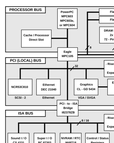
The system board platform is an all-in-one motherboard
implemented on a nine inch by thirteen inch single-plane printed circuit board. The system board platform accommodates either an MPC603, MPC603e, or MPC604 RISC processor for the MPU (factory-installed option) and an MPC105 PowerPC-to-PCI bridge as the memory controller between the processor (MPU) bus and the Peripheral Component Interconnect (PCI) (local) bus. An Intel i82378ZB PCI-to-ISA bridge component (referred to as the PIB) allows Industry Standard Architecture (ISA) bus-compatible peripherals to be accessed by the MPC60x processor. The system board platform also provides for the addition of a riser card which supports PCI bus and/or ISA bus cards.
Some of the standard PC (personal computer) interconnections that are included on the system board platform are:
❏ Two asynchronous serial ports
❏ One parallel port
❏ One IDE controller and connector
❏ Floppy disk controller and connector
❏ Keyboard
Product Description and Memory Maps
1
In addition to the standard PC interconnections, the system board platform also provides a SCSI-2 PCI controller with standard and wide connectors, an Ethernet PCI controller with 10Base-T and AUI connectivity, a graphics PCI controller with SVGA connector, as well as business audio input/output capabilities, all on the primary motherboard.
The system board platform is designed to support MicrosoftÕs Windows NTª and IBMÕs AIXª operating systems.
Another feature of the system board platform is that it can be available as either:
❏ a motherboard only,
❏ a motherboard integrated in a chassis, or
❏ a full computer system with motherboard, chassis, and
peripherals.
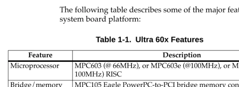
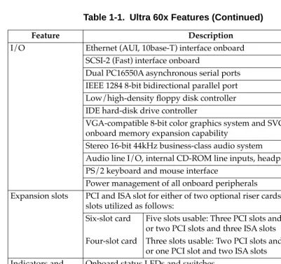
Features
The following table describes some of the major features of the system board platform:
Table 1-1. Ultra 60x Features
Feature Description
Microprocessor MPC603 (@ 66MHz), or MPC603e (@100MHz), or MPC604 (@ 100MHz) RISC
Bridge/memory controller
MPC105 Eagle PowerPC-to-PCI bridge memory controller
Memory bus 64-bits + 8-bits parity, 66MHz local memory bus Cache Second-level cache/Processor Direct Slot (PDS)
Platform PowerPC Reference Platform (PRP) speciÞcation enabled DRAM Four 72-pin SIMM sockets for 8 to 256 MB of DRAM (with or
Functional Description
For complete functional description of the major blocks on the system board platform, refer to the Ultra 603/Ultra 603e/Ultra 604 Installation and Use Manual.
Programming Model
The following sections describe the programming model for the system board platform.
Memory Maps
This section shows the mapping of onboard resources of the system board platform as viewed from the processor bus, the Peripheral Component (PCI) (local) bus, and the Industry Standard
Architecture (ISA) bus.
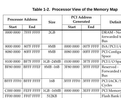
Processor Memory Space
The system board platform uses the local memory map shown in the following table, by default.
3. This space is used for Direct Mapped PCI Configuration Space accesses. Refer to the Direct Mapped PCI Configuration Space section for more details.
4. Flash decoding repeats every 1MB for this entire 16MB range.
5. Using this address range for Flash is not recommended since future PowerPC products will redefine this 14MB area.
6. The M48T18 RTC and NVRAM device is mapped in this area. Refer to the ISA I/O Space Mapping section for more details.
CH5-Product Description and Memory Maps
1
Notes 1. All ISA I/O locations not specified in this table are user-definable.
2. These locations are internally decoded by the PIB.
3. These locations are internally decoded by the SIO. 4. These locations are undefined.
0832 8000 0832 8004 1012 Audio: Status Register
0833 8000 0833 8004 1013 Audio: PIO Data Register
0C01 8000 0C01 8006 0001 PIB: Test Mode Control Port/ Shadow Register of Port 70
2, 4
0C04 8000 0C04 8006 0004 PIB: Power Control Output Port
2, 4
Table 1-4. ISA I/O Space Map (Continued)
ISA I/O Address
Processor Address
Function Notes
Note This space does not appear on the processor bus, but instead appears on the memory bus.
PCI Address
Size
Processor Bus
Address DeÞnition
Start End Start End
0000 0000 00FF FFFF 16MB Not forwarded to MPU bus
PCI/ISA Memory Space
0100 0000 7FFF FFFF 2GB -16MB Not forwarded to MPU bus
PCI Memory Space
8000 0000 FFFF FFFF 2GB 0000 0000 7FFF FFFF (see Note)
Onboard DRAM (via MPC105)
0000 0000 FFFF FFFF 4GB Not forwarded to MPU bus
Note Default configuration in the PIB; changeable by software.
Priority (Note) DMA Channel Size Peripheral
Highest 0 8 bit
-1 8 bit
-2 8 bit Floppy Disk
3 8 bit Parallel Port
4 16 bit (not available) 5 16 bit IDE Interface 6 16 bit Audio Playback
Product Description and Memory Maps
Configuration Register, the Power-Down Control Register, the NVRAM/RTC Address Registers (STB0 and STB1), and the NVRAM/RTC Data Port Register. These registers are all accessible in ISA I/O space.
Control and Status Registers (CSRs)
2
CPU Type Register
This register contains the board ID code and the size of the cache memory on the system board platform.
ID (Board) ID. These four bits encode the system board
platform ID code. The current ID is 4.
CSIZE Cache Size. These bits indicate the amount of cache
memory installed on the cache board on the system board platform. The following chart provides the bit code breakdown for the cache memory size.
REG CPU Type Register - 80000800h (ISA 0800h)
BIT SD07 SD06 SD05 SD04 SD03 SD02 SD01 SD00
FIELD ID CSIZE
OPER R
RESET 0100_00XXb
SD01 SD00 Cache Size
0 0 512K Cache
0 1 256K Cache
1 0 Reserved
TERMPW Termination Power. When set, this bit indicates that the system board platform is supplying power to the SCSI terminators; that is, the termination power has not been overloaded by an external device and has not caused the polyswitch ÒfuseÓ to open. If clear, then the SCSI termination power has been
disconnected due to some sort of overload condition.
Note This bit is undefined if SCSIP- is not low (i.e., a SCSI controller must be installed as well).
IDEP- IDE Present-. When clear, this bit indicates that the
system board platform was constructed with an IDE disk controller installed. If set, then no IDE
controller was installed.
AUDP- Audio Present-. When clear, this bit indicates that
the system board platform was constructed with an audio controller installed. If set, then no audio controller was installed.
BIT SD07 SD06 SD05 SD04 SD03 SD02 SD01 SD00
FIELD TERM
PW
IDEP- AUDP- BUS2X- TEST- GFXP- NETP-
SCSIP-OPER R
Control and Status Registers (CSRs)
2
BUS2X- Bus Speed 2X-platform was constructed with a bus speed 2X that . When this bit is set, the system boardof the clock (e.g., a 33 MHz system clock and a 66 MHz bus clock); otherwise, the system clock and the bus clock are the same frequency. This bit is used to help system software determine the type of system board platform it is running upon.
TEST- Test-. When this bit is clear, the firmware is expected
to run diagnostics upon startup. If set, normal operation should occur. This bit should normally be set.
GFXP- Graphics Present-. When clear, this bit indicates that
the system board platform was constructed with a graphics controller installed. If set, then no graphics controller was installed.
NETP- Networking Present-. When clear, this bit indicates
that the system board platform was constructed with a network controller installed. If set, then no network controller was installed.
SCSIP- SCSI Present-. When clear, this bit indicates that the
SPEEDB Speed ÒBÓ. These two bits encode the speed of the DRAM SIMMs installed in group ÒBÓ (the second set), and applies to the SIMM pair. By decoding these bits using the following chart, the speed of the installed SIMMs may be detected.
Note The system board platform does not detect 100ns SIMMs; it will assume they are 50 ns. The use of 100 ns SIMMs will most likely cause the system to fail or to work unreliably. DO NOT USE 100 ns SIMMs.
BIT SD07 SD06 SD05 SD04 SD03 SD02 SD01 SD00
FIELD SIZEB SPEEDB SIZEA SPEEDA
OPER R
RESET 00h
MSB LSB Speed
0 0 50 ns / 100 ns
1 0 80 ns
0 1 70 ns
Control and Status Registers (CSRs)
2
SIZEB Size ÒBÓDRAM SIMMs installed in group ÒBÓ (the second . These two bits encode the size of theset), and applies to the SIMM pair. By decoding these bits using the following chart, the size of the installed SIMMs may be detected.
Note that the size encodings are not unique for each possible part; the values do provide useful hints as to the expected size, but software is expected to resolve the remaining differences.
SPEEDA Speed ÒAÓ. These two bits encode the speed of the
DRAM SIMMs installed in group ÒAÓ (the first set), and applies to the SIMM pair. By decoding these bits using the table as described in the SPEEDB section, the speed of the installed SIMMs may be detected.
SIZEA Size ÒAÓ. These two bits encode the size of the
DRAM SIMMs installed in group ÒAÓ (the first set), and applies to the SIMM pair. By decoding these bits using the table as described in the SIZEB section, the size of the installed SIMMs may be detected.
MSB LSB SIMM Size (bytes)
0 0 4MB, 64MB
1 0 32MB
0 1 16MB
RSPDN RS-232 Driver Power-down. When set, this bit indicates that the RS-232 drivers for the serial ports should be powered down; if clear, the drivers are powered up. This bit controls a power converter, so a few milliseconds should elapse between activating the power and attempting to use the serial I/Os.
AMPDN Amplifier Power-down. When set, this bit indicates
that the audio speaker amplifier (for the internal speaker) should be disabled. If clear, then audio signals sent to the amplifier will be driven to the speaker.
AUDDN Audio Power-down. When set, this bit indicates that
the audio CODEC should be powered down. If clear, the audio CODEC will be made active.
IODN I/O Controller Power-down. When set, this bit
indicates that the audio ÒSuperÓ I/O controller should be powered down. If clear, the controller will be made active.
REG Power-Down Control Register - 80000807h (ISA 0807h)
BIT SD07 SD06 SD05 SD04 SD03 SD02 SD01 SD00
FIELD RSPDN AMP
DN
AUD DN
IODN
TERM-OPER W
Control and Status Registers (CSRs)
2
TERM- Terminationsystem board platform should enable the on-board . When clear, this bit indicates that theSCSI terminators. If set, the internal terminators are disabled and the external SCSI termination must be used.
NVRAM/RTC Address STB0 Register
NVRAM/RTC Address STB1 Register
REG NVRAM/RTC Address STB0 Register - 80000074h (ISA 0074h)
BIT SD07 SD06 SD05 SD04 SD03 SD02 SD01 SD00
FIELD A7 A6 A5 A4 A3 A2 A1 A0
OPER W
RESET 00h
REG NVRAM/RTC Address STB1 Register - 80000075h (ISA 0075h)
BIT SD07 SD06 SD05 SD04 SD03 SD02 SD01 SD00
FIELD A15 A14 A13 A12 A11 A10 A9 A8
OPER W
The NVRAM and RTC is accessed through the above three registers. When reading from a NVRAM/RTC location, you must do the following:
1. write the low address (A0-A7) of the NVRAM to the NVRAM/RTC STB0 register,
2. write the high address (A15-A8) of the NVRAM to the NVRAM/RTC STB1 register, and
3. then read the NVRAM/RTC Data Port to fetch the NVRAM/RTC data.
When writing to a NVRAM/RTC location, you must:
1. write the low address (A0-A7) of the NVRAM to the NVRAM/RTC STB0 register,
2. write the high address (A15-A8) of the NVRAM to the NVRAM/RTC STB1 register, and
3. then write to the NVRAM/RTC Data Port for the write transfer to take place.
For the NVRAM/RTC that has only 13 address bits (A0-A12), the high address bits (A13-A15) are ignored.
OPER R/W
Control and Status Registers (CSRs)
product, manuals may be purchased by contacting your local Motorola sales office.
Notes Although not shown in the above list, each Motorola Computer Group manual publication number is suffixed with characters that represent the revision level of the document, such as Ò/xx2Ó (the second revision of a manual); a supplement bears the same number as the manual but has a suffix such as
Ò/xx2A1Ó (the first supplement to the second revision of the manual).
The above documents can be purchased as a set, packaged under part number LK-UB60X.
Table A-1. Motorola Computer Group Documents
Document Title Publication
Number
PPCBug Debugging Package UserÕs Manual (Parts 1 and 2) PPCBUGA1/UM PPCBUGA2/UM
PPC1Bug Diagnostics Manual PPC1DIAA/UM
Ultra 603/Ultra 603e/Ultra 604 Installation and Hardware UserÕs Manual ULMB60XA/IH
Phoenix, Arizona 85022 Telephone: (602) 867-6100
DS1643 Nonvolatile Timekeeping RAM Data Manual Dallas Semiconductor
4401 South Beltwood Parkway Dallas, Texas 75244-3292
DS1643/ DS1643LPM
82378 System I/O (SIO) PCI-to-ISA Bridge Controller Intel Corporation
Literature Sales P.O. Box 7641
Mt. Prospect, Illinois 60056-7641 Telephone: 1-800-548-4725
290473-003
NCR53C810 PCI-SCSI I/O Processor Data Manual NCR Corporation
Microelectronics Products Division 1635 Aeroplaza Drive
Colorado Springs, Colorado 80916 Telephone: (719) 596-5795
NCR Hotline: 1-800-334-5454 FAX: (719) 527-8225
T46923I
NCR 53C8XX Family PCI-SCSI I/O Processors Programming Guide NCR Corporation
Microelectronics Products Division 1635 Aeroplaza Drive
Colorado Springs, Colorado 80916 Telephone: (719) 596-5795
NCR Hotline: 1-800-334-5454 FAX: (719) 527-8225
Table A-3. Related Specifications
Document Title and Source Publication
Number
ANSI Small Computer System Interface-2 (SCSI-2) Global Engineering Documents
15 Inverness Way East Englewood, CO 80112-5704 Telephone: 1-800-854-7179 Telephone: (303) 792-2181
X3.131.1990
ANSI Std X3T9.2, 1994
AT Attachment Interface for Disk Drives Global Engineering Documents 15 Inverness Way East
Englewood, CO 80112-5704 Telephone: 1-800-854-7179 Telephone: (303) 792-2181
ANSI X3.221
Bidirectional Parallel Port Interface SpeciÞcation Institute of Electrical and Electronics Engineers, Inc. Publication and Sales Department
345 East 47th Street
New York, New York 10017-21633 Telephone: 1-800-678-4333
IEEE Standard 1284
IEEE - Common Mezzanine Card SpeciÞcation (CMC) Institute of Electrical and Electronics Engineers, Inc. Publication and Sales Department
345 East 47th Street
New York, New York 10017-21633 Telephone: 1-800-678-4333
11400 Burnet Road Austin, Texas 78758-3493
Related Documentation
10base-2 See thin Ethernet.
10base-T See twisted-pair Ethernet.
ACIA Asynchronous Communications Interface Adapter
AIX Advanced Interactive eXecutive (IBM version of UNIX)
architecture The main overall design in which each individual hardware
component of the computer system is interrelated. The most common uses of this term are 8-bit, 16-bit, or 32-bit
architectural design systems.
ASCII American Standard Code for Information Interchange. This is a 7-bit code used to encode alphanumeric information. In the IBM-compatible world, this is expanded to 8-bits to encode a total of 256 alphanumeric and control characters.
ASIC Application-Specific Integrated Circuit
AUI Attachment Unit Interface
BBRAM Battery Backed-up Random Access Memory
bi-endian Having big-endian and little-endian byte ordering
capability.
big-endian A byte-ordering method in memory where the address n of
G
L
O
S
S
A
R
Y
hardware A computing system is normally spoken of as having two
major components: hardware and software. Hardware is the term used to describe any of the physical embodiments of a computer system, with emphasis on the electronic circuits (the computer) and electromechanical devices (peripherals) that make up the system.
HCT Hardware Conformance Test. A test used to ensure that
both hardware and software conform to the Windows NT interface.
I/O Input/Output
IBC PCI/ISA Bridge Controller
IDE Intelligent Device Expansion
IEEE Institute of Electrical and Electronics Engineers
interlaced A graphics system in which the even scanlines are refreshed
in one vertical cycle (field), and the odd scanlines are refreshed in another vertical cycle. The advantage is that the video bandwidth is roughly half that required for a non-interlaced system of the same resolution. This results in less costly hardware. It also may make it possible to display a resolution that would otherwise be impossible on given hardware. The disadvantage of an interlaced system is flicker, especially when displaying objects that are only a few scanlines high.
IQ Signals Similar to the color difference signals (R-Y), (B-Y) but using
G
L
O
S
S
A
R
Y
SMT Surface Mount Technology. A method of mounting devices
(such as integrated circuits, resistors, capacitors, and others) on a printed circuit board, characterized by not requiring mounting holes. Rather, the devices are soldered to pads on the printed circuit board. Surface-mount devices are typically smaller than the equivalent through-hole devices.
software A computing system is normally spoken of as having two
major components: hardware and software. Software is the term used to describe any single program or group of programs, languages, operating procedures, and
documentation of a computer system. Software is the real interface between the user and the computer.
SRAM Static Random Access Memory
SSBLT Source Synchronous BLock Transfer
standard(s) A set of detailed technical guidelines used as a means of
establishing uniformity in an area of hardware or software development.
SVGA Super Video Graphics Array (IBM). An improved VGA
monitor standard that provides at least 256 simultaneous colors and a screen resolution of 800 x 600 pixels.
Teletext One way broadcast of digital information. The digital
G
L
O
S
S
A
R
Y
VME2PCI MCG ASIC that interfaces between the PCI bus and the
VMEchip2 device.
volatile memory A memory in which the data content is lost when the power
supply is disconnected.
VRAM Video (Dynamic) Random Access Memory. Memory chips
with two ports, one used for random accesses and the other capable of serial accesses. Once the serial port has been initialized (with a transfer cycle), it can operate
independently of the random port. This frees the random port for CPU accesses. The result of adding the serial port is a significantly reduced amount of interference from screen refresh. VRAMs cost more per bit than DRAMs.
Windows NT™ The trademark representing WindowsNew Technology, a computer operating system developed by the Microsoft Corporation.
XGA EXtended Graphics Array. An improved IBM VGA monitor
standard that provides at least 256 simultaneous colors and a screen resolution of 1024 x 768 pixels.
Y Signal Luminance. This determines the brightness of each spot
Glossary