Iranian Journal of Electrical & Electronic Engineering, Vol. 8, No. 3, Sep. 2012 259
Experimental Study and Steady State Stability Analysis of
CLL-T Series Parallel Resonant Converter with Fuzzy
Controller using State Space Analysis
C. Nagarajan
*and M. Madheswaran
**Abstract: This paper presents a Closed Loop control of CLL-T (Capacitor Inductor
Inductor). Series Parallel Resonant Converter (SPRC) has been simulated and the performance is analysised. A three element CLL-T SPRC working under load independent operation (voltage type and current type load) is presented in this paper. The Steady State Stability Analysis of CLL-T SPRC has been developed using State Space Technique and the regulation of output voltage is done by using Fuzzy controller. The simulation study indicates the superiority of fuzzy control over the conventional control methods. The proposed approach is expected to provide better voltage regulation for dynamic load conditions. A prototype 300 W, 100 kHz converter is designed and built to experimentally demonstrate, dynamic and steady state performance for the CLL-T SPRC are compared from the simulation studies.
Keywords: Control System, Fuzzy logic, MATLAB, Power Electronics, Resonant
Converter.
1 Introduction1
The developments of the DC-DC Resonant Converters are increasing now a day due its performance. A DC-DC Resonant Converter (RC) are used in telecommunication and aerospace application, at high frequency these converters experience high switching losses, reduced reliability, electromagnetic interference (EMI) and acoustic noise. To overcome these drawbacks, the SPRC is found to be suitable, due to various inherent advantages. The Series and parallel Resonant Converter (SRC and PRC respectively) circuits are the basic resonant converter topologies with two reactive elements. The merits of SRC include better load efficiency and inherent dc blocking of the isolation transformer due to the series capacitor in the resonant network.
However, the load regulation is poor and output-voltage regulation at no load is not possible by switching frequency variations. On the other hand, PRC offers no-load regulation but suffers from poor load efficiency and lack of dc blocking for the isolation
Iranian Journal of Electrical & Electronic Engineering, 2012. Paper first received 18 Feb. 2011 and in revised form 4 July 2012. * The Author is with the Research Scholar in Bharath University, Chennai. Tamilnadu, India.
E-mail: [email protected].
** The Author is with the Centre for Advanced Research, Muthayammal Engineering College, Rasipuram, Tamilnadu, India.
transformer. It has been suggested to design Resonant Converter with three reactive components for better regulation. The LCL tank circuit based DC-DC SPRC has been experimentally demonstrated and reported by many researchers [1-4]. Mangesh B. Borage et al [5] have demonstrated the characteristics of LCL-T Resonant converter using Asymmetrical duty cycle (ADC). The converter operated at fixed resonant frequency and its analysised using state space approach. Later, Mangesh Borage et al [6] have demonstrated an LCL-T half bridge resonant converter with clamp diodes. The output current or voltage is sensed for every change in load because the output voltage or constant current increases linearly. The feedback control circuit has not been provided. LCL-T RC with constant current supply operated at resonant frequency is presented [7].
Vijayakumar Belaguli et al [8] have experimentally demonstrated with independent load when operated at resonant frequency, making it attractive for application as a constant voltage (CV) power supply. It has been found from the literature that the LCL tank circuit connected in series-parallel with the load and operated in above resonant frequency improves the load efficiency and independent operation. Chew L et al [9] have demonstrated LCC SPRC using robust control method, this method used to varying the converter gain, the gain was derived by using state plan analysis. The voltage and current type load was presented with
variable load condition. The closed loop operation was presented using PI controller with load independent operation as obtained.Lakshminarasamma N. et al [10] have demonstrated active clamp ZVS DC-DC converter. The steady state stability analysis was presented for ZVS Buck converter. There is no possible of load independent operation. The converter operates at duty cycle >0.5, above its operation the converter fails to instability. Later, Martin P.Foster et al [11] have demonstrated CLL half bridge Resonant Converter with open loop operation. The ac equivalent circuit analysis and fundamental mode approximation (FMA) analysis was derived used to the modeling the converter and compared.
Paolo Mattavelli et al [12] have demonstrated different approaches which offer the fuzzy logic control (FLC). This control technique relies on the human capability to understand the system’s behavior and is based on qualitative control rules. The FLC approach with same control rules can be applied to several dc–dc converters. The author utilized the proposed control technique for Buck-Boost converter and demonstrated. J.M. Correa et al [13] have demonstrated a DC/AC series resonant converter with fixed load value considering two control approaches.
Later T. S. Sivakumaran et al [14] have demonstrated a CLC SPRC using FLC for load regulation and line regulation. The performance of controller has been evaluated and found that the load independent operation may not be possible. C.Nagarajan et al [15] have simulated an LCL-T SPRC using FLC and PID controller. The performance of controller has been found to be better when the fuzzy controller has been considered. The Harmonic Spectrum and dynamic analysis for RLE load are presented. M.Prabhakar et al [16] have simulated an LCC RC. The closed form expressions are derived for different resonant topologies. The Voltage gain expression for these topologies are obtained and plotted.
It is clear from the above literatures that the output voltage regulation of the converter against load and supply voltage fluctuations have important role in designing high-density power supplies. A CLL-T SPRC is expected the speed of response, voltage regulation and better load independent operation. Keep the above facts in view, the CLL-T SPRC has been model and analysised for estimating various responses. The closed loop state space model and AC analysis has been derived and simulate using MATLAB/Simulink. A prototype 300 W, 100 kHz the CLL-T SPRC is implemented and the experiment results are compared with the simulation results. The simulation results agree with the experimental results.
2 Proposed CLL-T Series Parallel Resonant Converter with Fuzzy Controller
The resonant tank consisting of three reactive energy storage elements (CLL-T) has overcome the
conventional resonant converter that has only two reactive energy storage elements. The first stage converts a DC voltage to a high frequency ac voltage. The second stage of the converter is to convert the AC power to DC power by suitable high frequency rectifier and filter circuit. Power from the resonant circuit is taken either through a transformer in series with the resonant circuit or series in the capacitor comprising the resonant circuit as shown in Fig. 1. In both cases the high frequency feature of the link allows the use of a high frequency transformer to provide voltage transformation and ohmic isolation between the DC source and the load.
In CLL-T SPRC the load voltage can be controlled by varying the switching frequency or by varying the phase difference between the two inverts where the switching frequency of each is fixed to the resonant frequency. The phase domain control scheme is suitable for wide variation of load condition because the output voltage is independent of load. The DC current is absent in the primary side of the transformer, there is no possibility of current balancing. Another advantage of this circuit is that the device currents are proportional to load current. This increases the efficiency of the converter at light loads to some extent because the device losses also decrease with the load current. If the load gets short at this condition, very large current would flow through the circuit. This may damage the switching devices. To make the circuit short circuit proof, the operating frequency should be changed.
A schematic diagram of full-bridge CLL-T SPRC is shown in Fig. 2. The resonant circuit consist of series inductance L1, parallel capacitor C and series inductance
L2. S1-S4 is switching devices having base /gate turn-on
and turn-off capability. D1 to D4 are anti-parallel diodes
across these switching devices. The MOSFET (S1) and
its anti parallel diode (D1) act as a bidirectional switch.
The gate pulses for S1 and S2 are in phase but 180
degree out of phase with the gate pulses for S3 and S4.
The positive portion of switch current flows through the MOSFET and negative portion flows through the anti-parallel diode. The RLE load is connected across bridge rectifier via L0 and C0. The voltage across the point AB
is rectified and fed to RLE load through L0 and C0. For
the analysis it is assumed that the converter operates in the continuous conduction mode and the semiconductors have ideal characteristics.
3 Steady State Stability Analysis for the Proposed Converter
3.1 Mathematical Modeling using State Space Technique
The equivalent circuit of CLL-T SPRC is shown in Fig. 3. The mathematical modeling using state space technique can be obtained assuming all the components to be ideal. The state space equation for CLL-T SPRC converter is:
Nagarajan & Fig. 1 Block Converter.
Fig. 2 Circuit
Fig. 3 Equival
1 1
L
V
dt
di
L=
C−
2 2
L V dt
diL = C −
C
i
dt
dV
C=
L1+
The state-spa ⎢ ⎢ ⎢ ⎢ ⎢ ⎢ ⎣ ⎡ + ⎢ ⎢ ⎢ ⎢ ⎢ ⎢ ⎣ ⎡ = ⎥ ⎥ ⎥ ⎦ ⎤ ⎢ ⎢ ⎢ ⎣ ⎡ 2 1 V i i dt d C L L & Madheswara Diagram of C
diagram of CLL
lent Circuit Mo
1
L
V
in−
, 2 0 1 L V L Vin −− ,
C
i
L2+
ace model for
⎣ ⎡ − − − 0 0 2 1 1 1 0 1 1 0 1 1 2 1 0 0 1 1 0 0 L L L C C L L an: Experimen CLL-T Series L-T SPRC.
del of CLL–T S
CLL-T SPRC
( )
( )
( )
⎥ ⎦ ⎤ ⎢ ⎣ ⎡ ⎥ ⎥ ⎥ ⎥ ⎥ ⎥ ⎦ ⎤ ⎥ ⎥ ⎥ ⎦ ⎤ ⎢ ⎢ ⎢ ⎣ ⎡ ⎥ ⎥ ⎥ ⎥ ⎥ ⎥ ⎦ ⎤ 0 2 1 2 1 V V t V t i t i in C L Lntal Study and Parallel Reson SPRC. (1 (2 (3 C:
d Steady State nant 1) 2) 3) (4) fac out Als are squ fun fro fun har tur ass the a R sw r ω net Z =
δ
M by cha the sui M H 4 spe vol the des spe obt rese Stability Ana 3.2 AC An
The converte ctor mode, A
t to bring out so, in the AC e replaced by uare-wave inp ndamental sin om input to o
ndamental com rmonics is ne rn’s ratio (N sumed to be u e rectifier with
o
ac 2 R
8
π
= The resona witching freque , 1 f LC r = The characte twork are and C L =The ratio of i
1 2 L L = The voltage
= and H V V M in o Voltage gain using Eq. (9 aracteristics p e desired cha
itability for au
⎜⎜ ⎝ ⎛ − = = 1 in o V V M ⎠ ⎞ ⎜⎜ ⎝ ⎛ − =
ω
1 1 1 n Q Results and 4.1 DesigFor the des ecifications ar ltage, maximu e full-load con sired to desi ecifications as tained using sonance for al
alysis of CLL-nalysis for the
er is operated C sinusoidal t the importan C analysis, the y the equival
put voltage nusoidal equiv
output is ass mponent and eglected. With N1/N2) of the
unity. The eq h capacitive fi
ant frequenc ency are defin
, 2 1 LC π =
ω
eristics impeda o r R R L Q=ω
=inductance is
and current ga
⎟ ⎠ ⎞ ⎜ ⎝ ⎛ = Z V I H in o
n for the conv 9), from the v plot is obtaine aracteristics utomotive app + ⎟⎟ ⎠ ⎞
π
ω
8 1 2 n Q j ⎜⎜ ⎝ ⎛ + ⎟⎟ ⎠⎞
π
δω
8 1 2 n j Discussion gn Parametersign of CLL-re: minimum a um output cur ndition and sw ign the conv s shown in T a design p lmost all pow
T … e Proposed C
only in the la analysis has nt features of e output recti lent ac resista
source is rep valent. The p sumed to be
the contribut hout losing g e isolation tr quivalent AC lter is given b
cy and the ned as
n r s n=
ω
, f =ω
ω
ance and Q o
o
R
Z
defined as
ain are defined
erter topology voltage gain ed. This is co
plot to deci lication.
(
⎜⎜ ⎝ ⎛ −ω
δω
1 11 n n Q
(
)
⎟⎟ ⎠ ⎞ + −δ
ω
1 1 nrs of the Con
-T SPRC [5] and maximum rrent (Io), corr
witching frequ verter with t Table 1. These
procedure to er range (load
261 onverter
agging power been carried f the network. fier and filter ance and the placed by its ower transfer only via the tion of all the generality, the ransformer is resistance for by (5) normalized r s f f
= (6)
f the resonant
(7)
(8)
d as (9)
y is computed expression, a ompared with de upon the
)
⎟⎟ ⎠ ⎞ +δ
(10) (11) nverter], the design m value of DC responding to ency (fs). It is
the following e values were o assure the d-independent r d . r e s r e e e s r ) d t d a h e ) n C o s g e e t
design) and values. To pr to show tha parameter va
4
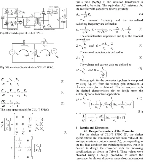
Fuzzy co inference or SPRC are m control is dev variables ‘e’ membership functions are fuzzy rule b intuitive reas NB, NS, Z Negative Sm It can inf reference val (Δu) must b reference val the referenc switching fr voltage is ne rapidly, then to prevent ov At every load voltage change in er FLC. The st defuzzificatio shown in Fig
pe
e
ce
V
V
e
r L−
=
−
=
where Vr is VL is the act
The duty rati fuzzy infere continues to during the c maintain incr A drop in controller to by modifyin
Table 1 Desig S.no 1 Pow 2 Min 3 Min 4 Max 5 Tran 6 Swi 7 Seri 8 Para 9 Loa 10 Loa
also to limit rove the wide at the fuzzy ariations.
4.2 Fuzzy Log
ontrol involve r rule evaluat modeled using
veloped using , ‘ce’ and ‘Δu
functions. e chosen for base created i soning and ex , PS, PB ar mall, Zero, Pos ferred that the lue, then the c be large so a lue quickly. T ce value, an requency is ear the referen n the frequenc
vershoot. sampling inte e are used to rror (ce) signa tage of fuzzi on are then p g. 4.
e
L
the reference tual output vo io of the conv ence. For ins increase grad charging proc rease in voltag n the output v
increase the o ng the Mod
gn Parameters. Parame wer output nimum input vo nimum output v ximum load cur nsformer Turns tching frequenc ies Inductance L allel Capacitanc ad Inductance (L ad Capacitance (
the current a e load range op
controller us
gic Control (F
es three stage tion and defu g MATLAB g the fuzzy to
u’ are describ Five triangu simplicity. Ta in the present xperience. Fuz re defined as sitive Small, a e output voltag
change of swi as to bring th The output vo nd then a sm
necessary an nce value and cy must be ke
erval, the refer o calculate th als that act as ification, fuzz performed as
or the desire oltage and pe i verter can be d stance, if the dually while th cess the fuzzy ge to reach the voltage level t
output voltage dulation Inde eter oltage voltage rrent s ratio
cy (fs)
L1, L2
ce (C) Lo)
(Co)
and voltage p peration and a sed is robust
FLC)
es: fuzzificati uzzification. T
software. Fu olbox. The fu bed by triangu ular members
able 2 shows t work based zzy membersh s Negative B and Positive B
ge is far from itching freque he output to oltage approac mall change nd if the out
is approachin ept constant so
rence voltage he error (e) s the input to zy inference
given flowch
(
d output volta is previous er determined by e output volt he current is y controller w e set point. triggers the fu e of the conve ex (MI) of
Value 300W 100V 100V 3A 1 100KHz 39.18 μH 66 nF 1mH 650μF
peak also t to ion, The uzzy uzzy ular ship the d on hips Big, ig. the ency the ches of tput ng it o as and and the and hart (12) age, rror. y the tage low will uzzy erter the con rel fuz fuz Tab E
Change in error
() usi and sw par MA fre sim loa ind inv imp con by Fig
nverter. The r ies on the fuz zziness of th zziness of thei
ble 2 Fuzzy Ru Error (e) (ce ) NB NB NB NS NB Z NB PS NM PB Z
The Closed l ing MATLAB d the chang witching frequ
rameters instr ATLAB are equency of the mulated with a The resonan ad voltage are ductor and ca verter for re pedance mat nverter is that
the non i
g. 4 Flowchart
resolution of zziness of the he control v ir membership
ules.
B NS Z B NB N B NM N B NS Z M Z P PM PB
4.3 Simulati
loop simulatio B/Simulink sof e in error, uency is ca ruction and fu
used to up e pulse gener a switching fre nt voltage, re
e shown in Fi apacitor are c sonance purp tching. Anoth t the converte idealities of
for the Fuzzy c
fuzzy logic c control variab variables dep p functions.
Z PS P NB NM Z NS Z P Z PS P S PM P B PB P
on Results
on using FLC ftware. Depen the value o lculated. The unction block pdate the ne
ators. The en equency of 10 sonant curren ig. 5(a) and F connected to
pose and it her good fea er operation is the output
controller.
ontrol system bles while the ends on the
PB Z PM PB PB PB
is carried out nding on error of change of e Fuzzy set s available in ew switching ntire system is
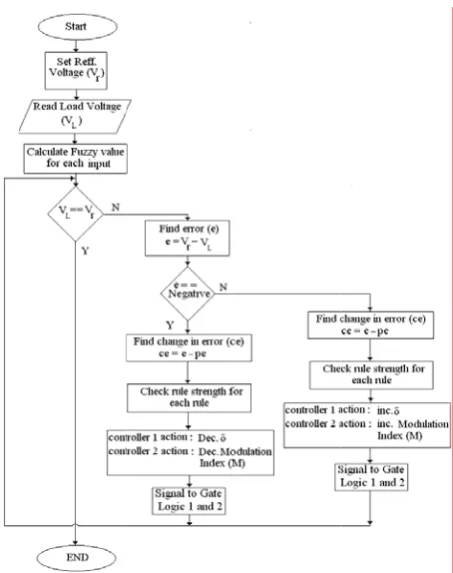
00 KHz. nt and output Fig. 5(e). The the output of is used for ature of this s not affected transformer m e e t r f t n g s t e f r s d r
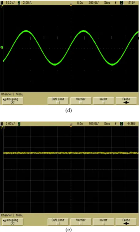
Nagarajan & Fig. 5 (a) I (Transformer Current throu load for Vr=10
& Madheswara Inverter Voltag Primary side), gh Inductance 00V.
an: Experimen (a)
(b)
(c)
(d)
(e)
ge (VAB), (b)
(c) Voltage ac L1, (e) Outpu
ntal Study and Inverter Cur cross Capacitor, ut voltage for R
d Steady State rrent
, (d) RLE
(m res obs in con net out tha
elim noi rea num inf hig con Tab eff tab the stra
4
con the G( pla dir pla sta imp G( rig
sta obs dir Als of
fre and cur cha fre
Ta per
e Stability Ana
magnetizing in sonance induc
served that the the resonant nduction loss twork. The r tput voltage i at of the settlin
It is clear th minating the ise suppressi asons. The i mber, thus m ferred that the ghly suppres
nverter respon ble 3. This en fectively with ble shows tha e settling time
ategy. The me
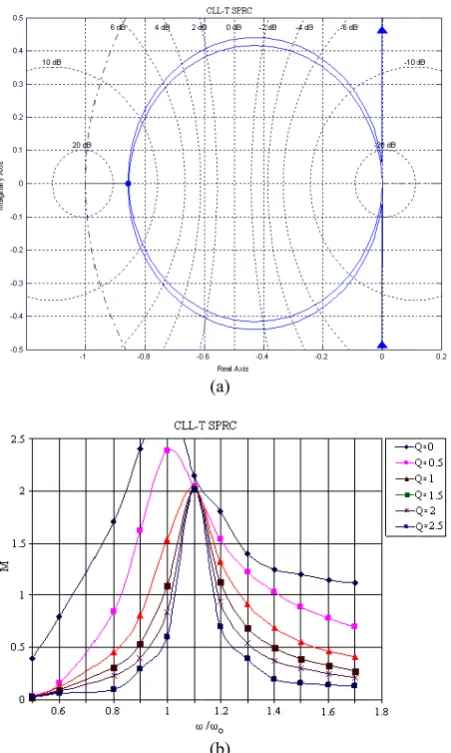
4.4 Stability
Fig. 6(a) rep nverter using e stability is s)H(s) plan c an encircles rection as man an poles of G able. There is pels that the s) H(s) in the ght half s-plan It is conclud able for the
served that rection in one so the open lo s-plan.
4.5 Con
Fig. 6(b) sh equency ratio
d different v rve correspon aracteristics. equency ratio,
able 3 Evalu rformances by u
Controller
Open loop Closed Loop (F
alysis of
CLL-nductance) b ctor L2. The ou
e settling time characteristic es in the bri result is justi in CLL-T SPR ng time.
hat the CLL-overshoot, ris on. This hap integrator inc minimizing th
e measureme ssed. The nse have been nsures that the h feedback. It at the peak ov e is much low easurement no
Studies for t
presents the st the extended n
determined i corresponding
the point -1+ ny times as th G(s)H(s) then
s no encirclem system is stab e right half
s-then the syste ded that the C
system par -1+j0 point e time. Hence oop system ha
nverter Analy Conve
hows the co (ωs /ωr) chara
values of Q(0 nding to Q=
The no load transformer t
uation of tra using FLC.
Settl Time
Sec 0.4 FLC) 0.1
T …
ecause of th utput voltage e 0.12 sec. Th cs is due to th
idge inverter ified that sett RC controller
-T SPRC is i se time and hi ppens becaus creases the he steady-stat ent overshoot
performance n estimated an e system can t is clear fro vershoot is el wer with the oise is highly s
he Proposed
tability invest nyquist functi f G(s)H(s) co g to nyquist
+j0 in the a he number of the closed lo ment of -1+j0 ble if there ar -plan. If there em is unstable CLL-T conve rameters vari is encircled e net encircle as no poles at
ysis for the P erter
onverter gain acteristics for 0,0.5,1,1.5,2
0 represents gain (M) de turns ratio an
ansient and
ling e in c.
% Ov Shoo
45 10 12 08
263
he additional are high, it is e slight droop he increase in and resonant tling time of r is more than
ineffective in igh frequency se of several system type e error. It is and noise is of CLL-T nd provided in be controlled om the above liminated and fuzzy control suppressed.
Converter
igation of the ion technique. ontour in the contour in s-anti-clockwise f right half s-oop system is 0 point. This re no poles of e are poles on e.
erter circuit is iations. It is in the both ement is zero. the right half
roposed
n (M) versus r δ=1 (L2 /L1)
and 2.5).The the no load pends on the d δ from Fig.
steady state
er ot
Steady state error 0.04 0.004
l s p n t f n
n y l e s s T n d e d l
e . e -e -s s f n
s s h . f
s ) e d e .
6(b), it has b load indepen designed to point, then t small change utilization o decreases the as the load reaches to fr
condition sh network desi Fig. 6(b) of secondar condition ca (4). It is dif form. The g resonant fre approximatio
Fig. 6 (a) Stab versus ωs /ωr f
been observed ndent feature. operate at o the output vo e in operating of the conv e gain value r decrease. Th fr as the load
hould be the ign.
shows the ωs
ry leakage. an be obtained
fficult to expr gain (M) has equency (fr)
on.
bility analysis o for different Q v
that the conv Therefore, if or near the l oltage can be g frequency. T verter compo reaches to hig he Q increase increases. Th worst case
/ωr=1.15 and
The peak g d by using th ress the peak
error at frequ due to th
(a)
(b)
of CLL-T SPR values.
verter exhibits f the converte oad independ controlled b This allows be onents. The gher gain as w e the gain va hus the full l
for the reson
d shows the ef gain at a gi he gain equat k gain in expl uency below he fundamen
RC (b) voltage g
the er is dent by a etter Q well alue load nant ffect iven tion licit the ntal gain 5 CL des gen the the 410 sho of me is (M acr and Fig per the of res tran rel pre con the nea goo ope can goo CL stu exp are the loa Ou abs loa gra loa stra ind app reg cha the nea of inv con exp pow eff rem Experimenta
A CLL-T SP LL-T SPRC i signed. ATM nerate driving e driver IC IR2 e switches in
00 are used fo own in figures the turn on eans of the re shown in F MSO) of Inve ross parallel c d Output volta g. 7. These
rformance of e inverter volt
the bridge i sonant curren nsformer. Fig atively high esented, whic ntroller. Fig. 7 e current con
arly sinusoida od performanc
One can con erating under n be seen tha od accuracy LL-T SPRC is udies. It is pro perimental re e observed to e output volta ad.
The output utput Power sorbed that th ad and as t adually decre ads. It is also
ategy has les dicate that the proach for gulation. As shown aracteristics eoretical curv arly independ the prototype verter to vary t
nditions at 1 perimental ef wer are show ficiency of the mains above 0
al Results
PRC is fabrica is operating MAL microcon
g pulses, these 2110, the IRF the bridge co or the output b s that the pow
switching are sonant operat ig. 7. The M rter voltage, capacitor, Cur
age fed with t e figures sh the controlle age, its measu inverter. Fig. nt, measured g. 7(c) it can
, but an a ch is assured
7(d) it can be ntains low har al shape. Fig. ce of the who nclude that th r load- indepe at the output f and better dy verified by si oved from the esults shows closely match age is seen to
power for v has been sh he power draw the load inc eases and rem
o seen that t ss load Sensit FLC based C DC-DC co
in Figs. are observed e, and the ou dent of load.
is measured the output pow 00 V input D fficiency as wn in Fig. 8(b e prototype is 0.80 for 100-3
ated and tested at 300 W, 1 ntroller 89C5 e pulses are am F840 MOSFET onverter. The
bridge rectifie wer losses in th e maintained tion. The hard Multi storage inverter Cur rrent through i the DC motor how the go r. Fig. 7(b) C ure from the p . 7(b) CH2: on the prim be seen that almost consta
by the prima e seen from th rmonics and 7(e) the figu le design. he controller endent operat follows the re ynamic perfor imulation and e performance
the control c h the theoretic o be nearly in
various input hown in Fig wn decays stee reases the p mains consta the proposed tivity.The res CLL-T SPRC i onvertor out
8(a), 8(b) d to closely utput power i The conversi by varying th wer under diff DC voltage. a function o b).The full loa measured to b 00 W output p
d. A prototype 100 kHz was 51 is used to mplified using Ts are used as diodes MUR er. It’s clearly he occurrence very low by dware module e oscillogram rrent, Voltage inductance L1
r are shown in ood dynamic CH1: presents point A and B presents the mary of the the peaks are ant level is ary converter his figure that it presents a ure shows the
is capable of tion, again, it eference with rmances. The d experimental e Table 4, the characteristics cal values and ndependent of
t power and g. 8(a). It is eply for lower power drawn ant at greater new control sults obtained is an effective tput voltage
the control y match the is seen to be ion efficiency he pulse to the fferent loading The plots of of the output ad conversion be 0.76 and it power. Out of e s o g s R y e y e m e 1 n c s B e e e s r t a e f t h e l e s d f d s r n r l d e e l e e y e g f t n t f
Nagarajan & Madheswaran: Experimental Study and Steady State Stability Analysis of CLL-T … 265
total 40W power loss in the prototype operating at 300W, a major portion (≈20W) is estimated to occur in the MOSFETs and diodes. The rest of losses can be attributed largely to the core and winding loss in transformer and resonant inductor.
(a)
(b)
(c)
(d)
(e)
Fig. 7 Experimental Waveforms for CLL-T SPRC (a) Hardware module (b) CH1: Resonant Voltage [Volt. Scale: 40 V/div.], CH2: Resonant Current [Amp. Scale: 0.5A/div.] (c) Voltage across the Capacitor [Volt. Scale: 20 V/div.] (d) Current through Series Inductor L 1 [Amp. Scale: 0.5A/div.]
(e) Output Capacitor Voltage [Volt. Scale: 50 V/div.].
Table 4 Performance measures of Theoretical & Simulink Results for CLL-T SPRC fed with RLE Load.
Performance measures Simulation
Studies Experimental Studies
Load Voltage in Volts 99.8 94
Load Current in Amps 1.8 2.6
Settling Time in ms 0.01 1.4
% Over Shoot 1 2.1
Steady state error 0.001 2.3
6 Conclusion
The Stability analysis of CLL-T SPRC has been modeled and estimating the performance for various load conditions. This converter with a voltage type load and current type load shows it provides load independent operation. So, the switching power losses
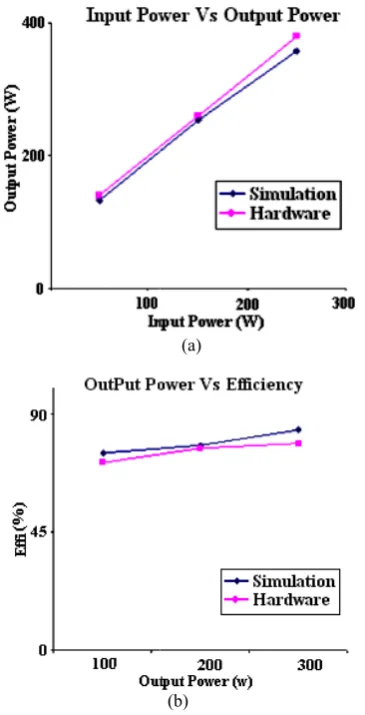
Fig. 8 Experim output power,(
are minimize results that control strat converter wa compared w results agre modeling is e design engin for verity of
References
[1] Bhat A
freque with c
Circui
pp. 97
[2] Raju G
conve simula
Transa
2, pp.
[3] Bhat A
Type
mental results (b) Output Pow
ed. It has be the closed lo tegies. A pr as designed a with the simul ee with the
expected to pr neers for vario
application.
A. K. S., “An ency LCL-Typ capacitive out
its, Devices a
7-103, April 19 G. S. N. and D rter with ation, and
actions on Po
164-174, Mar A. K. S., “A Series Re
(a)
(b)
for (a) input p wer various with
een found fro oop controller rototype 300 and the experi lation results.
experimenta rovide in dept ous converter
nalysis and D pe Series Res tput Filter”, IE and systems,
997.
Doradla S., “A PWM Con Implemen
ower Electron
rch 1995. Analysis and
esonant Con
power various w h Efficiency.
om the simula r provides be 0 W, 100 k iment results . The simulat al results. T th concepts to r design requi
esign of a fix sonant Conve
IEE Preceedin
Vol. 144, N
An LCL Reson ntrol Analy
ntation”, IE
nics, Vol. 10,
Design of LC
nverter”, IE
with
ated etter kHz are tion This the ired
xed-erter
ngs-o.2,
nant ysis,
EEE
No.
CL-EEE
[4]
[5]
[6]
[7]
[8]
[9]
[10
[11
[12
[13
[14
Transacti
No. 1, pp
] Bhat A. K
parallel r
onPower
] Borage M
Tiwari S Asymmet Resonant
Power El
2275, Oct
] Borage M
Resonant
Constant-Industrial
746, Apri
] Borage M
“Analysis Converter
IEEE Tr
Vol. 52, N
] Belaguli
Resonant Current M Experime
Circuits a Applicatio
2000.
] China C.
Control M Converter
Electronic
August 20
0] Lakshmin
Ramanara Current Converter
Electronic
2009.
1] Foster M.
A. and Voltage-O Describin
Power E
1781, July
2] Mattavell
Fuzzy Co
Transacti
1, pp.
79-3] Correa J
Controlle a Series Range”,
Electronic
4] Sivakuma
“Develop Parallel L
ions on Indus
. 118-124, 199 K. S., “Analy resonant conv
r Electron, Vo
M. B., Nagesh S., “Character trical
Duty-Converter”,
lectronics, Vo
t. 2009. M. B., Tiwari S
Converter wi -Current Pow -Voltage Lim
l Electronics,
il 2007. M. B., Tiw s and Design r as a Constan
ransactions o
No. 6, pp. 154
V. and Bhat
Converter O Mode-Analysi ental Results”
and System-I: ons, Vol. 47,
L. and Sng E Method for th
r”, IEEE T
cs, Vol. 24,
009.
narasamma N ayanan V., “ Mode Active
r” IEEE T
cs, Vol. 24, N
. P., Gould C. Bingham C Output Re ng Function
Electronics, V
y 2008. li P. and Spia ontroller for D
ions on Power
-86, Jan. 1997 J. M. and F
d Pulse Densi Resonant In
IEEE Tr cs,Vol. 12, No
aran T. S. pment of Fu
Loaded Reso
strial Electron
94.
ysis and desig verter”, IEEE
ol. 8, pp. 1–11 h K. V., Bhat ristics and D Cycle-Contro
, IEEE Tran
ol. 24, No. 1
S. and Kotaia ith Clamp Dio wer Supply w
it”, IEEE Tra
, Vol. 54, No
wari S. and n of an LCL
nt-Current Po
on Industrial
47-1554, Dec. A. K. S, “S Operating in D
is, Design, Sim ”, IEEE Tra : Fundamenta
No. 4, pp. 43
E. K. K., “A N he Series-Para
Transactions
, No. 8, pp
N., Masihuzza “Steady state e Clamp ZV
Transactions
No. 10, pp. 129
. R., Gilbert A C. M.,“Analy
sonant Conv
”, IEEE Tra
Vol. 23, No.
azzi G., “Gen DC–DC Conv
r Electronics,
.
Farret F. A., ity Modulation nverter with
ransactions
o. 1, pp. 1650 and Natar uzzy Control onant convert
nics, Vol. 44,
gn of a series
Transactions
, Jan. 1993. tia M. S. and Design of an olled LCL-T
nsactions on
10, pp.
2268-ah S., “LCL-T odes: A Novel with Inherent
ansactions on
o. 2, pp.
741-Kotaiah S., L-T Resonant ower Supply”,
Electronics,
2005. Series-Parallel Discontinuous mulation, and
ansactions on al Theory and
33-442, April
Noval Robust allel Resonant
on Power
. 1896-1940,
aman M. and e stability of VS DC-DC
on Power
95-1304, Oct.
A. J., Stone D. ysis of CLL verters using
ansactions on
4, pp.
1772-neral-Purpose verters”, IEEE
, Vol. 12, No.
, “A Fuzzy-n Strategy for Wide Load
on Power
-1655, 2003. rajan S. P.,
l of Series-er-Simulation ,
s
s
d n T
n
-T l t
n
-, t , ,
l s d
n d
l
t t
r
,
d f C
r
.
. L g
n
-e
E
.
-r d
r
, -n
Nagarajan & Madheswaran: Experimental Study and Steady State Stability Analysis of CLL-T … 267
and Experimental Evaluation”, India
International Conference on Power Electronics 2006, pp. 360-366, 2006.
[15] Nagarajan C. and Madheswaran M.,
“Performance Analysis of LCL-T Resonant Converter with Fuzzy / PID Controller Using State Space Analysis”, International Journal of Electronic Engineering Research. Vol. 2, No. 1,
pp. 51-70, 2010.
[16] Prabhakar M., Arulmaozhi S. and Kamaraj V., “Selection Criteria and Analysis of LCC resonant DC-DC Converters for Automotive Application”,
Modern Applied Science, Vol. 3, No. 7, Julyh
2009.
C. Nagarajan received the B.E.
degree from K.S.Rangasamy College of Technology, affiliated to Madras University, during 1997-2001, India, and the M.Tech degree from the Vellore Institute of Technology, Vellore, Tamilnadu India, in 2004. He is currently working towards his doctoral degree at Bharath Institute of Higher Education and Research (BIHER) University, Chennai, India. He has been a member of the faculty at Centre for Advanced Research, Muthayammal Engineering College, Rasipuram, Tamilnadu, India since 2005. His research interests include fuzzy logic and neural network applications to power electronics and drives.
M. Madheswaran received the
BE Degree from Madurai Kamaraj University in 1990, ME Degree from Birla Institute of Technology, Mesra, Ranchi, India in 1992, both in Electronics and Communication Engineering. He obtained his PhD degree in Electronics Engineering from the Institute of Technology, Banaras Hindu University, Varanasi, India, in 1999. At present he is a Principal of Muthayammal Engineering College, Rasipuram, India. He was awarded the Young Scientist Fellowship (YSF) by the State Council for Science and Technology, Tamil Nadu, in 1994 and Senior Research Fellowship (SRF) by the Council of Scientific and Industrial Research (CSIR), Government of India in 1996. Also he has received YSF from SERC, Department of Science and Technology, Govt. of India. He is a life member of IETE, ISTE and IE (India) and also a senior member of IEEE.
![語音增強基於小腦模型控制器(A Speech Enhancement System Based on Cerebellar Model Articulation Controller) [In Chinese]](data:image/gif;base64,R0lGODlhAQABAIAAAP///wAAACH5BAEAAAAALAAAAAABAAEAAAICRAEAOw==)