A THIRD ORDER SIGMA DELTA MODULATOR IN 45nm
CMOS TECHNOLOGY
1
M.SIVA KUMAR, 2SANATH KUMAR TULASI, 3R.ARUNKANTH, 4M.NANDINI,
5
G.SUDHEEER KUMAR
1
ASSOC PROF, K L UNIVERSITY, Department of ECE, ANDHRAPRADESH, INDIA
2
ASST.PROF. K L UNIVERSITY, Department of ECE, ANDHRA PRADESH, INDIA
3, 4, 5 STUDENTS, K L UNIVERSITY, Department of ECE, ANDHRA PRADESH, INDIA
E-mail: [email protected], [email protected], [email protected],
4
[email protected], [email protected]
ABSTRACT
In present communication systems low power ADC’s along with high speed characteristics are the main building blocks. Present the implementation of these ADC architectures are in scaled VLSI technologies. This paper delineates the design of a third order single loop switched Capacitor sigma delta modulator designed of 45nm CMOS technology. The modulator designed is to reduce the power consumption in the low voltage field. The power consumption is dependent on the utilization of OTA. So the Gain enhancement OTA which has more power efficiency compare to two-stage OTA is opted. Simulation results shown are with 45nm CMOS technology with ±1.2V supply voltage. To design Σ-Δ modulator TANNER EDA TOOL is used, the schematic is drafted using S-Edit, analysis of transient response have been done in T-Spice and waveforms are simulated in W-Edit
Keywords: VLSI Technologies, Low-Power Circuits, Sigma Delta Modulator, Switched-Capacitor, Operational Trans conductance, rail-to-rail swing, Class-AB Amplifier.
1. INTRODUCTION
Now-a-days the principle of Σ-Δ
modulation was widely used and developing in recent technologies. Portable hardware devices, similar to personal remote specialized gadgets, computerized cameras, personal audio gadgets, and so forth, are flourishing the markets [2] due to rapid growth in SDM techniques. As driven by batteries, their supply voltage is constrained, and the battery lifetime is huge for these gadgets. Every one of these elements addresses the necessities of low voltage low power designs [3]. Operational Transconductance Amplifiers are the necessary building block in several analog systems. These analog systems usually need low power, quick settling time and high dynamic range The CMOS Operational Trans conductance amplifier (OTA) is an idiosyncratic device with characteristics notably suited to applications viz. multiplexing, amplitude modulation, analog multiplication, gain control, switch circuitry and comparators.
While discussing concerning low-voltage,
low-power ultra deep submicron
technology, sure points of interest will be picked up. Then again, a couple of disadvantages are too
expected. Strained by the semiconductor unit break down voltage, there is low operating voltage in
UDSM technology. Later on the Vth of the
semiconductor unit is in addition less that is worth it to actualize the applications on low voltage. There is no need of especially composed low voltage designs that rearranges the circuits which also brings down the facility utilization. Some analog digital circuits of low power low voltage elaborate to this point are structured in UDSM technology [4].
2. BUILDING BLOCKS
2.1 Operational Transconductance Amplifier Low voltage analog circuit has increasing its
importance day by day. Especially large
components demands low power consumption. The transconductance amplifier constitutes the basic block of the sigma delta modulator .To determine the modulator’s power consumption OTA performs the basic logic. The consumption of power can be reduced by minimizing the supply voltage along with gate oxide thickness [9]. The OTA is the one which is suited for many applications i.e.
multiplexing, amplitude modulation, analog
multiplication, gain control etc. To implement a low-voltage low-power definitely an OTA topology that provides the rail to rail swing is needed. In CMOS technology, because of the low output impedance the voltage gain is also low. To increase the voltage gain the usage of cascading transistors is prohibited. The proposed solution to overcome the problem was to use two stage or multistage topologies as shown in fig. 2 because single stage amplifiers typically have to trade off gain and swing gain. Multi stage amplifiers allow for higher gain without sacrificing swing range. We need extra compensation to establish the closed-loop stability. The current from miller OTA is
(1) Finally the miller OTA current of the miller is given by
(2) The current of the single stage OTA by considering same GBW and the load capacitance is given by
(3)
The above equation explains only the telescopic cascode OTA, there will be two another current branches for the folded cascade amplifier having same current for the two branches and equation is given as
(4)
Fig.1. Two Stages OTA
Fig.2. Current Mirror single stage OTA with gain enhancement
It is clearly observed that for the similar condition, power efficiency is more for the single stage OTA than the explained two staged OTA, because there is no greater power consumption in providing the conductance in the single stage OTA. We can conclude from the above discussions, that it is highly preferred to use single-stage OTA to maintain efficient power. Current mirror OTA of the single stage is the efficient topology. The gain drawn from the current mirror OTA will be around 20-40 dB in CMOS technologies [10]. But we need the gain around 10-20dB so we prefer gain enhancement and it also does not have any extra Here it is contemplated the class-AB amplifier at The output stage because the power efficiency is more than the class A amplifier output stage and it is shown in fig. 3 [18].
Fig.3. Gain enhanced current mirror OTA
It is very important to have Common feedback for differential circuits. So, we preferred a
switched-capacitor Common-Mode Feedback
is a design of single-stage and also consumption of power can be reduced efficiently.
2.2 Comparator and latch
A comparator associated with SET-RESET latch, shown in Fig. 4.The parasitic conductance of the nodes shown are charged to Vdd once the clock given as C1 is low. Within the same means the parasitic conductance of the shown nodes are discharged by transistors once the C1 is high. Comparator designed is pure dynamic logic, and additionally terribly power economical. To design a single-loop Σ-Δ modulator, the necessity for comparator is extremely low as a result of within the single-bit the noise is largely suppressed. By matching the input transistors, offset voltage can be clearly explained [7].
Fig.4. Comparator and Latch
2.3 Switch Circuits
In this Schematic all switches are designed using transmission gates. It's not necessary using boot strapping circuit for boosting the driving voltage as a result of the circuit functioning on its supply voltage. There are 2 easy inverters which are used in driving the switch transistors as given in fig.6. Mostly driving voltage is the voltage which is supplied. Therefore within the whole circuit no node is connected to the voltage which is higher compare to the supply voltage or lower than the ground that most essential for the operation of the circuit [5].
Fig.5.Switch implementation and the local driver
2.4 Clock Generator
The On-chip clock generator is employed in this circuit which is shown in fig 6. The external clock signal is buffered so two non-overlapping clock signals are generated. To eliminate the signal dependent which were delayed are designed.
Fig.6. Clock generator
3. IMPLEMENTATION
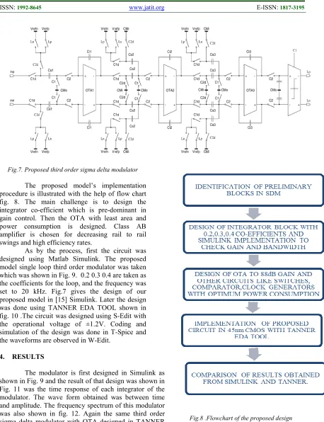
Fig.7. Proposed third order sigma delta modulator
The proposed model’s implementation procedure is illustrated with the help of flow chart fig. 8. The main challenge is to design the integrator co-efficient which is pre-dominant in gain control. Then the OTA with least area and power consumption is designed. Class AB amplifier is chosen for decreasing rail to rail swings and high efficiency rates.
As by the process, first the circuit was designed using Matlab Simulink. The proposed model single loop third order modulator was taken which was shown in Fig. 9. 0.2 0.3 0.4 are taken as the coefficients for the loop, and the frequency was set to 20 kHz. Fig.7 gives the design of our proposed model in [15] Simulink. Later the design was done using TANNER EDA TOOL shown in fig. 10 .The circuit was designed using S-Edit with the operational voltage of ±1.2V. Coding and simulation of the design was done in T-Spice and the waveforms are observed in W-Edit.
4. RESULTS
The modulator is first designed in Simulink as shown in Fig. 9 and the result of that design was shown in Fig. 11 was the time response of each integrator of the modulator. The wave form obtained was between time and amplitude. The frequency spectrum of this modulator was also shown in fig. 12. Again the same third order sigma delta modulator with OTA designed in TANNER EDA TOOL as shown in Fig. 10 and the results of the W-Edit are shown in Fig. 13.The main objective of this project was to reduce the power consumption the design was done in 45nm technology.
Fig.9.Simulink model of 3rd order SDM
As explained before Fig.9 was the Simulink design with the input DSP signal which is analog in nature. As the design was third-order sigma delta modulator three integrators with different coefficients was implemented. The three coefficients were [0.2 0.3 0.4]. Outputs were taken from different blocks i.e. after the comparator which was the final output and from the each integrator for the analysis purpose. A spectrum analyzer was also considered for the frequency response results.
Fig.10.S-Edit Implementation of 3rd order SDM.
Fig.10. explaines the design SDM using Tanner tool. As it was explained before, to design a SDM we need different building blocks which were already shown. By combining those
the circuit diagram was shown in Fig.7. Connections were made according to that proposed circuit diagram. Firstly a switch, clock generator and a feedback circuit were connected to the input, to this OTA was connected. OTA choosen here was the efficient amplifier for the SDM. And the same circuit was implemented thrice as the proposed method was the tird order SDM. To the last OTA a comparator was connected which was a SR latched and the output was connected to that comparator.
Fig.11. Time response of each integrator block
input signal which is a analog input. The next two graphs were the outputs of each integrator where the signal gets integrated after each integrator and it was clearly shown in fig.11. The last graph was the digital output from the comparator as well as from the third integrator according to the connections from fig.9. The last graph was the required digital output for the analog-to-digital conversion. These graphs clearly explains how signal gets integrated as each level and also the requied output.
Fig.12.Output spectrum of proposed topology with 20 kHz input signal.
[image:6.612.335.537.290.435.2]In the proposed simulink design which was shown in fig.9 output sectrum was also connected for the frequency analysis. The above graph was the output frequency spectrum for the proposed topology. The graph was between frequency and time. The input frequency given was 20kHz and the gain obtained was 88dB.
Fig. 13. W-Edit result for Proposed model.
As the proposed method was the CMOS implementation which was designed using
tanner tool. The above figure shows the w-edit result of the tanner. The graph was between the time and amplitude. The figure shows different graphs where the first two were the input waveforms of the sigma delta modulator, the third was the clock signal, fourth was the feedback waveform, fifth was the voltage applied and the last two were the output waveforms of the SDM. All the different graphs were shown in a single figure. The output graph obtained with some noise-distortion where further noise-shaping is required. As it was before the gain was 88dB. Delta-sigma ADCs implement oversampling, decimation filtering, and quantization noise shaping to achieve high resolution and excellent antialiasing filtering
Fig. 14 Multi order sigma delta noise shapes
The noise shaping function in a Σ−∆ modulator is the inverse of the transfer function of the filter in the forward path of the modulator. A filter with higher gain at low frequencies is expected to provide better baseband attenuation for the noise signal. Therefore, modulators with more than one Σ−∆ loop such as the third-order system shown in Figure 9, perform a higher order difference operation of the error produced by the quantizer and thus stronger attenuation at low frequencies for the quantization noise signal. The noise shaping functions of second-order and thirdsecond-order modulators are compared to that of a first-order system in Figure 14. The baseband quantization error power for the third-order system is clearly smaller than for the first-order modulator.
[image:6.612.90.290.527.681.2]transmission channel bandwidth is quite small for delta modulation compared to PCM. The transmitter and the receiver implementation are very much simple for delta modulation. There is no analog to digital converter required in delta modulation.The Demerits of Delta modulation has two major drawbacks that are Slope overload distortion and Granular noise.
5.CONCLUSION
A Switched-Capacitor Sigma Delta
Modulator was designed in 45nm CMOS technology by using TANNER EDA TOOL. The design is also done in Simulink for the frequency analysis and the results were also shown. A proper selection of OTA topology was also done and also designed as explained above. We can also say that UDSM technology have advantages in the implementing the low- voltage low-power sigma
delta modulator than the other CMOS technology. Σ−∆ converters are inherently linear and
don’t suffer from appreciable differential non-linearity,And the background noise level which sets the system S/N ratio is independent of the input signal level. The last, but certainly not least, consideration is cost. Attaining a high level of performance at a fraction of the cost of hybrid and modular designs is probably the greatest advantage of all.
Further this work can be extended to sophisticated 10nm technology or even with CNFETS because of its compactness and low power profiles. The overall gain of the SDM plays a decisive role in figure of merit of the modulator by improving the Operation Trans-Conductance amplifier characteristics we can achieve even better throughput. The gain of Class-AB amplifier is constrained than class D or high gain band width amplifier is recommended.
REFERENCES
[1]S. Loeda, J. Harrison, F. Pourchet, and A.
Adams, “A 10/20/30/40 MHz Feedforward FIR DAC Continuous-Time Delta Sigma ADC With Robust Blocker Performance for Radio Receivers,” IEEE J. Solid-State Circuits,vol. 51, no. 4, pp. 860–870, April 2016.
[2] D. Vercaemer and P. Rombouts, “Analyzing
the Effect of Clock Jitter on Self-Oscillating Sigma Delta Modulators,” IEEE Trans. Circuits Syst.-I Regular Papers, vol. 63, no. 2, pp. 200–210, Feb 2016.
[3] C. Li, R. Hu, H.B. Li, M. Luo, Q. Yang and
S.H. Yu.” Digital OFDM-PON Based on Delta-sigma Modulation Employing Binary IM-DD Channels” IEEE Photonics Journal
Citation information: DOI
10.1109/JPHOT.2016.
[4] Y. Zhang, C.-H. Chen, T. He, and G. C.
Temes, “A Continuous-Time Delta-Sigma
Modulator for Biomedical Ultrasound
Beamformer Using Digital ELD Compensation and FIR Feedback,” IEEE Trans. Circuits Syst.-I: Regular Papers, vol. 62, no. 7, pp. 1689–1698, 2015.
[5] A. Sukumaran and S. Pavan, “Low Power
Design Techniques for Single- Bit Audio Continuous-Time Delta Sigma ADCs Using FIR Feedback.” IEEE J. Solid-State Circuits, vol. 49, no. 11, pp. 2515–2525, Nov. 2014.
[6] R. S. Rajan and S. Pavan, “Design Techniques
for Continuous-Time Delta Sigma Modulators With Embedded Active Filtering,” IEEE J. Solid-State Circuits, vol. 49, no. 10, pp. 2187– 2198, Oct. 2014.
[7] Nizar Khitouni “First order sigma delta
modulator with low-power consumption
implemented in ams 0.35µM CMOS
technology”, IJRET (International Journal of Research in Engineering and Technology, Vol: 02, Issue: 04, Apr-2013.
[8] Radwene Laajimi “First Order Sigma-Delta
Modulator with Low-Power Consumption Implemented In Ams 0.35 mm CMOS Technology” International Journal of Research in Engineering and Technology ISSN: 2319-1163 Volume: 02 Issue: 04 | Apr-2013.
[9] Mohammed Arifuddin Sohel, K. Chenna
Kesava Reddy, Syed Abdul Sattar, “Design of low power sigma delta ADC” , International journal of VLSI design & Communication Systems(VLSICS), Vol.3,No.4,August 2012.
[10]P. Woestyn, P. Rombouts, X. Xing, and G.
[11]Dragos Ducu, Anca Manolescu. “A Continuous Time Sigma Delta Modulator with
Operational Floating Integrator.” INSPEC
Accession Number: 13220449 Semiconductor
Conferences (CAS), 2012.
[12]Liu Yuyu, Yang, Xiaodong, Gao
Jun.”24-bit Low-Power Low-Cost Digital Audio Sigma-Delta DAC” Tsinghua Science and
Technology ISSNl l1007-0214l l12/17l
lpp74-82 Volume 16, Number 1, February
2011.
[13] B. De Vuyst, P. Rombouts, and G. Gielen, “A
Rigorous Approach to the Robust Design of Continuous-Time Sigma Delta Modulators,” IEEE Trans. Circuits Syst.-I, vol. 58, no. 12, pp. 2829–2837, Dec 2011.
[14]Mohammed Arifuddin Sohel, Dr. K. Chenna
Kesava Reddy, Dr. Syed Abdul Sattar. “12 Bit Third Order Continuous Time Low Pass Sigma Delta Modulator for Audio Applications,” ISSN: 2230-7109 (Online) | ISSN: 2230-9543 (Print) IJECT Vol. 2, Issue 4, Oct. - Dec. 2011.
[15]B. De Vuyst and P. Rombouts, “A 5-MHz
11-Bit Self-Oscillating Sigma Delta Modulator With a Delay-Based Phase Shifter in 0.025 mm2,” IEEE J. Solid-State Circuits, vol. 46, no. 8, pp. 1919–1927, Aug. 2011.
[16] E. Prefasi, S. Paton, and L. Hernandez, “A 7
mW 20 MHz BW Time-Encoding
Oversampling Converter Implemented in a 0.08 mm (2) 65nm CMOS Circuit,” IEEE J. Solid-State Circuits, vol. 46, no. 7, SI, pp.1562–1574, Jul. 2011.
[17]B. De Vuyst, P. Rombouts, J. De Maeyer, and
G. Gielen, “The Nyquist Criterion: A Useful Tool for the Robust Design of Continuous-Time Modulators,” IEEE Trans. Circuits Syst.-II, vol. 57, no. 6, pp. 416 –420, June 2010.
[18]R. Jacob Baker “CMOS Circuit Design,
Layout, and Simulation.” Third Edition IEEE Press Series on Microelectronic Systems.
[19]R. Jacob Baker “CMOS Mixed-Signal Circuit