N A N O E X P R E S S
Open Access
Resistive phase transition of the
superconducting Si(111)-(
√
7
×
√
3)-In surface
Takashi Uchihashi
*, Puneet Mishra and Tomonobu Nakayama
Abstract
Recently, superconductivity was found on semiconductor surface reconstructions induced by metal adatoms, promising a new field of research where superconductors can be studied from the atomic level. Here we measure the electron transport properties of the Si(111)-(√7×√3)-In surface near the resistive phase transition and analyze the data in terms of theories of two-dimensional (2D) superconductors. In the normal state, the sheet resistances (2D resistivities)Rof the samples decrease significantly between 20 and 5 K, suggesting the importance of the electron-electron scattering in electron transport phenomena. The decrease inRis progressively accelerated just above the transition temperature (Tc) due to the direct (Aslamazov-Larkin term) and the indirect (Maki-Thompson term) superconducting fluctuation effects. A minute but finite resistance tail is found belowTcdown to the lowest temperature of 1.8 K, which may be ascribed to a dissipation due to free vortex flow. The present study lays the ground for a future research aiming to find new superconductors in this class of materials.
Keywords: Surface reconstruction, Silicon, Indium, Superconductivity, Electron transport, Fluctuation effects, Vortex flow
Background
Semiconductor surface reconstructions induced by metal adatoms constitute a class of two-dimensional (2D) mate-rials with an immense variety [1,2]. They are considered one form of atomic layer materials which can possess novel electronic properties and device applications [3,4]. Recently, superconductivity was measured by scanning tunneling microscopy (STM) for atomically thin Pb films [5,6] and three kinds of Si(111) surface reconstructions: SIC-Pb, (√7×√3)-Pb, and (√7×√3)-In [7]. This dis-covery was followed by a demonstration of macroscopic superconducting currents on Si(111)-(√7 × √3)-In by direct electron transport measurements [8]. These find-ings are important because they enable us to create super-conductors from the atomic level using state-of-the-art nanotechnology. In addition, the space inversion symme-try breaking due to the presence of surface naturally leads to the Rashba spin splitting [9,10] and may consequently help realize exotic superconductors [11].
*Correspondence: [email protected]
International Center for Materials Nanoarchitectonics (MANA), National Institute for Materials Science (NIMS), 1–1, Namiki, Tsukuba, Ibaraki 305–0044, Japan
In reference[8], we have unambiguously clarified the presence of Si(111)-(√7×√3)-In (referred to as (√7× √
3)-In here) superconductivity. However, systematic analysis on electron transport properties above and below the transition temperature (Tc) is still lacking. For
exam-ple, 2D superconductors are known to exhibit the pre-cursor of phase transition due to the thermal fluctuation effects just aboveTc[12-14]. Superconductivity is
estab-lished belowTc, but vortices can be thermally excited in
a 2D system. Their possible motions can cause the phase fluctuation and limit the ideal superconducting property of perfect zero resistance [15]. These fundamental proper-ties should be revealed before one proceeds to search for new superconductors in this class of 2D materials.
In this paper, the resistive phase transition of the (√7× √
3)-In surface is studied in detail for a series of samples. In the normal state, the sheet resistances (2D resistivities)
Rof the samples decrease significantly between 20 and 5 K, which amounts to 5% to 15% of the residual resis-tivityRn,res. Their characteristic temperature dependence suggests the importance of electron-electron scattering in electron transport phenomena, which are generally
marginal for conventional metal thin films. Tc is
deter-mined to be 2.64 to 2.99 K and is found to poorly cor-relate with Rn,res. The decrease in R is progressively accelerated just above Tc due to the superconducting
fluctuation effects. Quantitative analysis indicates the par-allel contributions of fluctuating Cooper pairs due to the direct (Aslamazov-Larkin term) and the indirect (Maki-Thompson term) effects. A minute but finite resistance tail is found belowTcdown to the lowest temperature of
1.8 K, which may be ascribed to a dissipation due to free vortex flow.
Methods
The experimental method basically follows the procedure described in reference [8] but includes some modifica-tions. The whole procedure from the sample preparation through the transport measurement was performed in a home-built ultrahigh vacuum (UHV) apparatus without breaking vacuum (see Figure 1a) [16,17]. First, the (√7× √
3)-In surface was prepared by thermal evaporation of In onto a clean Si(111) substrate, followed by annealing at around 300°C for approximately 10 s in UHV [18-20], and was subsequently confirmed by low-energy electron diffraction and STM. The sample was then patterned by Ar+ sputtering through a shadow mask to define the current path for four-terminal resistance measurements. Typical STM images before and after sputtering are dis-played in Figure 1b,c, respectively. The former shows a clear periodic structure corresponding to the √7×√3 unit cell, while the latter shows a disordered bare silicon surface.
We note that, although the nominal coverage of the evaporated In is more than several monolayers (ML), post annealing removes surplus In layers and establishes the (√7 × √3)-In surface. The In coverage of this surface reconstruction was originally proposed to be 1 ML for the ‘hexagonal’ phase ((√7×√3)-In-hex) and 1.2 ML for the ‘rectangular’ phase ((√7×√3)-In-rect) [18], where 1 ML corresponds to the areal density of the top-layer Si atoms of the ideal Si(111) surface. However, recent theoretical studies point to the coverages of 1.2 ML for the (√7×√ 3)-In-hex and of 2.4 ML for the (√7×√3)-In-rect [21,22]. For our experiments, the dominant phase is likely to be the (√7×√3)-In-hex judging from the resemblance of the obtained STM images (Figure 1b) to the simulated image of the (√7×√3)-In-hex (Figure two, panel b in [22]). The relation between the surface structure and the supercon-ducting properties is intriguing and will be the subject of future work.
In the previous study, van der Pauw’s measurement was adopted to check the anisotropy of electron conduction and to exclude the possibility of spurious supercurrents. In this setup, however, transport characteristics should be analyzed with care because the spatial distribution of bias
current is not uniform. To circumvent this problem, in the present study, we adopted a configuration with a linear current path between the voltage terminals (Figure 1d). The black regions represent the area sputtered by Ar+ ions through the shadow mask. The figure also shows the current density distribution calculated by the finite element method in color scale, which confirms that it is homogeneous between the voltage probes. This allows us to determine the sheet resistanceR of the sample in a more straightforward way:R = (V/I)×(W/L), where
V is the measured voltage,I is the bias current, W =
0.3 mm is the width of the current path, and L = 1.2 mm is the distance between the voltage probes. Figure 1e shows the optical microscope image of a sample, con-firming the clear boundary between the shadow-masked and sputtered regions. Although the sputtering was very light, the resulting atomic-scale surface roughening was enough to make an optical contrast between the two regions.
Following the sample preparation, four Au-coated spring probes were brought into contact with the cur-rent/voltage terminal patterns in a UHV-compatible cryo-stat. Four-terminal zero bias sheet resistance R was measured with a DC bias currentI = 1 μA, and the off-set voltage was removed by inverting the bias polarity. To access the electron conduction only through the (√7 × √
3)-In surface at low temperatures, Si(111) substrates without intentional doping (resistivityR > 1, 000cm) were used. Leak currents through the substrate and the Ar+-sputtered surface region were undetectably small below 20 K, which allowed precise measurements in this temperature region.
Results and discussion
Electron transport properties aboveTc
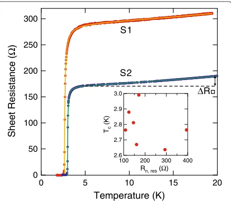
In the present study, we investigated seven samples referred to as S1, S2,... and S7. They were prepared through the identical procedure as described above, but due to subtle variations in the condition, they exhibit slightly different electron transport properties. As rep-resentative data, the temperature dependences of sheet resistanceRfor S1 and S2 are displayed in Figure 2 (red dots, S1; blue dots, S2).Rdrops to zero atTc ≈ 2.6 K
for S1 and atTc ≈ 3.0 K for S2, consistent with the
pre-vious study on the superconducting phase transition [8]. The rest of the samples show the same qualitative behav-iors. As shown below, S1 and S2 exhibit the lowest and the highest Tc, respectively, among all the samples. Here we
note two distinctive features: (i) For the high-temperature region of 5 K < T < 20 K, R decreases with decreas-ing T, i.e.,dR/dT > 0. The temperature dependence ofRis slightly nonlinear with a concave curvature, i.e.,
(a)
transport measurement unit
STM LEED
sputter gun
(c)
(b)
2 nm 20 nm
(d)
(e)
V
[image:3.595.63.539.85.488.2]1.2 mm 0.3 mm
Figure 1Instrumentation and sample preparation.The whole procedure from the sample preparation through the transport measurement was performed in a home-built UHV apparatus without breaking vacuum (a). Typical STM images of a (√7×√3)-In sample before (b) (Vsample=−0.015 V) and after (c) (Vsample=2.0 V) are displayed. (d) The design of sample patterning in the black area shows the Ar+-sputtered region. The color indicates the degree of calculated current density (green, high; purple, low). (e) Optical microscope image of a patterned sample.
The data were analyzed to deduce characteristic param-eters as follows. Feature (i) can be phenomenologically expressed by the 2D normal state conductivityG,nof the following form:
G,n=(Rn,res+CTa)−1 (1) where Rn,res is the residual resistance in the normal state, C is the prefactor, and a is the exponent of the power-law temperature dependence. Feature (ii) is natu-rally attributed to the superconducting fluctuation effects [14]. Just aboveTc, parallel conduction due to thermally
excited Cooper pairs adds to the normal electron con-duction (Aslamazov-Larkin (AL) term), and this effect
is enhanced in a 2D systems [12]. The 2D conductiv-ity due to the Cooper pair fluctuation G,sf takes the following form:
G,sf= 1
R0
T T−Tc
(2)
whereR0is a temperature-independent constant. In addi-tion to this direct effect, another indirect contribuaddi-tion may be important near Tc, which originates from the
S1
S2
R
[image:4.595.58.290.86.288.2]Δ
Figure 2Electron transport properties aboveTc.The red and blue dots represent the temperature dependences of sheet resistanceR for sample S1 and S2, respectively, while the yellow and green lines are the results of fitting analysis using Equations 1 to 3.Ris defined as the decrease inRbetween 20 and 5 K. The inset showsTc as a function ofRn,res, revealing no clear correlation between them.
pure AL term,R0 = 16/e2 = 65.8 kregardless of the thickness. Then the total sheet resistance aboveTcis given
by the following equation:
R=(G,n+G,sf)−1. (3)
The experimental data were fitted excellently using Equations 1 to 3 withRn,res,C,a,R0, andTcbeing fitting
parameters, as shown in Figure 2 (yellow line, S1; green line, S2). Since Equation 2 is only valid forT > Tc, the
data of the normal state region (defined as R > 50) were used for the fitting. All parameters thus determined are listed in Table 1 for the seven samples. We note that the obtained values for R0are all smaller by a factor of 2.4 to 5.4 than R0 = 65.8 k for the AL term. This indicates that the observed fluctuation-enhanced conduc-tivities originate from both AL and MT terms. We also tried to fit the data by explicitly including the theoretical form for the MT term [13], but this resulted in poor fitting convergence.
The determinedTcranges from 2.64 to 2.99 K. This is
in reasonable agreement with the previously determined value of Tc=2.8 K, but there are noticeable variations
among the samples. The normal residual resistanceRn,res also shows significant variations, ranging from 108 to 394. These two quantities,TcandRn,res, could be corre-lated because a strong impurity electron scattering might cause interference-driven electron localization and sup-press Tc [23]. However, they are poorly correlated, as
shown in the inset of Figure 2. This is ascribed to possible
different impurity scattering mechanisms determining
Rn,resandTcas explained in the following. Electron
scat-tering should be strong at the atomic steps because the surface layer of (√7 × √3)-In is severed there. There-fore, they contribute to most of the observed resistance [8,24]. However, the interference between scatterings at the atomic steps can be negligibly weak if the average sep-aration between the atomic stepsdavis much larger than the phase relaxation lengthLφ. This is likely to be the case becausedav ≈ 400 nm for our samples, andLφ is several tens of nanometer for typical surfaces [25]. In this case, electron localization and resultant suppression of Tcare
dominated by other weaker scattering sources within the size ofLφ, not by the atomic steps that determineRn,res.
The exponent a was determined to be 1.48 to 1.85 in accordance with feature (i). This might be seen as a typical metallic behavior due to the electron-phonon scat-tering. However, this mechanism would lead to Re-ph ∝
T for T > D and Re-ph ∝ T5 for T D [26], neither of which is consistent with the observed tempera-ture dependence. (HereRe-phis the resistance due to the electron-phonon scattering, andDis the Debye temper-ature.) Considering the exponentato be slightly smaller than 2, we attribute its origin to the electron-electron scat-tering. In a 2D Fermi liquid, it leads to a resistivityRe−e with the following form [27],
Re−e=CT2ln F
kBT
(4)
where C is a proportional constant, F is the Fermi energy, and kB is the Boltzmann constant. The log term in Equation 4 results in a weaker temperature dependence than that in a 3D Fermi liquid (∝T2). Fitting the data with Equation 4 instead of theCTa term in Equation 1 gives F≈0.1 eV, although the uncertainty is quite large.
We note that a decrease in resistance in a conventional metal film is usually very small in this temperature range. For example, it is less than 1% within the range of 2 <
T <20 K for 2-nm-thick single-crystal Nb films, although
R = 122 of the film is comparable to the observed
Rn,resin the present experiment [28]. For a metal thin film
Table 1 Summary of the fitting analysis on the resistive transition of the (√7×√3)-In surface
Sample R0(k) Rn,res() Tc(K) b R/Rn,res(%)
S1 12.1 293 2.64 1.80 8.0
S2 20.0 171 2.99 1.54 10.8
S3 15.6 146 2.81 1.78 12.6
S4 17.6 108 2.76 1.67 15.3
S5 27.7 394 2.76 1.86 5.0
S6 14.3 160 2.67 1.69 11.5
[image:4.595.305.538.619.732.2]with a large resistance,R even increases slightly with decreasing T as a consequence of the electron localiza-tion [29]. In clear contrast, a decrease inRbetween 20 and 5 K in our samples,R, amounts to as much as 5% to 15% ofRn,res (see Figure 2 and Table 1). In this sense, the observed temperature dependence is rather unusual. The (√7× √3)-In surface studied here has an atomic-scale dimension in the normal direction and may thus have an enhanced electron-electron interaction because of insufficient electrostatic screening. In comparison, the contribution from the electron-phonon interaction can be smaller because it decreases rapidly at low temperatures asRe-ph∝T5.
Residual resistance in the superconducting phase belowTc The superconducting fluctuation theories state that R
becomes exactly zero at Tc, as indicated by Equation 2.
However, a close inspection into the magnified plots (Figure 3a) reveals that R has a finite tail below Tc.
To examine whetherRbecomes zero at sufficiently low temperatures, we have taken the current-voltage (I-V) characteristics of sample S1 belowTcdown to the lowest
temperature of 1.8 K. Figure 3b displays the data in the log-log plot form. Although theI-Vcharacteristics exhibit strong nonlinearity at the high-bias current region, they show linear relations around the zero bias at all temper-atures. The sheet resistances R determined from the linear region of theI-V curves are plotted in Figure 3c as red dots.Rdecreases rapidly as temperature decreases fromTc, but it becomes saturated at approximately 2×
10−2below 2 K.
This residual resistance can be attributed to dissipation due to free vortex flow, which is caused by the Lorentz force between the magnetic flux and the current [15], since the stray magnetic field is not shielded in the experi-ment. The sheet resistance due to the free vortex flowR,v is given by the following equation:
R,v=2π ξ2R,nB/ 0 (5)
whereξis the Ginzburg-Landau coherence length,R,nis the normal sheet resistance of the sample,Bis the mag-netic field perpendicular to the suface plane, and 0 =
h/2e is the fluxoid quantum. A crude estimation using ξ = 49 nm,R,n = 290, andB = 3 ×10⁻⁵T gives
(c)
(a)
S1(b)
[image:5.595.58.543.365.676.2]S2
R,v =6.3×10⁻², which is in the same order of mag-nitude as the observed value of approximately 2×10⁻². We note thatξ = 49 nm was adopted from the value for the Si(111)-SI-Pb surface [7], andξ is likely to be smaller here considering the difference inTcfor the two surfaces.
The present picture of free vortex flow at the lowest tem-perature indicates that strong pinning centers are absent in this surface superconductor. This is in clear contrast to the 2D single-crystal Nb film [28], where the zero bias sheet resistance was undetectably small at sufficiently low temperatures. In accordance with it, the presence of strong vortex pinning was concluded from the observa-tion of vortexcreepin [28]. This can be attributed to likely variations in local thickness of the epitaxial Nb film at the lateral scale of vortex size [30]. The absence of ‘local thick-ness’ variation in the present surface system may be the origin of the observed free vortex flow phenomenon.
As mentioned above, R rapidly decreases just below
Tc. This behavior could be explained by the
Kosterlitz-Thouless (KT) transition [31,32]. In a relatively high-temperature region close to Tc, thermally excited free
vortices cause a finite resistance due to their flow motions. As temperature decreases, however, a vortex and an anti-vortex (with opposite flux directions) make a neutral bound-state pair, which does not move by current any-more. According to the theory, all vortices are paired at
TK, and resistance becomes strictly zero for an infinitely
large 2D system. The temperature dependence ofRfor
TK <T <Tcis predicted as follows:
R=Cexp
−2
b(Tc−T)
T−TK 1/2
(6)
whereCis a prefactor, andba material-dependent con-stant. For this transition to be observable, the transverse penetration depth λ⊥ for magnetic field must be larger than the sample size so that vortices can interact with each other logarithmically as a function of the mutual distance. The ultimate atomic-scale thickness of the present system leads to a very largeλ⊥in the order of millimeters [8], thus making it a candidate for observing the KT transition. We fitted the experimental data ofRusing Equation 6 within the range of 2.25 K < T < 2.61 K while Tc = 2.64 K
is fixed. The result is shown in Figure 3c as a blue line. The reasonable fitting over two orders of magnitude inR
points to the precursor of the KT transition. The obtained value ofTK =1.69 K is deviated from the relation [31]
TK/Tc≈(1+0.17R,n/Rc)−1 (7)
whereRc = /e2 = 4.11 kandR,nare identified with
Rn,res = 293of sample S1 here. However, Equation 7 is derived from the assumption of the dirty-limit BCS superconductor, which is not applicable to the (√7 × √
3)-In surface with high crystallinity. Unfortunately, the
present experimental setup does not allow us to observe the expected temperature dependence of Equation 6 down toTK because of the presence of the stray magnetic field.
Furthermore, the predicted I-V characteristics V ∝ Ia
where the exponentajumps from 1 to 3 atTK should be
examined to conclude the observation of the KT transi-tion [31,32]. Constructransi-tion of a UHV-compatible cryostat with an effective magnetic shield and a lower achievable temperature will be indispensible for such future studies.
Conclusions
We have studied the resistive phase transition of the (√7×√3)-In surface in detail for a series of samples. In the normal state, the sheet resistancesRof the samples decrease significantly between 20 and 5 K, which amounts to 5% to 15% of the residual resistivityRres. Their charac-teristic temperature dependence suggests the importance of electron-electron scattering in electron transport phe-nomena. The poor correlation between the variations in
TcandRres indicate different mechanisms for determin-ing these quantities. The decrease inRwas progressively accelerated just aboveTcdue to the superconducting
fluc-tuation effects. Quantitative analysis indicates the parallel contributions of fluctuating Cooper pairs corresponding to the AL and MT terms. A minute but finite resistance tail was found belowTcdown to the lowest temperature of
1.8 K, which may be ascribed to a dissipation due to free vortex flow. The interpretation of the data based on the KT transition was proposed, but further experiments with an improved cryostat are required for the conclusion.
Competing interests
The authors declare that they have no competing interests.
Authors’ contributions
TU and PM carried out the sample fabrication/characterization and the electron transport measurements. TU and TN conceived of the study. TU analyzed the data and drafted the manuscript. All authors read and approved the final manuscript.
Acknowledgements
This work was partly supported by World Premier International Research Center (WPI) Initiative on Materials Nanoarchitectonics, MEXT, Japan, and by the Grant-in-Aid for JSPS Fellows. The authors thank M. Aono at MANA, NIMS, for his stimulous discussions.
Received: 19 February 2013 Accepted: 21 March 2013 Published: 11 April 2013
References
1. Lifshits VG, Saranin AA, Zotov AV:Surface Phases on Silicon: Preparation, Structures, and Properties. Chichester: Wiley; 1994.
2. M ¨onch W:Semiconductor Surfaces and Interfaces. 3rd edition. Berlin: Springer; 2001.
3. Novoselov KS, Geim AK, Morozov SV, Jiang D, Zhang Y, Dubonos SV, Grigorieva IV, Firsov AA:Electric field effect in atomically thin carbon films.Science2004,306(5696):666–669.
4. Radisavljevic B, Radenovic A, Brivio J, Giacometti V, Kis A:Single-layer MoS2 transistors.Nature Nanotech2011,6(3):147–150.
6. Brun C, Hong IP, Patthey F, Sklyadneva I, Heid R, Echenique P, Bohnen K, Chulkov E, Schneider WD:Reduction of the superconducting gap of ultrathin Pb islands grown on Si(111).Phys Rev Lett2009,
102(20):207002.
7. Zhang T, Cheng P, Li WJ, Sun YJ, Wang G, Zhu XG, He K, Wang LL, Ma XC, Chen X, Wang YY, Liu Y, Lin HQ, Jia JF, Xue QK:Superconductivity in one-atomic-layer metal films grown on Si(111).Nature Phys2010,
6(2):104–108.
8. Uchihashi T, Mishra P, Aono M, Nakayama T:Macroscopic
superconducting current through a silicon surface reconstruction with indium adatoms: Si(111)-(√7×√3)-In.Phys Rev Lett2011,
107(20):207001.
9. Sakamoto K, Oda T, Kimura A, Miyamoto K, Tsujikawa M, Imai A, Ueno N, Namatame H, Taniguchi M, Eriksson PEJ, Uhrberg RIG:Abrupt rotation of the Rashba spin to the direction perpendicular to the surface.Phys Rev Lett2009,102(9):096805.
10. Yaji K, Ohtsubo Y, Hatta S, Okuyama H, Miyamoto K, Okuda T, Kimura A, Namatame H, Taniguchi M, Aruga T:Large Rashba spin splitting of a metallic surface-state band on a semiconductor surface.Nature Commun2010,1:17.
11. Bauer E, Sigrist M:Non-Centrosymmetric Superconductors. Berlin: Springer; 2012.
12. Aslamasov LG, Larkin AI:The influence of fluctuation pairing of electrons on the conductivity of normal metal.Phys Lett1968,
26A:238–239.
13. Thompson RS:Microwave, flux flow, and fluctuation resistance of dirty type-II superconductors.Phys Rev B1970,1:327–333. 14. Skocpol WJ, Tinkham M:Fluctuations near superconducting
phase-transitions.Rep Prog Phys1975,38(9):1049–1097. 15. Bardeen J, Stephen MJ:Theory of the motion of vortices in
superconductors.Phys Rev1965,140(4A):A1197–A1207. 16. Uchihashi T, Ramsperger U:Electron conduction through
quasi-one-dimensional indium wires on silicon.Appl Phys Lett2002,
80(22):4169–4171.
17. Uchihashi T, Ramsperger U, Nakayama T, Aono M:
Nanostencil-fabricated electrodes for electron transport measurements of atomically thin nanowires in ultrahigh vacuum.
Jpn J Appl Phys2008,47(3):1797–1799.
18. Kraft J, Surnev SL, Netzer FP:The structure of the indium-Si(111) (√7×√3) monolayer surface.Surf Sci1995,340(1-2):36–48.
19. Rotenberg E, Koh H, Rossnagel K, Yeom H, Sch ˜Ad’fer J, Krenzer B, Rocha M, Kevan S:Indium√7×√3on Si(111): a nearly free electron metal in two dimensions.Phys Rev Lett2003,91(24):246404.
20. Yamazaki S, Hosomura Y, Matsuda I, Hobara R, Eguchi T, Hasegawa Y, Hasegawa S:Metallic transport in a monatomic layer of in on a silicon surface.Phys Rev Lett2011,106(11):116802.
21. Park J, Kang M:Double-layer in structural model for the In/Si(111)-(√7×√3) surface.Phys Rev Lett2012,109(16):166102. 22. Uchida K, Oshiyama A:New identification of metallic phases of in
atomic layers on Si(111) surfaces.2012, arXiv:1212.1261. [http://arxiv. org/abs/1212.1261].
23. Goldman AM, Markovic N:Superconductor-insulator transitions in the two-dimensional limit.Phys Today1998,51(11):39–44.
24. Matsuda I, Ueno M, Hirahara T, Hobara R, Morikawa H, Liu CH, Hasegawa S:Electrical resistance of a monatomic step on a crystal surface.Phys Rev Lett2004,93(23):236801.
25. Jeandupeux O, Burgi L, Hirstein A, Brune H, Kern K:Thermal damping of quantum interference patterns of surface-state electrons.Phys Rev B 1999,59(24):15926–15934.
26. Ziman JM:Principles of the Theory of Solids. 2nd edition. Cambridge: Cambridge University Press; 1972.
27. Hodges C, Smith H, Wilkins J:Effect of fermi surface geometry on electron-electron scattering.Phys Rev B1971,4(2):302–311. 28. Hsu J, Kapitulnik A:Superconducting transition, fluctuation, and
vortex motion in a two-dimensional single-crystal Nb film.Phys Rev B 1992,45(9):4819–4835.
29. Bergmann G:Weak localization in thin films: a time-of-flight experiment with conduction electrons.Phys Rep1984,107:
1–58.
30. Ozer MM, Thompson JR, Weitering HH:¨ Hard superconductivity of a soft metal in the quantum regime.Nature Phys2006,2(3):173–176.
31. Epstein K, Goldman A, Kadin A:Renormalization effects near the vortex-unbinding transition of two-dimensional superconductors.
Phys Rev B1982,26(7):3950–3953.
32. Mooij JE:Two-dimensional transition in superconducting films and junction array.InPercolation, Localization, and Superconductivity. Edited by Goldman AM, Wolf SA. Berlin: Springer; 1984.
doi:10.1186/1556-276X-8-167
Cite this article as:Uchihashiet al.:Resistive phase transition of the super-conducting Si(111)-(√7×√3)-In surface.Nanoscale Research Letters2013
8:167.
Submit your manuscript to a
journal and benefi t from:
7Convenient online submission 7Rigorous peer review
7Immediate publication on acceptance 7Open access: articles freely available online 7High visibility within the fi eld
7Retaining the copyright to your article