N A N O E X P R E S S
Open Access
Structural, Optical and Electrical Properties
of Zinc Oxide Layers Produced by Pulsed
Laser Deposition Method
G. Wisz
1, I. Virt
1,2, P. Sagan
1, P. Potera
1and R. Yavorskyi
1,3*Abstract
The structural, optical, and electrical properties of zinc oxide (ZnO) layers manufactured at different process conditions were investigated. ZnO epitaxial layers were grown on silicon, glass, and ITO/glass substrates by pulsed laser deposition (PLD) technique. The influence of power beam, substrate temperature, and deposition time on films properties was analysed. Morphological features of the film surface were investigated by scanning electron microscopy. A structural study shown planar orientation of films at low temperatures of substrate, but the columnar type of growth originated in temperature enhances. Electrical properties were determined in the temperature range 300–500 K. It was shown that the type of films conductivity is metallic and it is limited by charge transfer across grain boundaries.
Keywords:Thin film, Zinc oxide, Photoconduction of ZnO, Conductive thin films, Pulse laser deposition PACS:68.35-p, 68.37.Hk, 73.50.Pz
Background
Zinc oxide is one of the most important group II–VI
semiconductor materials. It is a wide-bandgap oxide semiconductor with a direct energy gap of about 3.37 eV. ZnO has high chemical and mechanical stability; furthermore, it is nontoxic and widespread in nature. Recently, transparent-conducting oxides on the base of ZnO have been studied well [1–3]. ZnO is one of the most promising materials for the fabrication of the next gener-ation of optoelectronic devices in the UV region and optical or display devices [4]. As a matter of fact, simul-taneous occurrence of both high optical transmittances in the visible range and low resistivity make ZnO an import-ant material for manufacturing of heat mirrors used in gas stoves, conducting coatings in aircraft glasses to avoid surface icing, and thin film electrodes in amorphous silicon solar cells. ZnO belongs to hexagonal wurtzite class; it is a semiconducting, piezoelectric, and optical waveguide material used in sensors, surface acoustic
devices, transparent electrodes, and solar cells [5–7]. Controlling of ZnO physical properties depending on various factors, such as doping and temperature growth, is important for efficient function of devices on the base of ZnO structures. The existence of both (nandp) conduc-tion types is of fundamental importance for applicaconduc-tion in light-emitting devices [8]. The nanostructures like nano-tubes, nanorods, nanowalls, nanofibers and high-quality undoped and doped ZnO thin films have been grown with plasma-assisted molecular beam epitaxy, vapor transport deposition method, vacuum arc deposition metal organic
chemical vapor deposition (MOCVD), sol–gel process,
and spray pyrolysis [9, 10]. Such nanotubes, nanowires, nanoribbons, and nanofibers have deserved special atten-tion for their potential applicaatten-tions in applied fields such as field emission displays, optical waveguides, solar cells, ultraviolet photodetectors, optical switches, and gas sensing [1–8]. The chemical bath deposition and sol–gel technique are also well known methods of preparation of ZnO thin films. Among these methods, spray pyrolysis is useful in wide range of applications [11, 12]. This method is cheaper, simpler and permits to obtain films for opto-electronic applications with required properties. Structural, electrical, and optical properties dependence on thickness
* Correspondence:[email protected]
1Rzeszow University, Rejtana 16C, 35-959 Rzeszow, Poland
3Vasyl Stefanyk PreCarpathian National University, T. Shevchenko, 57, 76018 Ivano-Frankivsk, Ukraine
Full list of author information is available at the end of the article
of ZnO films has been investigated. The unique and fascin-ating properties of nanostructured materials have triggered tremendous motivation among scientists to explore the possibilities of using them in technological applications. In particular, the electronic and optical properties of nano-structure materials have been of great interest because of their potential applications in the fabrication of microelec-tronic and optoelecmicroelec-tronic devices [13].
In this paper, the electrical, structural, and optical properties of ZnO nanostructured thin film deposited by PLD method and their changes during annealing have been investigated.
Methods
The ZnO films grown on silicon, glass, and ITO/glass
were deposited by the PLD method. The YAG: Nd3+
laser with the 532 nm (II harmonics) wavelength, 6 ns
pulse time, and 16 J/cm2 fluence was used. The laser
beam was focused on the target using a quartz lens with focal distance of 600 mm. The pressed ZnO powder was used as a target. The growth temperatureTswas kept in
the range 20–400 °C and the deposition of the layers
was carried out at 10−8mbar vacuum.
Structural properties and cross-sectional images of the film were investigated by scanning electron microscopy Vega3 Tescan, for samples growth at the temperatureTs=
200 and 300 °C. The electrical characterization was carried out in a four probe conductivity cells. A constant voltage was applied to the sample and the current was measured using a Keithley electrometer. Current dependences on temperature were recorded during the cooling as well. When the samples reached the room temperature, it was taken to second heating–cooling cycle. During the second
heating–cooling cycle, also the current dependence on
temperature was recorded. The cycle curves were mea-sured for films as grown and after annealing in oxygen atmosphere in 250 °C. Optical transmission spectra were
measured in the wavelength range of 190–1100 nm using
UNICAM UV300 spectrometer. The photoconductivity of
thin films ZnO was determined by measuring resistance/ conductivity of the films using the illumination by light-emitted diode with 365 nm.
Results
Structural Properties
Surface morphology and cross section of ZnO samples deposited at growth temperatureTs= 200 and 300 °C are
presented in Figs. 1 and 2, respectively. There is spher-ical precipitate with 680 nm size on the thin films surface which shows the uniform structure. At higher growth temperature, the structure of ZnO films is more uniform (Fig. 1b) and the size of spherical precipitate at
Ts= 300 °C is less than atTs= 200 °C.
Formation of the layer structure is observed at Ts=
200 °C on the cross section of ZnO thin film (Fig. 2a). At higher substrate temperatureTs= 300 °C, the
colum-nar type of growth is observed for ZnO films (Fig. 2b). Columnar growth of the thin films indicates that ZnO films havec-axis preferred orientation.
Electrical Characterization
The photoresponse of ZnO consists of two parts: a rapid process of photogeneration and recombination of electron-hole pairs and a slow process attributed to the oxygen adsorption and photodesorption on the film surface as well as the grain boundaries.
Columnar growth with temperature increasing is accompanied by increase of the layer resistance value which was observed on the plotsR(T) for sample at the
Ts= 300 °C (Fig. 3a). Increase of average distance
be-tween the crystal columns affects increasing potential barrier at the grain boundaries and thus increasing resistance of the layer in the plane of the substrate. For the layer planar structure at Ts= 200 °C, increasing of
resistance is not so clearly observed.
For the sample obtained atTs= 300 °C after annealing
(Fig. 3b), the clear and sharp increase of cross-resistance layer with the increase of temperature is observed. This
[image:2.595.59.540.574.714.2]behavior can be caused by a large number of clear boundaries between the crystalline ZnO columns. On
the other hand, for a sample obtained at Ts= 200 °C
(Fig. 3b), the decrease of resistance with increasing temperature which may indicate the different orientation of crystallite is obtained.
The resistivity value of 0.95 × 10⁻¹ Ωcm
(polycrystal-line thin films obtained at Ts= 300 °C), is about one
order higher than the resistivity of films obtained by other methods, including high-frequency sputtering oxide target. Semiconductor behavior has films grown only at low temperatures. The presence of metal con-ductivity in films and blue shift of the optical bandgap indicate the presence of relatively high carrier concentra-tion. This can be caused by annealing and the effective concomitant decrease of the oxygen defects in ZnO. As-grown and annealed films show different scattering mechanisms. There are some types of oxygen defects in these films, such as oxygen defects, oxygen vacancies (VO), and interstitial oxygen atoms (Oi). Annealing in
oxygen atmosphere allows the reduction of a number of point defects. Metal conductivity determines the behav-ior of carrier scattering in severely defective degenerate semiconductors, while the semiconductor character de-fines the activation processes. In general, the degenerate
of electronic conduction in ZnO thin films is a combination of both processes: scattering of carriers and their activation. Thus, structural properties of thin films of ZnO can be determined from the temperature dependence of electrical resistance as shown in Fig. 3. In this case, the value of the carrier
concentration n0 is supposed to be dependent weakly
on temperature and it caused by intrinsic defects such as oxygen vacancies and interstitial zinc. In these films, the mobility depends initially on the temperature, in-creases to a maximum, and then dein-creases with increasing temperature [14].
In the presence of various scattering mechanisms that control the mobility of electrons in ZnO polycrystalline thin films, mostly limited mobilities are scattering grain (grain)μg, scattering latticeμl, and (at low temperatures)
ionized impurity scattering μii. Thus, the total mobility
is given by
1
μ¼
1
μl þμ1
g þμ1
ii
ð1Þ
At higher temperatures, which are used in these studies, a significant contribution to the mobility makes the lattice
Fig. 2The cross-sectional images of ZnO films deposited at the different substrate temperaturesTs:a200 °C;b300 °C
1 2 3
2,0 2,2 2,4 2,6 2,8 3,0 3,2 3,4 3,6 104
105
106
m
h
O
,
R
103
/T, K-1
2,0 2,2 2,4 2,6 2,8 3,0 3,2 3,4 3,6 103
104
105
106
m
h
O
,
R
103/T,K-1
1 2 3
[image:3.595.57.541.89.228.2] [image:3.595.61.539.580.712.2]scattering, as can be expected. It is determined by the expression:
μ1 ¼
π
3 1=3
⋅ eh3Cl
m
ð Þ2
Ed2kBTB ⋅ 1
n1=3 ð2Þ
Here,his Planck’s constant,kis Boltzmann’s constant,
m* is the effective mass of electron, T is absolute
temperature, Ed is deformation potential constant,Cl is
the elasticity modulus of system, andnis the concentra-tion of electrons. Thus, the equaconcentra-tion can be written in a short form μ1¼B
T⋅
1
n1=3 (B is some constant) that deter-mines the mobility grid proportional to the reciprocal temperature. The experimental curves show linear fit conductivity of T−1, and it confirms the superiority of lattice scattering in the range of high temperatures of 300 to 400 K. In addition, the slope changing of straight line is consistent with polycrystalline films grown at higher temperatures. Another scattering temperature mechanism mode operates at room temperature (300 K), which limits the electron mobility due to grain boundar-ies scattering (GBS). It is assumed that this is due to the column growth form at high substrate temperatures and increasing role of grain boundaries in the film annealing in an oxygen atmosphere.
The correlation between the structural characteristics, properties, and photovoltaic electric transport properties of films were evaluated by measuring of photoresponse of films, especially under UV irradiation.
The photoconductivity response was performed with the illuminated light of 365 nm. The curves of photocon-ductivity response of a ZnO films grown at temperature
Ts= 20–400 °C is shown in Fig. 4a. The photocurrent for
thin films withTs= 300 °C rises within 3 min and falls to
50% of its maximum value within 6 min.
A very pronounced photoconductivity effect is
observed in Fig. 4b for samplesTs= 300 and 400 °C after
the annealing. There is an extremely rapid excitation and fast relaxation occurring during the 280 s for the sampleTs= 400 °C.
Optical Properties
Optical characterization of thin films gives information about other physical properties, e.g., bandgap energy, band structure, and optically active defects. The effects of thickness and annealing on the optical transmittance and the bandgap (Eg) values of the ZnO films have been
studied. The optical transmission (T, %) of the ZnO films
formed at the growth temperature Ts= 20–300 °C is
shown in Fig. 5a and after anneals in Fig. 5b. The
a
b
Fig. 4Photoconduction of the samples (1PLD,2PLD-200A,3PLD-300, and4PLD-400) thin film ZnO as-growth (a) and annealed (b)
200 400 600 800 1000 0
20 40 60 80 100
a
n
oi
s
si
m
s
n
ar
T
%
Wavelength (nm)
1 2 3 4
200 400 600 800 1000 0
20 40 60 80 100
b
n
oi
s
si
m
s
n
ar
T
%
Wavelenght(nm)
1 2 3 4
[image:4.595.61.539.88.226.2] [image:4.595.61.540.579.713.2]transmission decreases sharply in the near ultraviolet re-gion due to the bandgap absorption. Absorption edge takes place around 350 nm for all samples. Note that these films exhibit transparency in the visible range of the average transmittance, which lies between 30 and 70%. In addition, the lack of interference fringes in the transmission spectra is due to surface roughness, tower height, and scattering at the grain boundaries. Also, there is the skip increases at low-temperature annealing of films. Increased optical transmission associates with a decrease in oxygen defects. In parallel, the absorption tails can be observed in the visible region, which is characteristic for disordered systems (e.g., glassy) [15].
The samples have an average optical transparency of
60–70% in the region from 800 to 1100 nm and a sharp
edge adsorption after annealing (Fig. 5b), which for all samples is approximately 360 nm. In order to obtain the bandgap, the absorption coefficient was calculated from the transmission data using the following relation:
α¼ ln 1ð =T rÞ
d ð3Þ
where d is the film thickness and Tr is the
transmit-tance. On the other hand, beyond the band edge, the absorbance is very small and the transmittance is high. This indicates a low amount of impurities and a few lat-tice defects in obtained films. Also, the flat range of the transmission curves without interference fringes empha-sizes the surface uniformity with small crystallite size. Here, the fabricated ZnO films are considered as a material having direct bandgap energy [16]. For the direct transition, the optical bandgap energy of ZnO film was determined using the equation:
αhν
ð Þ2¼
A hν−Eg
ð4Þ
whereAis a constant, andhνis the photon energy, and
Egis the optical energy gap.
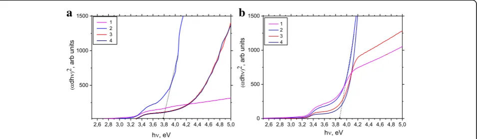
Figure 6 shows a graph (αhν)2 versus photon energy, allowing assessing the value of the energy gap with a sharp edge absorption using linear approximation.
Estimated values of optical energy gap Eg of ZnO thin
films are shown in Table 1. The results show an increase in the optical energy gap with increase of deposition temperature. This increase in the energy gap can be according to the considerable shift Burstein electron density [17]. Presence of tail absorption profile in the
visible range gives Urbach energy Eu, induced optical
absorption on own defects. It can be estimated from the empirical Urbach law [18],
αð Þ ¼hν α0e hv EU
EU¼αð Þhν
d½αð Þhν d h½ ν
−1
¼h d
dvðlnαð ÞhνÞ
−1
8 > > > < > > > :
;
ð5Þ
where α represents the experimentally determined
optical absorption profile and α0is constant. Eu
param-eter is defined as the reciprocal value of the recession spectral characteristics for different films presented in Table 1. That formation of tail states zone in the for-bidden zone indicates the spin-exchange interaction between the conduction electrons and electrons local-ized at defects and their interaction with phonons.
a
b
[image:5.595.305.539.110.180.2]Fig. 6Optical energy gap of the samples (1PLD,2PLD-200A,3PLD-300, and4PLD-400) thin films ZnO as-growth (a) and annealed (b)
Table 1The variation of bandgap energy and Urbach’s energy of ZnO thin films
Sample Ts, °C Eg, eV Eu, eV Sample (anneal) Eg, eV Eu, eV
PLD 20 3.30 0.14 PLD an 3.58 0.27
PLD-200 200 3.79 0.36 PLD-200 an 3.87 0.32
PLD-300 300 4.08 0.18 PLD-300 an 3.83 0.12
[image:5.595.61.539.575.714.2]Discussion
As described above, the surface conduction mechanism is mainly related to the absorption or desorption of chemisorbed oxygen. In the dark state, chemisorbed oxygen molecules capture free electrons: O2(g) +e−→
O2−. This process leads to the formation of the depleted
surface layer and causes the bending energy as areas of conduction and valence band. Formation of large amounts of ionized oxygen on the surface of ZnO in-creases the bending zones, leading to the formation of a potential barrier, and therefore to increased resistance. In terms of lighting UV light photos generated and adsorbed (O2) particles released: O2(g) +hν→O2−+e−.
O2neutral molecules embedded in the grain boundaries
form oxygen ions and free electrons in the processes as-sociated with polycrystalline. In this case, released by the light, the generated electrons contribute to the photo-conductivity. The processes related to the intergrain boundaries are responsible for the faster process than the surface processes because of the large number of structural defects and defects in grains. In particular, the ZnO film, which is characterized by very small grains, can save a significant amount of adsorbed oxygen at the grain boundaries, which leads to higher number of car-riers. In contrast, samples obtained at higher tempera-tures have the biggest grains; therefore, the number of carriers is decreased with trap number as expected with a fast response time. Thus, the current recession should be described by two mechanisms. The first one is related to the process of electron-hole recombination by chemi-sorbed oxygen atoms and a damping mechanism that is essentially independent of grain size and also depends on the temperature. The second one decay occurs through a process of recombination of electron-hole pairs by chemisorbed oxygen and defects on the surface. This process is generally much slower than the previous one. The decay time increases with temperature of ZnO deposition. This can be explained by taking into account the amount of chemisorbed oxygen on the surface at a higher temperature deposition. Thus, the grain size and the amount of adsorbed oxygen are probably the main parameters, which mainly manage the properties of photoresponse decay.
Conclusions
ZnO thin films have been successfully deposited using pulsed laser deposition technique at different substrate
temperatures that vary in the range of 20–400 °C. The
experimental curves show a linear dependence of the electrical conductivity versus reciprocal temperature, and this confirms the superiority scattering lattice. This is the columnar film growth at higher substrate tempera-tures. At room temperature, electron mobility is limited by scattering grain boundaries. Photoconductivity curves
are characterized by two distinct trends in photocurrent decay with a time constant that depends on the mechan-ism of recombination of nonequilibrium carriers.
Abbreviations
ITO:Indium tin oxide; MOCVD: Metal organic chemical vapor deposition; PLD: Pulsed laser deposition
Acknowledgements
This work was performed under the Science Department Laboratory of Material Technologies for Industry, University of Rzeszow.
Funding
All sources of funding for the research were based from statutory activities of the University of Rzeszow.
Authors’Contributions
GW grown thin films, has performed and determined the problem, and has defined the methods and subjects of the investigation as well as made a SEM cross-sectional images. PP has conducted the research on the optical properties of thin films. PS has obtained the SEM images. IV has conducted the research on thin films of the electrical parameters and took a part in the discussion of the experimental results. RY conducted the experiments, performed the characterization, interpreted the results, and wrote the manuscript. All authors have read and approved the final version of the manuscript.
Authors’Information
GW is a doctor of physical sciences, President of the Management of
Subcarpathian Renewable Energy Cluster, University of Rzeszow, Rzeszow, Poland. PS is a doctor of physical sciences Laboratory Research and Environmental Monitoring, University of Rzeszow, Rzeszow, Poland.
PP is a doctor of physical sciences Laboratory of Material Technologies for Industry, University of Rzeszow, Rzeszow, Poland. IV is a professor of physical sciences Laboratory Research and Environmental Monitoring, University of Rzeszow, Rzeszow, Poland, and a professor of Engineering and Technology Fundamentals Department, Drohobych State University, Drohobych, Ukraine. RY is a master of physical sciences, University of Rzeszow, Rzeszow, Poland, and a PhD student at the Physics and Chemistry of Solid State Department, Vasyl Stefanyk PreCarpathian National University, Ivano-Frankivsk, Ukraine.
Completing Interests
The authors declare that they have no competing interests.
Publisher’s Note
Springer Nature remains neutral with regard to jurisdictional claims in published maps and institutional affiliations.
Author details
1Rzeszow University, Rejtana 16C, 35-959 Rzeszow, Poland.2Drohobych State University, I. Franko, 24, 82100 Drohobych, Ukraine.3Vasyl Stefanyk PreCarpathian National University, T. Shevchenko, 57, 76018 Ivano-Frankivsk, Ukraine.
Received: 30 December 2016 Accepted: 30 March 2017
Reference
1. Zhang Q, Zhao Y, Jia Z, Qin Z, Chu L, Yang J, Zhang J, Huang W, Li X (2016) High stable, transparent and conductive ZnO/Ag/ZnO nanofilm electrodes on rigid/flexible substrates. Energies. doi:10.3390/en9060443
2. Liu Y, Li Y, Zeng H (2013) ZnO-based transparent conductive thin films: doping, performance, and processing. Journal of Nanomaterials. doi:10.1155/2013/196521
3. Ahn S, Jeon Y, Ahn J-H, Song I, Jeon S, Yun D-J, Kim J, Hyung Choi H, Chung U-I, Park J (2013) Impact of transparent electrode on photoresponse of ZnO-based phototransistor. Appl Phys Lett. doi:10.1063/1.4855055 4. Huang H, Fang G, Mo X, Long H, Yuan L, Dong B, Meng X, Zhao X (2009)
5. Zheng ZQ, Yao JD, Wang B, Yang GW (2015) Light-controlling, flexible and transparent ethanol gas sensor based on ZnO nanoparticles for wearable devices. Sci Rep. doi:10.1038/srep11070
6. Shih CC, Lee WY, Chiu YC, Hsu HW, Chang HC, Liu CL, Chen WC (2016) Transistor memory devices using nano-floating gate of polymer/ZnO nanocomposites. Sci Rep. doi:10.1038/srep20129
7. Umit O, Daniel H, Hadis M (2010)ZnOdevices and applications: a review of current status and future prospects. Proc IEEE. doi:10.1109/JPROC.2010.2044550 8. Ozgür U, Alivov YI, Liu C, Teke A, Reshchikov MA, Doğan S, Avrutin V, Cho
SJ, Morkoç HA (2005) comprehensive review of ZnO materials and devices. J Appl Phys. doi:10.1063/1.1992666
9. Li X, Shen R, Zhang B, Dong X, Chen B, Zhong H, Cheng L, Sun J, Du G (2011) Nitrogen doped ZnO thin films prepared by photo-assisted metal-organic chemical vapor deposition. J Nanosci Nanotechnol.
doi:10.1166/jnn.2011.5329
10. Roshchina NM, Smertenko PS, Stepanov VG, Zavyalova LV, Lytvyn OS (2013) Some properties of thin film structures on the base of ZnO obtained by MOCVD method. Solid State Phenomena. doi:10.4028/www.scientific.net/ SSP.200.3
11. Shaikh SK, Inamdar SI, Ganbavle VV, Rajpure KY (2016) Chemical bath deposited ZnO thin film based UV photoconductive detector. J Alloys Compd. doi:10.1016/j.jallcom.2015.12.226
12. Ayana DG, Prusakova V, Collini C, Nardi MV, Tatti R, Bortolotti M, Lorenzelli L, Chiappini A, Chiasera A, Ferrari M, Lunelli L, Dirè S (2016) Sol–gel synthesis and characterization of undoped and Al-doped ZnO thin films for memristive application. AIP Advances. doi:10.1063/1.4968192
13. Dutta S, Chattopadhyay S, Sarkar A, Chakrabarti M, Sanyal D, Jana D (2009) Role of defects in tailoring structural, electrical and optical properties of ZnO. Progress in Materials Science. doi:10.1016/j.actamat.2016.03.012 14. Singh A, Chaudhary S, Pandya DK (2016) High conductivity indium doped
ZnO films by metal target reactive co-sputtering. Acta Mater. doi:10.1016/j. actamat.2016.03.012
15. Mimouni R, Kamoun O, Yumak A, Mhamdi A, Boubaker K, Petkova P, Amlouk M. Effect of Mn content on structural, optical, opto-thermal and electrical properties of ZnO: Mn sprayed thin films compounds// Journal of Alloys and Compounds 2015 doi:10.1016/j.jallcom.2015.05.012
16. Zhang D, He Y, Wang CZ (2010) Structure and optical properties of nanostructure zinc oxide films with different growth temperatures. Optics & Laser Technology. doi:10.1016/j.optlastec.2009.10.003
17. Caglar M, Ilican S, Caglar Y, Yakuphanoglu F (2008) Electrical conductivity and optical properties of ZnO nanostructured thin film. Appl Surf Sci. doi:10.1016/j.apsusc.2008.11.055
18. Shim ES, Kang HS, Pang SS, Kang JS, Yun I, Lee SY (2003) Annealing effect on the structural and optical properties of ZnO thin film on InP. Materials Science and Engineering. doi:10.1016/S0921-5107(02)00622-0
Submit your manuscript to a
journal and benefi t from:
7 Convenient online submission
7 Rigorous peer review
7 Immediate publication on acceptance
7 Open access: articles freely available online
7 High visibility within the fi eld
7 Retaining the copyright to your article