BUCK CONVERTER SWITCHING DESIGN USING MICROCONTROLLER
IZWAN BIN CHE SHAM
A project report submitted in partial
fulfillment of the requirement for the award of the
Degree of Master of Electrical Engineering
Faculty of Eectrical and Electronics Engineering
Universiti Tun Hussein Onn Malaysia
v ABSTRACT
vi ABSTRAK
vii CONTENTS
TITLE i
DECLARATION ii
DEDICATION iii
ACKNOWLEDGEMENT iv
ABSTRACT v
ABSTRAK vi
CONTENTS vii
LIST OF TABLE ix
LIST OF FIGURES x
LIST OF SYMBOLS AND ABBREVIATIONS xiii
CHAPTER1 INTRODUCTION 1 1
1.1 Research background 1
1.2 Problems Statement 3
1.2.1 Research Objective 3
CHAPTER 2 LITERATURE REVIEW 4
2.1 DC to DC conversion method 4
2.2 Buck converter 7
2.3 Buck converter operation 7
2.4 Buck converter duty cycle 9
2.5 CCM and DCM 10
viii
CHAPTER 3 METHODOLOGY 17
3.1 Components selection 17
3.1.1 DC voltage source 18
3.1.2 Inductor 18
3.1.3 Capacitor 18
3.1.4 Diode 19
3.1.5 MOSFET 19
3.1.6 IR2101 20
3.1.7 PIC18F4550 microcontroller 20
3.2 Software selection 21
3.2.1 MPLAB IDE 21
3.2.2 Proteus 22
3.3 PWM Programming 23
3.3.1 Capture/Compare/PWM (CCP) modules 23
3.3.2 PWM period 25
3.3.3 PWM duty cycle 25
3.3.4 Setup for PWM operation 26
3.4 Circuit construction 26
CHAPTER 4 SIMULATION AND RESULT 31
4.1 Parameter setting 31
4.2 Simulation result 32
4.3 Simulation analysis 36
CHAPTER 5 CONCLUSION 38
ix
LIST OF TABLE
Table 1: Key parameter for buck converter simulation 31
x
LIST OF FIGURES
1 Voltage divider 5
2 Linear voltage regulator 6
3 DC-DC converter 6
4 Buck converter 7
5 Switch Q closed 8
6 Switch Q open 9
7 Duty cycle 9
8 (a) CCM (b) DCM 10
9 Buck converter operation (a) Q turn on (b) Q turn off 11
xi 11 PIC18 family
21
12 PIC18F4550 21
13 MPLAB window 22
14 Proteus window 23
15 CCP module in PWM mode 24
16 PWM output 25
17 The complete buck converter circuit 27
18 PWM programming 27
19 PWM programming compilation 29
20 Loading the hex file 29
xii 22 Output voltage
32
23 Output current 32
24 Input current 33
25 PWM output with 0.95 duty cycle 33
26 Inductor current 34
27 Diode voltage drop 34
28 Diode current 35
xiii
LIST OF SYMBOLS AND ABBREVIATIONS
DC - Direct current
PWM - Pulse Width Modulation
V - Voltage
A - Ampere
m - mili
CCM - Continuous Conduction Mode DCM - Discontinuous Conduction Mode KVL - Kirchhoff's Voltage Law
MOSFET - Metal Oxide Semiconductor Field Effect Transistor IGBT - Insulated Gate Bipolar Transistor
PIC - Peripheral Interface Controller
Hz - Hertz
I/O - Input/Output
CCP - Capture/Compare/PWM USB - Universal Serial Bus
ADC - Analog-to-Digital (A/D) converter SPI - Serial Peripheral Interface
1 CHAPTER 1
INTRODUCTION
This chapter will review on the basic of a buck converter and its applications.
1.1 Research background
Step-down switching or buck converters are vital to modern electronics. They can convert a voltage source (typically 8 V to 25 V) into a lower regulated voltage
(typically 0.5 V to 5 V). Step down converters transfer small packets of energy using a switch, a diode, an inductor and several capacitors. Though considerably larger and noisier than their linear-regulator counterparts, buck converters offer higher efficiency in most cases.
As usually known, the conventional buck converter [5] [6] is widely used in the industry. DC–DC converters have been effectively controlled for many years using analog integrated circuit technology and linear system design techniques [4].
2
the electronic power switches, shown reduced noise immunity and difficulty to assure further developments or new more complex control functions.
Digital control in power electronics has been intensively used during the last decade [1]. The improved performances and price reduction of digital controller has enable their application in power electronic control.
The primary advantages of digital control over analog control are higher increased flexibility by changing the software, more advanced control techniques and reduced number of components [2]. The implementation of complex control
function with analog circuits is difficult but using a digital programmable device the implementation becomes easier [3]. Digital controllers offer several benefits as summarized below [9]:
Provision of new capabilities such as implementation of advanced algorithms enabling higher performance, and lower energy consumption, among other things.
Immunity to drifts since digital controller’s functioning is substantially unaffected by either time or temperature drifts. Equations in software do not drift, unlike analog controllers.
Software implemented on programmable controllers can calibrate out the inaccuracies and can automate this calibration process, hence lowering the cost of manufacturing by eliminating a manual calibration step.
Ease of implementation since functions are easily implemented in software. Faster time to market since digital controllers make it possible to leverage
existing off-the-shelf controllers, which allow the fastest realization of a design. In addition, the design of controllers is often an iterative process, with repeated design and test steps, until the specifications are met. Such an iterative process can be executed rapidly by means of a software-configurable controller.
Control law changes are done by software updates, hence a much faster process than incorporating these changes with hardware.
3
A significant difficulty in power electronics is to control or to design main controllers for different kind of switched mode converters. The regulation is normally achieved by the pulse width modulation (PWM) at a fixed frequency [1]. The efficiency characteristics of a buck converter, however, change dramatically as the switching frequency is increased [10]. The switching device is a power MOSFET [7].
1.2 Problems Statement
Analog control technology has been successfully employed in controlling the operation of DC-DC converter. But analog technology has many disadvantages that limit the buck converter operation. Digital technology has been considered to replace the analog technology. This project will investigate the ability of digital control of the buck converter using microcontroller to control the operation of the DC-DC converter.
1.2.1 Research Objective
To implement digital technology using microcontroller for controlling buck converter operation.
4 CHAPTER 2
LITERATURE REVIEW
This chapter will cover topic on buck converter issues.
2.1 DC to DC conversion method
There are three techniques to convert DC voltage from higher value to lower value. These techniques are:
Voltage divider
Linear voltage regulator DC-DC converter (buck)
5
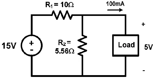
Figure 1: Voltage divider
Kirchhoff's voltage law (KVL) tell that there should be 15V – 5V = 10V across the 10Ω resistor and, therefore, we are drawing 1A from the 15V supply. Thus the voltage divider efficiency, η is:
% 33 . 3 100 15 5 . 0 100 ) 1 ( 15 ) 100 ( 5
100
W W A V mA V P P IN OUT
Clearly the voltage divider is not effectively using input voltage energy. In fact the circuit is wasting (1A) 2 10Ω =10W in the one resistor and (5V) 2 / 5.56Ω = 4.5W in the other.
Figure 2 shows linear voltage regulator using LM317 chip. The LM317 works by creating 1.25V across the 120 Ω resistor. So the current in 120 Ω resistor, I120 Ω = 1.25V /120 Ω =10.4mA. With zero current leaving the bottom of the chip, this means that there is 10.4mA x 360 Ω = 3.75V across the bottom resistor, so that there is always 1.25V + 3.75V = 5V across the load.
Using KCL, output current from LM317, I317(out) = 100 mA + 10.4 mA. Then applying KCL to the entire LM317 chip, the input current must be the same as the output current or I317(in) = I317(out) = 110.4 mA. We can then calculate the efficiency as
% 2 . 30 100 656 . 1 5 . 0 100 ) 4 . 110 ( 15 ) 100 ( 5
100
6
Figure 2: Linear voltage regulator
Even though the efficiency is better than voltage divider, linear voltage regulator are still inefficiently using the power supply energy and wasting 1.656W - 0.5W = 1.156W in the chip and resistors.
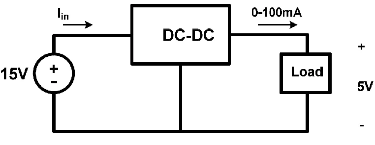
Figure 3: DC-DC converter
With a buck converter with assuming efficiency of 92%, the required input power from the supply is
W W
P P OUT
in 0.543
92 .
5 . 0
[image:16.612.119.500.410.558.2]7
Thus we are only “wasting” 0.543W - 0.5W = 0.043W and the required input current has dropped to Iin = Pin / Vin = 0.543W /15V = 36.2 mA. The converter is drawing far less current from the supply voltage with improved efficiency.
2.2 Buck converter
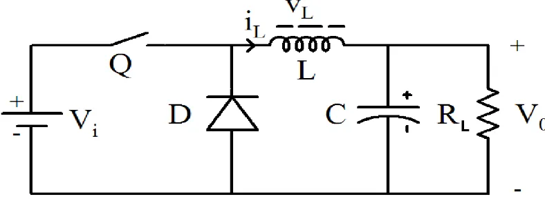
A buck converter is a step-down DC to DC converter. For a DC–DC converter, input and output voltages are both DC. It uses a power semiconductor device as a switch to turn on and off the DC supply to the load.
[image:17.612.162.556.388.532.2]The switching action can be implemented by a BJT, a MOSFET, or an IGBT. Figure 4 shows a simplified block diagram of a buck converter that accepts a DC input and uses pulse-width modulation (PWM) of switching frequency to control the switch. An external diode, together with external inductor and output capacitor, produces the regulated dc output. Buck, or step down converters produce an average output voltage lower than the input source voltage.
Figure 4: Buck converter
2.3 Buck converter operation
8
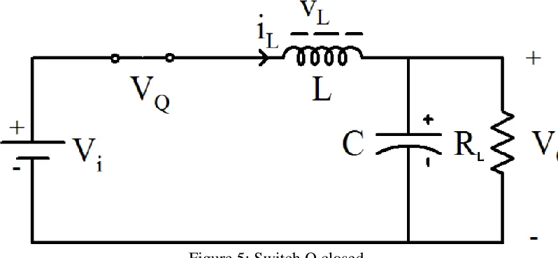
[image:18.612.130.529.264.449.2]When switch Q closes, current flows from the supply voltage Vi through the inductor and into the load, charging the inductor by increasing its magnetic field and increasing Vo. Diode D will be on reverse bias, thus blocking the path for current. An inductor reduces ripple in current passing through it and the output voltage would contain less ripple content since the current through the load resistor is the same as that of the inductor. At the same time, the current through the inductor increases and the energy stored in the inductor increases. When Vo reaches the desired value, switch Q is open and diode D is turned on. Figure 5 shows this mode.
Figure 5: Switch Q closed
9
Figure 6: Switch Q open
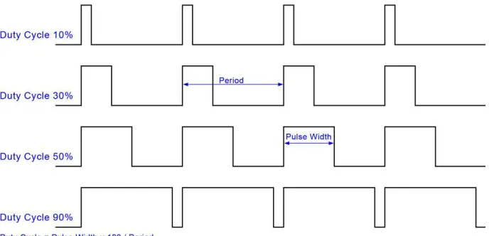
2.4 Buck converter duty cycle
The ratio of output voltage, Vout to input voltage, Vin can be adjusted by varying the duty cycle of switch Q. The longer Q is turned on, the greater Vout will be. The duty cycle of Q is usually called the converter’s duty cycle. If the switches and the inductor are lossless, Vin is converted to Vout with no loss of power and the conversion is 100% efficient. Figure 7 shows variation of duty cycle.
Duty cycle is always being presented in percentage value. A 60% duty cycle means the power is on 60% of the time and off 40% of the time. While a 50% duty cycle means the power is on 50% of the time and off 50% of the time.
[image:19.612.160.504.523.689.2]
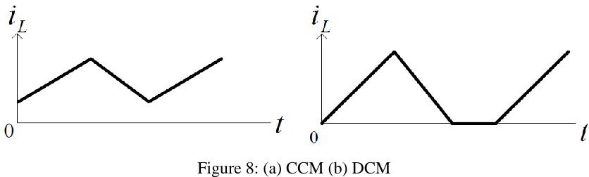
10 2.5 CCM and DCM
The buck converter can operate in two different modes; continuous conduction mode (CCM) and discontinuous conduction mode (DCM). The difference between the two is that in CCM the current in the inductor does not fall to zero.
A buck converter operates in continuous mode if the current through the inductor never falls to zero during the commutation cycle. In DCM, the current through the inductor falls to zero during part of the period. Practically, converter can operated in either operation modes. Figure 8 shows CCM and DCM mode.
Figure 8: (a) CCM (b) DCM
2.6 Buck converter analysis
The initial study of this circuit utilizes the following assumptions. Capacitor is large enough that the output voltage ripple is small relative to its average value. Inductor is large enough to ensure that the inductor current stays positive for the switching period. This is referred to as continuous conduction mode or CCM.
This ensures that when the switch is off, the diode must be on. All components are initially assumed ideal. The circuit is in the steady state, implying that all waveforms are in fact periodic, ensuring that they have the same value at the beginning and end of a switching period.
[image:20.612.119.537.259.385.2]11
Figure 9: Buck converter operation (a) Q turn on (b) Q turn off
By using Kirchhoff's Voltage Law (KVL), the voltage across the inductor when switch Q is closed is:
o Q i
L V V V
V (2.0)
At the same time, the voltage VL across the inductor is related to the change in current flowing through it which is:
dt di L
12 Rearranging equation (2.0) will result in:
o Q i L
V V V dt di
L
So the amount of inductor current is:
L V V V
dt
diL i Q o
(2.2)
The duty cycle of the buck converter is defined as:
T T T
T T
D ON
OFF ON
ON
(2.3)
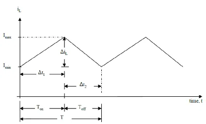
[image:22.612.115.540.434.689.2]From Figure 10, dt = ∆t1 = TON
13
So the inductor current increase during the on state is given by:
ON o Q i L T L V V V on
I
( ) (2.4)
When switch Q open, the voltage across inductor is:
D o
L V V
V (2.5)
D o L V V dt di
L
L V V dt
diL o D
(2.6)
Again from Figure 7, dt = ∆t2 = TOFF
So the inductor current increase during the on state is given by:
OFF D O L T L V V off
I
( ) (2.7)
For steady-state operation, ΔIL (on) and ΔIL (off) must be equal. Or else, the inductor current would have a net increase or decrease from cycle to cycle which would not be a steady state condition. Thus, these two equations can be equated and solved for VO to obtain the continuous conduction mode buck voltage conversion relationship.
) ( )
(on I off
IL L
(2.8)
ON o Q i T L V V V
= O D OFF
T L
14 OFF D OFF o ON o ON Q ON
iT V T VT VT V T
V
OFF D ON Q ON i OFF O ON
OT V T VT V T V T
V
OFF D ON Q ON i OFF ON
O T T VT V T V T
V ( )
OFF D Q i ON
OT T V V V T
V ( )
T T V V V T
VO ON i Q D OFF
( ) T T V D V V V OFF D Q i
O ( ) (2.9)
And using
T T D OFF
1 (2.10) ) 1 ( )
(V V D V D
VO i Q D (2.11)
The steady-state equation for VO is:
V V
D V
D
VO i Q D 115 D
V
VO i (2.12)
In a steady state, inductor current is given by:
O C
L I I
I (2.13)
Since IC = 0 in steady state condition, we have:
O
L I
I (2.14)
Ohm’s law requires that
L O O
R V
I (2.13)
So the average value of IL is:
L O O L R V I I
From Figure 7 we can write:
2 (max) L L L I I
I (2.14)
From equation 2.7 and 2.13, we can write:
D
T L V R V I O L OL 1
2
16 Similarly from Figure 7 we can write
2 (min) L L L I I
I (2.16)
or
D
T L V R V I O L OL 1
2
(min) (2.17)
To guarantee an uninterrupted flow of IL through the inductor, we need IL (min) > 0. So we need
1
0 2(min) DT
L V R V I O L O L
D
T LV R
V O
L
O
1 2 L TR D L 2 ) 1 ( L R f D L 2 ) 1 (
(2.18)
17 CHAPTER 3
METHODOLOGY
This chapter will summarize on how the project is developed, from components selection, software selection, PWM programming, circuit construction and simulation result.
3.1 Components selection
Basic components to build a simple buck converter are chosen. They are DC input voltage source, controlled switch, diode, filter inductor, filter capacitor, and load resistance.
18 3.1.1 DC voltage source
This is the main DC source for buck converter operation. For a buck converter, input DC voltage source is higher than the output DC voltage. The buck converter will reduce or step down the higher input voltage to lower output voltage.
3.1.2 Inductor
An inductor is a passive element designed to store energy in its magnetic field. An inductor will resist the change in current flowing through it. The current through inductor cannot change instantaneously.
An ideal inductor does not dissipate energy. The energy stored in it can be retrieved at a later time. The inductor takes power from the circuit when storing energy and delivers power to the circuit when returning previously stored energy.
A practical nonideal inductor has a significant resistive component. This is due to the fact that the inductor is made of a conducting material such as copper, which has some resistance. This resistance is called the winding resistance, and it appears in series with the inductance of the inductor. The presence of winding resistance makes it both an energy storage device and an energy dissipation device. Since the winding resistance is usually very small, it is ignored in most cases.
The nonideal inductor also has a winding capacitance due to the capacitive coupling between the conducting coils. Winding capacitance is very small and can be ignored in most cases, except at high frequencies.
3.1.3 Capacitor
19
The ideal capacitor does not dissipate energy. It takes power from the circuit when storing energy in its field and returns previously stored energy when delivering power to the circuit. A real, nonideal capacitor has a parallel-model leakage resistance. The leakage resistance may be as high as 100 MQ and can be neglected for most practical applications.
3.1.4 Diode
Since the current in the inductor cannot change instantaneously, a path must exist for the inductor current when the switch is off (open). This path is provided by the freewheeling diode (or catch diode).
The purpose of this diode is not to rectify, but to direct current flow in the circuit and to ensure that there is always a path for the current to flow into the inductor. It is also necessary that this diode should be able to turn off relatively fast. Thus the diode enables the converter to convert stored energy in the inductor to the load.
3.1.5 MOSFET
MOSFET is an acronym for Metal Oxide Semiconductor Field Effect Transistor and it is the key component in high frequency, high efficiency switching applications across the electronics industry.
20 3.1.6 IR2101
The IR2101 are high voltage, high speed power MOSFET and IGBT drivers with independent high and low side referenced output channels. The logic input is compatible with standard CMOS or LSTTL output, down to 3.3V logic. The output drivers feature a high pulse current buffer stage designed for minimum driver cross-conduction. The floating channel can be used to drive an N-channel power MOSFET or IGBT in the high side configuration which operates up to 600 volts.
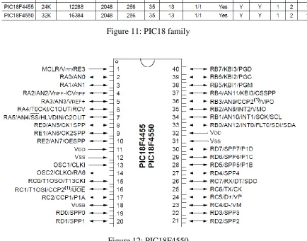
3.1.7 PIC18F4550 microcontroller
PIC is a family of modified Harvard architecture microcontrollers made by Microchip Technology. The name PIC initially referred to Peripheral Interface Controller.
PIC18F4550 is an 8-bit microcontroller of PIC18 family. PIC18F family is based on 16-bit instruction set architecture. PIC18F4550 consists of 32 KB flash memory, 2 KB SRAM and 256 Bytes EEPROM.
This is a 40 pin PIC Microcontroller consisting of 5 I/O ports (PORTA, PORTB, PORTC, PORTD and PORTE). PORTB and PORTD have 8 pins to
receive/transmit 8-bit I/O data. The remaining ports have different numbers of pins for I/O data communications.
21
Figure 11: PIC18 family
Figure 12: PIC18F4550
3.2 Software selection
C language is chosen to write the PWM program for the PIC18F4550 microcontroller. The C programming is written in MPLAB Integrated Development Environment (IDE) software. The circuit for the buck converter is designed in Proteus software.
3.2.1 MPLAB IDE
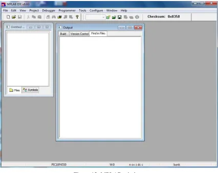
[image:31.612.118.552.143.484.2]22
[image:32.612.116.542.153.492.2]Microchip microcontrollers. It is called an Integrated Development Environment, or IDE, because it provides a single integrated environment to develop code for embedded microcontrollers. Figure 13 shows MPLAB window.
Figure 13: MPLAB window
3.2.2 Proteus
Proteus is software for microprocessor and microcontroller simulation, schematic capture, and printed circuit board (PCB) design. It is developed by Labcenter Electronics. Figure 14 shows Proteus window.
23
Capture to design the buck converter circuit and VSM mode to simulate the buck converter circuit.
[image:33.612.118.540.134.390.2]
Figure 14: Proteus window
3.3 PWM Programming
The PWM signal to drive the MOSFET is generated from PIC18F4550 microcontroller. PIC18F4550 microcontroller has two CCP (Capture/Compare/PWM) modules. These modules are used to create the PWM signal. Pin RC2 is used to output the PWM signal.
3.3.1 Capture/Compare/PWM (CCP) modules
24
The CCP modules utilize Timers 1, 2 or 3, depending on the mode selected. Timer1 and Timer3 are available to modules in Capture or Compare modes, while Timer2 is available for modules in PWM mode.
[image:34.612.154.498.263.585.2]In Pulse-Width Modulation (PWM) mode, the CCPx pin produces up to a 10-bit resolution PWM output. Since the CCP2 pin is multiplexed with a PORTB or PORTC data latch, the appropriate TRIS bit must be cleared to make the CCP2 pin an output. Figure 15 shows a simplified block diagram of the CCP module in PWM mode.
Figure 15: CCP module in PWM mode.
39
REFERENCES
[1] Dusan Gleich, Mira Milanovic, Suzana Uran, Franic Mihalic.“Digitally controlled buck converter” IEEE power electronics society ISCAS-2004, pp-V944-V947.
[2] Tarun Gupta, R.R. Boudreaux, R.M. Nelms and John Y Hung, “Implementation of a fuzzy controller for DC-DC converters using an inexpensive 8-bit
Microcontroller”, IEEE Transactions on Industrial Electronics, Vol. 44, No.5, October 1997.
[3] Trip, N. D., & Dale, S. (2010). Digital Control for Switched Mode DC-DC Buck Converters, 99–102.
[4] Gupta, T., Boudreaux, R. R., Member, S., Nelms, R. M., & Member, S. (1997). Implementation of a Fuzzy Controller for DC – DC Converters Using an Inexpensive 8-bit Microcontroller, 44(5), 661–669.
[5] R. W. Erickson and D. Maksimovic, Fundamentals of Power Electronics, 2nd ed., Norwell: Kluwer Academic Publishers, 2001.
40
[7] Geethanjali, P., Priya, P. V., Kowsalya, M., & Raju, J. (2010). Design and Simulation of Digital PID Controller for Open loop and Closed Loop Control of Buck Converter, 4333(6), 202–206.
[8] T. Beres, M. Olejar, J. Dudrik, Bi-directional DC/DC converter for hybrid battery, 14th International Power Electronics and Motion Control Conference, EPE-PEMC 2010, 78 – 81, Orhid, Macedonia
[9] K. Godbole, “Converting Analog Controllers to Smart Controllers with the TMS320C2000 DSPs,” Application Report, Texas Instruments, June 2004.
[10] Kursun, V., Narendra, S. G., De, V. K., & Friedman, E. G. (2002). Efficiency Analysis of a High Frequency Buck Converter for On-Chip Integration with a Dual-V DD Microprocessor, 2, 743–746.
[11] Starman, M., & Anwari, M. (2007). Digitally Controlled Synchronous Buck Converter, (2), 911–914.
[12] Yi, C., Wang, X., Yie, W., Tan, C., Giap, C., & Fung, Y. (2011). Buck DC-DC Converter for Embedded Control System, (October), 144–149.
[13] Mouhadjer, S., Chermitti, A., & Neçaibia, A. (2012). Comprehensive and field study to design a buck converter for photovoltaic systems, 15, 321–330.
[14] Elias, A., Junior, D., Britto, J. R. De, Freitas, L. C. De, Farias, V. J., Coelho, E. A. A., Batista, J., et al. (n.d.). MICROCONTROLLER-BASED QUADRATIC BUCK CONVERTER USED AS LED LAMP DRIVER Keywords
Acknowledgments Proposed LED Lamp Driver : Basic Operation.
41
[16] Jerome, J., & Ieee, M. (2006). Microcontroller Based Fuzzy Logic Technique for DC-DC Converter.
[17] Boudreaux, R. R., Nelms, R. M., & Hung, J. Y. (n.d.). Simulation and Modeling of a DC-DC Converter Controlled by an %bit Microcontroller, 963–969.
[18] Guo, L., Hung, J. Y., & Nelms, R. M. (2002). PID Controller Modifications to Improve Steady-State Performance of Digital Controllers for Buck and Boost Converters, 00(c), 381–388.
[19] Wang, S., Wang, M., Ma, Y., & Hong, H. (2009). Series Connected Buck-Boost Type Solar Power Converter Based on Microcontroller, 2642–2646.