ANALOGUE AND MIXED-SIGNAL TEST FOR SYSTEMS ON CHIP
Flexible embedded test solution for high-speed
analogue front-end architectures
A. Lechner, M.J. Burbidge and A.M.D. Richardson
Abstract: A flexible embedded test solution for high-speed analogue front-end subsystems is
presented. A novel concept of a flexible test solution that addresses virtual component test requirements in particular is introduced. The integration and application of the non-invasive digital test solution is demonstrated for a representative design. Its area overhead is assessed for different depths in on-chip test evaluation.
1 Introduction
For complex system-on-chip (SoC) implementations, design reuse is of crucial importance towards achieving productiv-ity and meeting time-to-market requirements. This is especially the case for analogue and mixed-signal compo-nents, as the number of analogue designers is not increasing and neither is their productivity[1]. Due to limited design engineering resources, importing third-party designs is becoming common practice for digital structures. Here, the third-party design house provides what is referred to as a virtual component to the system integrator. This is essentially a reusable design that is also commonly referred to as an IP (intellectual property) block, reflecting the fact that the IP provider retains ownership of the design IP. However, virtual component insertion involves new chal-lenges, such as tool development for reuse driven block and system characterisation, design data management and flexible functional or physical hierarchy management [2]. The main challenge for the IP provider is the design of a relatively process-independent circuit, where technology retargeting is relatively straightforward. At the same time, SoC integrators have to synchronise design schedules for both analogue and digital system components, which demands the integration of analogue and mixed-signal virtual components. Testing is predicted to be the most difficult aspect in mixed-signal design, especially for imported virtual components[3]. Testability of such virtual components has to be seen as part of the specifications guaranteed and provided with the IP block. The integration of on-chip tester functions can provide more independence from external tester resources, which is of particular interest where the analogue virtual component is integrated into a mainly digital system. However, the employed test solution has to be independent of surrounding SoC components to maintain reusability, should be scalable to similar virtual components of alternative specification and incorporate flexibility in test application and the extent of using on-chip tester functions. In other words, any test solution for a particular circuit type has to be reusable in itself, where it
can be tailored to particular design specifications, and to balance the tradeoff between implementation cost of tester functions and achieved benefits in test cost savings.
This paper presents such a flexible embedded test solution for high-speed analogue front-end subsystems containing a programmable gain amplifier and an A/D converter. This type of architecture has been targeted as it is one of the most widely used analogue and mixed-signal components embedded in mainly digital SoCs. In high-speed analogue front-ends, production test challenges are mainly seen in the increasing performance gap between the circuit-under-test (CUT) and the external tester [2]. This performance gap becomes most evident in high-speed or high-resolution interfaces, where either the speed of required data capture or the core test time is escalating.
2 Review
The built-in self-test (BIST) for analogue and mixed-signal components has been identified as one of the major requirements for the deep submicron IC test[2, 4–6]. The main advantage of BIST is to reduce test access require-ments and to address the growing performance gap between the CUT and tester by integrating tester functions on the CUT. In addition, parasitics induced from external automatic test equipment (ATE) and the demands on ATE can be reduced. Finally, analogue BIST is expected to eventually enable the use of cheaper, digital-only testers that will help with the integration of analogue virtual compo-nents, including BIST, for digital SoC applications[2]. It is expected that the SoC integrator will be able to avoid the use of expensive mixed-signal automatic test equipment. Also, for multichip modules, on-chip test support hardware is essential to migrate the test of analogue circuitry to the wafer level. It is expected that the reuse of BIST structures will significantly reduce the escalating test generation cost, test time and the time-to-market for a range of devices. Full BIST has to include both test stimulus generation and output response analysis circuitry; in the majority of cases, partial BIST approaches include output response analysis structures implemented on-chip and rely on external test stimulus generation. As mentioned above, embedded test solutions will provide an inherent flexibility in the use of on-chip and off-on-chip tester resources.
Regarding the conventional A/D converter test, device performance can be verified in terms of static performance parameters, such as offset error, gain error, differential
The authors are with the Center for Microsystems Engineering-FAS, Lancaster University, Lancaster LA1 4YR, UK
rIEE, 2004
IEE Proceedingsonline no. 20040557 doi:10.1049/ip-cds:20040557
nonlinearity (DNL) and integral nonlinearity (INL), through assessment of the transfer function. Instead of stepping a DC voltage through the converter input range, continuous signals are employed in the static performance production test. Two A/D converter test methodologies are widely in use today which measure code transition levels, namely feedback loop testing[7, 8] and histogram testing [9–14]. A/D converter performance can also be verified in terms of dynamic performance parameters, such as signal-to-noise and distortion ratio (SINAD), total harmonic distortion (THD), etc. Generally, the aim in dynamic performance parameter testing is to identify the signal components at the A/D converter output, such as the converted input signal, harmonics and random noise, and to compute performance parameters. For the majority of these parameters and for determination of signal compo-nents, a transformation from time domain to frequency domain is required and an FFT analysis is performed [11, 14]. However, in the sine wave fitting methodology[15, 16] some dynamic performance parameters can also be determined in the time domain from an A/D converter model generated to match a data record taken from a real converter. These conventional A/D converter test meth-odologies have been standardised in the ‘IEEE Standard 1241–2000 for terminology and test methods for analog-to-digital converters’[17].
Regarding a potential on-chip test solution for high-speed converters, each test technique has a number of limitations. Histogram testing, for example, does generally require a large amount of data to be stored and evaluated on-chip while requiring a long test time. For feedback loop based solutions, the oscillation around a single transition edge can be difficult to achieve due to feedback loop dynamics. Sine wave fitting will require some significant area overhead for the on-chip computation, as do FFT-based solutions. However, BIST techniques have been published for the majority of conventional A/D converter test methodologies.
BIST techniques that allow performing an FFT analysis on-chip[18, 19]rely on the availability of a DSP core. Some BIST approaches employ more defect-oriented measure-ments avoiding the extraction of converter performance parameters[20, 21]. BIST techniques for static performance parameter evaluation have been published based on the feedback loop methodology [22] and histogram testing [23, 24]. A BIST technique targeting high-resolution converters is published in [25, 26], where a polynomial fitting algorithm is employed to the converter’s ramp response to determine gain error, offset error, and second-and third-order harmonics.
3 Test requirements of high-speed analogue
front-end architecture
Previously published work by the authors describes the investigation into realistic failure modes and determination of test requirements for the analogue front-end circuitry (Fig. 1). In-depth testability analyses using fault simulation techniques have been performed on a representative analogue front-end. Fault lists were generated using inductive fault analysis [27] and included shorts, opens, floating gate transistors and gate oxide shorts. Parametric faults have been considered in the form of offset and gain deviations at internal operational amplifiers beyond the normal process spread.
For this purpose a 32-gain-set automatic gain control circuit containing adjustable gain amplifier, a reconfigurable high-pass filter and a level shifter has been studied. Further
details and results are provided in[28]. To achieve good test quality, this part of the analogue front-end requires the assessment of gain step sizes and output voltage swing. Conventionally, gain step sizes are tested based on FFT analyses performed in all gain settings. An initial on-chip test solution evaluating average analogue front-end output values for DC input signals in all gain sets is published in [29], which led to a reduction in test time by 70% without degradation in test quality. The test solution can also be extended by reconfiguration-based test stimulus generation techniques [30]. An additional testability analysis has been performed on a 6-bit folding and interpolating A/D converter. Its failure modes and test requirements are described in [31], where the severity of failure modes is analysed in terms of static and dynamic performance parameters. This particular architecture was chosen, as it allows conclusions to be drawn on the test requirements of other high-speed architectures, such as full-flash, folding, interpolating and subranging A/D converters that may or may not include internal offset compensating resistor ladders at differential amplifier outputs [32]. The test requirements for the analogue front-end can be summarised as follows:
A static performance parameter test set achieves superior test quality compared to a dynamic performance parameter test set. This is mainly attributed to untested regions of the converters transfer function in dynamic performance parameter testing (including overflow and underflow computation) and potential test escapes caused by code sparkles. The converter has to be tested for DNL, INL, gain error and monotonicity. The automatic gain control circuit requires testing of gain step sizes and its output voltage swing. The test methodology satisfying the requirements for the flexible embedded test solution is described in the following Section.
4 Test methodology
The investigation into the front-end test requirements identified potential test escapes for the adaptation of any BIST technique mentioned in Section 2. Additionally, most of these do not satisfy the virtual component test requirements, which can be summarised as follows:
embedded test solution should be scalable for particular CUT specifications
test solution that incorporates a flexible degree of on-chip tester resources allows balancing the tradeoff between area overhead and expected test cost savings
adjustable depth of testing is desirable
test solution has to be independent from surrounding components in the SoC
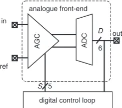
analogue front-end in
ref
AGC ADC
S 5
D
6
digital control loop out
any test solution has to be provided with some specification of achieved test quality
The test methodologies generated in this work have been based on the results of the failure mode and testability analyses. They are described separately for both analogue front-end components.
4.1
Automatic gain control circuit
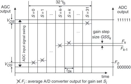
Gain step sizes can be calculated from the change in average analogue front-end output value when the gain set is incremented while a constant DC voltage is applied to the input. The test approach is illustrated in Fig. 2 (32 gain sets
are assumed). The DC voltage to apply for gain step size testing has to be determined in such a way that the automatic gain control circuit output signal (AGC output) lies within the A/D converter input signal swing for all gain sets. Offset and noise effects have to be accounted for at either end of the scale, as represented by VOS in Fig. 2. Starting at the lowest gain set (S¼0), a certain number of A/D converter output codes has to be averaged over time (F0). When the gain set has been incremented and the next
average A/D converter output (F1) is determined, the
corresponding gain step size can be calculated. The loop has to be continued until the last gain step size is calculated. This test routine is tolerant to noise effects due to the measurement of average output values for constant input voltages. The test is also tolerant to A/D converter offset effects, as the assessment of gain step sizes relies on relative (not absolute) measurements. Offset effects at the automatic gain control input can be eliminated using calibration techniques. For differential architectures, the measurement can be conducted for a positive and a negative DC input of identical absolute value. The difference in gain step sizes computed for the positive and negative DC voltages will be independent of amplifier input offset effects. The test time depends on the A/D converter speed, the number of output samples to average in each time slottsand the number of gain sets to test.
For output voltage swing testing, a similar test routine can be defined where the gain set is kept constant while a ramp stimulus is applied. The test approach is illustrated in Fig. 3, where the time slot averages are represented byFi. The ramp stimulus has to lead to an output response that extends beyond the A/D converter input signal swing to tolerate offset and noise effects (represented in Fig. 3 by
VOS). The output voltage swing can be determined by accumulating the differences in time slot averages (Dfi ). Alternatively, an approximated value can be obtained by
accumulating the number of time slots where the output average is of a certain minimum/maximum difference compared to the previous time slot’s average. The test is tolerant to noise due to the measurement of converter output averages. Offset effects can be tolerated when the ramp stimulus is defined as described above. The circuitry required for on-chip output response analysis of both, gain step size and output voltage swing test is introduced in Section 5.
4.2
A/D converter
For the A/D converter test approach, two major principles can be identified. First, to reduce test time and to avoid non-coherent sampling, the code width and INL data are computed for a single ramp input stimulus. Secondly, to achieve minimum area overhead, a small test evaluation window surrounding the converter response must be adjusted concurrently during the test sequence instead of permanently computing code occurrences over the entire A/D converter output range.
The principle of the test theme facilitating a small code count window is illustrated in Fig. 4 for a 6-bit converter. The aim is to count code occurrences in a small code region surrounding the converter’s response to a rising ramp stimulus. Code counts within a window surrounding an expected valueC(held in a 6-bit counter) are accumulated in a string of x-bit counters contained in a code count accumulator macro. Each counter in the string holds the number of occurrences for one particular code and increments its content on code identification. Assuming a chain of five x-bit counters as illustrated, the expected converter output valueCis continuously updated to adjust the code count window covered by the code count accumulator macro (C2 toC+2). For example, circuitry can be implemented within the window control macro to detect a sequence of two consecutive converter outputs (D) larger thanC. When this event occurs and the correspond-ing code count has been updated, the 6-bit counter holdcorrespond-ing
Chas to be incremented. Also, a load operation has to be instructed on the chain of x-bit counters, which effectively shifts all five code counts towards the code count sequence output. Each time such a load operation is executed, the code count previously held in counter Cnt_E can be analysed.
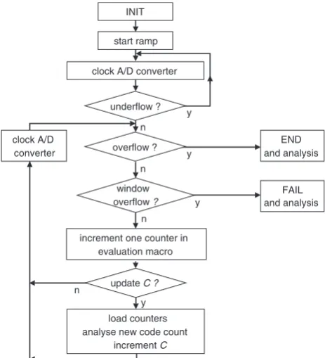
The corresponding flow chart is illustrated in Fig. 5. After test initialisation, a ramp stimulus extending beyond the input signal swing is applied to the A/D converter. The code counting initiates when the first valid converter output is detected (either non-underflow or larger than all-zero where no underflow flag is available). The window control macro’s comparator (COMP, Fig. 4) enables one of thex -bit counters to increment the corresponding code count. If time
AGC
output output ADC
ADC
input signal swing
000000 111111
tSk
gain step size GSSk
Fk-1
Fk
Fi : average A/D converter output for gain set Si
VOS
32*tS
VOS
S =
0
S =
1
S =
k-1
S = k S =
31
... ...
...
...
F0
Fig. 2 Gain step size test methodology
time AGC
output output ADC
ADC input signal swing
000000 111111
tSk
∆fk F k-1
Fk
Fi : average A/D converter output for each time slot tSi
VOS
VOS
[image:3.595.317.547.35.171.2] [image:3.595.53.279.195.340.2]the value expected for the next code count needs to be updated, the load operation and incrementing ofCneeds to be executed. The completed code count can be analysed. This loop continues until the end of the conversion range is detected, either in the form of an overflow flag or the all-one output (where no overflow computation is implemented). During the test, the window control macro sets a window overflow flag if the converter output D leaves the code count window. The test can be aborted, as test failure is computed. Reasons for window overflow can be found in non-monotonic behaviour, code sparkles or excessive INL.
Regarding the design of an embedded window control macro and code count accumulator macro, the embedded
test solution has some key specifications to adapt the test routine to particular A/D converters. Compared to Fig. 4, the number of bits in the code counters, the number of code counters in the code count accumulator macro and the complexity of the required comparator in the window control macro do not only have a major influence on area overhead but also to enable tailoring of the structure to the converter under test. The size of the code count window is determined by the number of counters in the code count accumulator macro. The size of the counters within that macro limits the number of code occurrences that can be accumulated. The required size of the code count window is mainly influenced by the extend to which noise effects have to be tolerated at the converter output. Higher-resolution converters, for example, may exhibit noise levels in excess of 1 LSB, which can require the code count window to cover more than five codes. To maintain test accuracy, the input stimulus slope can be decreased to effectively increase the ideal code counts and improve noise averaging. In such cases the window control macro needs to assess a running average of the converter output to determine when the code count window has to be adjusted. Obviously the test stimulus accuracy requirements will become more stringent. The converter’s DNL test threshold and the required measurement accuracy have a major impact on the size of the code counters. Assuming a DNL test threshold of 71 LSB, a measurement resolution of 0.2 LSB and an ideal ramp stimulus, 4-bit counters have to be implemented to compute code counts ranging from 0 to 15. The ramp stimulus has to lead to eight code counts in the ideal case. Obviously these are also the key parameters that determine the kernel test time for a single ramp test evaluation, as discussed in Section 6. If the test stimulus is generated on-chip using techniques described in [30] or can only be applied through the automatic gain control block, fault masking can be avoided by evaluating A/D converter tests in more than one gain set. However, for the devices studied in this work the potential for such fault masking is negligible, not only due to process and defect statistics but also due to the different failure modes exhibited by either block.
C 6
D
6
A/D
converter
COMP D <C-2 D =C-2 D =C-1 D =C
D =C +1
D =C +2
D >C +2
window control macro
x-bit counters with common clock but separate enable signals supplied by the window control macro
A load operation will be instructed on all x-bit counters when the value of C (expected output code) is incremented in the window control macro
code count accumulator macro
code count sequence
Cnt_A x-bit
[0]
[1]
[:]
[x-1]
[0]
[1]
[:]
[x-1]
[0]
[1]
[:]
[x-1]
[0]
[1]
[:]
[x-1]
[0]
[1]
[:]
[x-1] 0
0
:
0 6-bit
CNT
Cnt_B x-bit
Cnt_C x-bit
Cnt_D x-bit
Cnt_E x-bit
window overflow
time A/D converter ramp response
converter output
D
code count window surrounding A/D converter output
:
Fig. 4 A/D converter test methodology
INIT
start ramp
clock A/D converter
y n
y
END and analysis n
n
n clock A/D
converter
FAIL and analysis y
increment one counter in evaluation macro
y load counters analyse new code count
increment C underflow ?
overflow ?
window overflow ?
update C ?
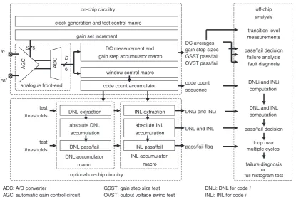
[image:4.595.54.541.25.272.2] [image:4.595.50.282.324.579.2]5 Flexible embedded test solution
The integration of the test methodology into a flexible embedded test solution and its general application is described in this Section, followed by some information on the application to a particular analogue front-end.
5.1
Application of test methodology and
implementation of flexibility
The flexible embedded test solution for high-speed analogue end circuits needs to be scalable for particular front-end circuit specifications, such as the resolution of the A/D conversion. To satisfy the requirements for testable analogue virtual component design, the test solution also has to provide some flexibility to balance the tradeoff between implementation cost and test cost savings. This Section presents the flexible embedded test solution at a functional level. The test solution’s features for A/D converter testing are described first followed by the automatic gain control testing capabilities.
The A/D converter test approach has been introduced in the previous Section. However, the test evaluation itself needs to be defined in more detail. The strategy described in this Section provides a high degree of flexibility in the implementation and application of the embedded test solution. The window control macro and the code count accumulator macro (Fig. 4) implement a code count computation on-chip. As known from conventional histo-gram testing, the code counts support the calculation of static performance parameters. Figure 6 provides an illustration of the embedded test solution’s flexibility in implementation and application.
In its most basic form, the A/D converter test approach can be realised on-chip as outlined above where code counts are computed within the on-chip code count accumulator macro. When the code count window is updated and new code count data is available, data can be captured for processing in off-chip tester resources to extract the particular code’s DNL and INL. Accumulation and
computation of maxima in these values yield absolute DNL and INL which can be compared to test thresholds for pass/fail decisions. In situations where the extracted values fall onto the pass/fail boundary, multiple ramp sections may be applied to the A/D converter to accumulate conventional histogram data sets off-chip.
Alternatively, the code count analysis can be implemen-ted on-chip, in the form of a DNL and an INL accumulator macro. This provides a test solution even more independent of external tester resources and avoids future problems caused by the growing performance gap between ATE and CUT. The functionality within these macros can range from simple DNL and INL extraction for each separate code (off-chip computation of absolute DNL/INL, comparison to thresholds etc.) to an on-chip comparison of absolute DNL/INL to test thresholds. Multiple ramp tests may be applied to the CUT in any particular implementation.
For gain step size and output voltage swing testing of an automatic gain control circuit an optional dedicated DC measurement and gain step accumulator macro is included (Fig. 6). Generally speaking this macro allows the calcula-tion of the average A/D converter output over a number of samples by employing an integration process. Furthermore the macro can include circuitry to compare two measured averages to each other, extract the difference and compare that difference to test thresholds. These analysis steps are required for gain step size testing and the assessment of the output voltage swing. The functionality is identical to the circuitry presented in [29]. However, an implementation with significantly lower area overhead has been designed. In addition to the macros mentioned so far, a clock generation and test control macro has to be added.
The execution of the A/D converter test is illustrated for an ideal device in Fig. 7. The upper plot illustrates the converter output Dand the expected valueC for a small ramp stimulus section. In this example, the value for Cis incremented when two consecutive A/D converter output samples are larger than its current value. The shaded area surrounding both curves represents the code range covered
analogue front-end in
ref
AGC ADC
S 5
ADC: A/D converter
AGC: automatic gain control circuit D
6
DC measurement and gain step accumulator macro
window control macro
DNL extraction INL extraction
absolute DNL accumulation
absolute INL accumulation DNL pass/fail INL pass/fail DNL accumulator
macro
INL accumulator macro gain set increment
clock generation and test control macro
test thresholds
test thresholds
DC averages gain step sizes GSST pass/fail OVST pass/fail
code count sequence
DNLi and INLi
DNL and INL
pass/fail flag on-chip circuitry
optional on-chip circuitry
code count accumulator
off-chip analysis transition level measurements pass/fail decision
failure analysis fault diagnosis
DNLi and INLi computation
DNL and INL computation
pass/fail decision loop over multiple cycles
failure diagnosis or full histogram test GSST: gain step size test
OVST: output voltage swing test
DNLi: DNL for code i INLi: INL for code i
[image:5.595.92.508.477.754.2]by the code count window. The A/D converter clockCais depicted below, as well as the clock signal Cc generated within the clock generation macro and supplied to the code count accumulator macro. Note that two clock pulses occur within one A/D converter clock period. While the first clock pulse controls the code counting process, the second pulse is used to trigger the load operation in the code count accumulator macro. At the bottom of the diagram the code counting and counter loading progress is illustrated for five counters (Cnt_AtoCnt_Eas in Fig. 4). Within each A/D converter clock period, one counter is incremented. In the illustrated ideal case this is mostly counterCnt_Cwhen the converter output is of the expected value (D¼C). ALOAD
signal becomes active when two consecutive converter outputs are larger than the expected value. As a result, code counts are shifted towards the code count sequence output. This data is available for code width, DNL and INL computation.
The implementation of the flexible embedded test solution is described in the following Section using the maximum degree of on-chip tester resources for DNL and INL accumulation, indication of missing bins and non-monotonicity, gain step size testing and output voltage swing assessment.
5.2
Implementation and application of the
test solution
[image:6.595.140.460.35.243.2]The on-chip tester macros required for the evaluation of the analogue front-end test set have been introduced above. A more detailed block diagram is provided in Fig. 8. In this particular case, the flexible embedded test solution has been designed for an analogue front-end containing a 32-gain-set automatic gain control circuit and a 6-bit A/D converter. Details of the analogue front-end originally analysed in [28, 31]and the designed test solution are listed in Table 1. Apart from the indication of window overflow discussed above, the designed circuitry also indicates overflow in DNL and INL computation and allows test application for both rising and falling ramp stimulus sections.
The flexible embedded test solution illustrated in Fig. 8 has been designed at gate level. Digital XSPICE models for a standard CMOS process were used. A particular process was selected to match the folding and interpolating A/D converter technology. Simulation results show that the
designed embedded test solution has a maximum clock frequency of 330 MHz (identical to the maximum converter sampling frequency). Some simulation results are presented in the following Section.
The area overhead for the test solution with maximum on-chip tester capabilities is equivalent to 1214 standard CMOS two-input NAND gates. The area overhead contribution is identified for each test solution macro in Fig. 9. Clock generation circuitry and macros to control the test routines account for 32% (387 gates) of the maximum area overhead. If a minimum degree of on-chip tester hardware is selected that computes the code count sequence only, the overall area overhead corresponds to 691 gates. The on-chip extraction of DNL and INL data requires an additional 314 gates. Circuitry for automatic gain control tests accounts for 17% of the maximum area overhead. Test times and simulation results are provided in the following Section.
6 Simulation results
To test the automatic gain control block for gain step sizes, a DC voltage is applied to the primary analogue front-end input. Starting at the lowest gain set, the DC measurement and gain set accumulator macro integrates a defined number of A/D converter output codes at maximum clock speed. In the particular simulation illustrated in Fig. 10, 6-bit converter outputs are integrated to form the 10-bit average accumulated in latch A (Fig. 8). The 10-bit average therefore provides a measurement resolution of 0.0625 LSB and dithering techniques can be employed to achieve this resolution. When a gain set’s average has been computed, the difference from the previous gain set’s average output is calculated in a 10-bit adder. The test signature GSno is incremented when the gain step size is of a certain minimum size and the latest average is moved to latch B. The test is completed when all gain step sizes have been determined. The test signature for good devices with 32 gain sets is provided as a pass/fail flag (GSpass). The plot for the content of latch A (LaA in Fig. 10) illustrates the accumulation of output averages for all 32 gain sets while latch B (LaB in Fig. 10) provides the previous gain set’s average. In the ideal case, the test signature GSno is incremented with each gain set from 0 to 31.
[binary] 001001 001000 000111 000110 000101 000100 000011
eight samples/ code D > C
time
D (A/D converter output)
C (expected value)
code count window (for five 4-bit counters)
A/D converter sample points Ca : A/D sample clock)
Cc : count and load clock
LOAD : enable for counter load
0 0 0 0 0 0 0 0 0 0 0 0 0 0 0 0 0 0 0 0 0 0 0 Cnt_A (D = C+2) 5-bit 0 1 2 0 0 0 0 0 0 1 2 0 0 0 0 0 0 1 2 0 0 0 0 Cnt_B (D = C+1) counter 8 8 8 3 4 5 6 7 8 8 8 3 4 5 6 7 8 8 8 3 4 5 6 Cnt_C (D = C) content in 8 8 8 8 8 8 8 8 8 8 8 8 8 8 8 8 8 8 8 8 8 8 8 Cnt_D (D = C-1) decimal 8 8 8 8 8 8 8 8 8 8 8 8 8 8 8 8 8 8 8 8 8 8 8 Cnt_E (D = C+2) notation
8 8 8 code count sequence
(available for analysis) code count
for 000011
code count for 000100
code count for 000101
Compared to the block diagram in Fig. 8, the DC measurement and gain set accumulator macro has been designed using only one 10-bit adder that is reconfigured for average accumulation and gain step size calculation. With
the reconfiguration of the 10-bit adder, the test time can be determined as follows: 16 clock periods are required for average accumulation and four additional clock periods have to be spent on the calculation of the difference in DNLovf
window control macro
INL accumulator macro
D<
0: 5
>
Ca
clock generation macro A
Enadc : enable for A/D converter test
Ca,Cb: ADC and inverted clock Cc : code count accumulator clock Ce,Co : evaluation, comparator clock LOAD : enable signal for loading Rt : test reset signal
Wovf : window overfow flag
CC_data : accumulated code counts
CC_ideal : ideal code count
DNL: absolute DNL (4-bit)
DNLi : DNL of code i (4-bit)
DNLovf : overflow in DNL INL: absolute INL (6-bit)
INLi : INL of code i (6-bit)
INLovf : overflow in INL
delay Cb Cc Co Ce LOAD CC_data
code count accumulator macro
CC_data CC_ideal 4bit Cnt_A Rt Cc EN LOAD Wovf p0 P<Q p1 P = Q-2 p2 P = Q-1 p3 P = Q p4 P = Q+1 p5 P = Q+2 P >Q q0 q1 q2 q3 q4 q5 6bit COMP Co Rt Cc 1bit DFF
delay (1/4*TCa)
Rt Co 1bit DFF d0 q0 q0 q1 q2 q3 q4 q5 Rt Cc EN 6bit CNT1 d0 q0 d1 q1 d2 q2 d3 q3 4bit Cnt_B Rt Cc EN LOAD d0 q0 d1 q1 d2 q2 d3 q3 4bit Cnt_C Rt Cc EN LOAD d0 q0 d1 q1 d2 q2 d3 q3 4bit Cnt_D Rt Cc EN LOAD d0 q0 d1 q1 d2 q2 d3 q3 4bit Cnt_E Rt Cc EN LOAD d0 q0 d1 q1 d2 q2 d3 q3
code_C+2 code_C+1 code_C c ode_C-1 code_C-2
1 Rt Ce Cin 4bit ADD DNLi DNL 6bit ADD 6bit COMP 4bit COMP C< 0:5> 4bit DFF Rt Ce 4bit DFF Rt Ce EN INLi 6bit DFF Rt Ce 6bit DFF Rt Ce EN INL INLovf p0 p1 p2 |P|>|Q| p3 q0 q1 q2 q3 p0 dovf p1 p2 p3 d0 q0 d1 q1 d2 q2 d3 q3 d0 q0 d1 q1 d2 q2 d3 q3 d0 q0 d1 q1 d2 q2 d3 q3 p0 s0 p1 s1 p2 s2 p3 s3 p4 s4 p5 s5 q0 q1 q2 q3 q4 q5 sovf d0 q0 d1 q1 d2 q2 d2 q3 d4 q4 d5 q5 d0 q0 d1 q1 d2 q2 d3 q3 d4 q4 d5 q5 p0 |P|>|Q| p1 p2 p3 p4 p5 q0 q1 q2 q3 q4 q5
DNL accumulator macro d0 q0
ENadc
LOAD
DC measurement and gain set accumulator macro Cla: clock identical to Ca (when enabled)
Clb: clock in ratio of 1:16 to Cla Rla: reset to integrator latch
C< 0:5>: A/D converter output
T< 0:9>: integral of C over 16 codes
U< 0:9>: integral of previous 16 codes
V< 0:9>: difference between integralsT and U
GSno< 0:4>: number of passed gain step sizes
GSpass: pass flag for gain step size test D<
0:5 > 1 Cin 10bit ADD p0 s0 : : : : p9 s9 sovf q0 : : q9 Rla Cla 10bit DFF d0 q0 : : : : d9 q9 Cin 10bit ADD p0 d0 : : : : p9 d9 dovf q0 : : q9 Rt Clb 10bit DFF d0 q0 : : : : d9 q9 0 S< 0:9 > T< 0:9> U< 0:9 > V< 0:9 > Ca ENagc Cla Clb Rla 4bit Cnt_B d0 q0 : : d3 q3 qovf Rt Cla delay
clock generation macro B
Rla Cib 5bit CNT d0 q0 q4 qovf GSno< 0:4 > GSpass latchA latchB
[image:7.595.51.542.34.670.2]averages. Therefore, the gain step test time tGSST can be given as
tGSST ¼
GS fS
ðNSþ4Þ ð1Þ
wherefSis the maximum A/D conversion rate,GS is the number of gain sets andNSis the number of A/D converter outputs to average for each gain set. For the representative design, withfS¼330 MHz,GS¼32 and NS¼16, the test time results to 1.94ms.
In output voltage swing tests, the DC measurement and gain step accumulator macro performs a similar algorithm
while the gain set is kept constant and a ramp stimulus is applied to the primary input of the analogue front-end. The computed test signature GSnocorresponds to the number of time slots with a verified minimum difference compared to the previous time slot’s average. The output voltage swing test timetOVSTcan be given as:
tOVST ¼
TS fS
ðNSþ4Þ ð2Þ
where fSis the maximum A/D conversion rate,TS is the number of time slots covered by the ramp response andNS is the number of A/D converter outputs to average for each time slot. For the representative design, withfS¼330 MHz,
TS¼32 andNS¼16, the test time results to 1.94ms. The A/D converter ramp test approach has been introduced above. Simulation results for the representative analogue front-end circuit are illustrated in Fig. 11, where the upper graph shows the A/D converter outputDand its expected value C. The ramp input stimulus is defined to extend into converter underflow and overflow and to lead to an ideal code count of eight for all 64 code bins. The shaded region surrounding the staircase waveform for C
[image:8.595.48.549.47.210.2]represents the code count window that allows computation of codes occurring in the range from C2 toC+2. Each time the expected valueCis incremented, the load operation is performed on all code counters and one code count value becomes available for analysis. The bottom graph illustrates the generated code count sequence available for DNL and INL computation at the output of the code count accumulator macro (CC_data in Fig. 8). When A/D
Table 1: Specifications for flexible embedded test solution
Parameter name Parameter Value Description and comments
A/D converter resolution N 6 number of bits
Sampling frequency fS 330 MHz maximum A/D converter frequency
Number of gain sets GS 32 number of gain sets in the automatic gain control circuit
DNL test threshold DNL 70.5 LSB as determined for representative design
INL test threshold INL 71 LSB as determined for representative design
Ideal code count CC_ideal 8 ideal code width in number of samples for ramp stimulus used in A/D converter test
DNL measurement range 1 LSB to 0.875 LSB range before DNL overflow occurs
INL measurement range 4 LSB to 3.875 LSB range before INL overflow occurs
DNL/INL resolution 70.2 LSB accuracy of code count/width computation
Maximum noise level 1 LSB maximum amplitude of acceptable noise effects
window control and gain set macros 20%; 240
clock generation and test control macro
12%; 147
code count accumulator macro 25%; 304
DNL accumulator macro
7%; 88 INL accumulator
macro
19%; 226 DC measurement and gain set accumulator macro
17%; 209
Fig. 9 Area overhead (in two-input NAND gate equivalents)
time, µs
0.0 0.5 1.0 1.5 2.0
GSno [decimal]
31
20
0
LaA
[image:8.595.50.280.250.404.2] [image:8.595.135.465.608.759.2]LaB
[binary]
1111000000
1010000000
0101000000
0000000000
clock latches A and B
latch A holds difference in gain set integrals GSno
GSpass
LaA LaB
G Spass Pass flag
LaB: content latch B (previous gain set integral) LaA: content latch A
(current gain set integral and difference)
GSNO
(number of passed gain step sizes)
converter overflow is detected and the test is completed, the code counts for the three highest converter bins need to be shifted out of the code counter chain. The plot illustrates 64 code counts equal to eight.
The A/D converter single ramp test time tSRT can be given as
tSRT ¼
ð2Nþ2OSÞ CC ideal
fS
ð3Þ
wherefSis the maximum A/D conversion rate,CCidealis the ideal code count corresponding to 1 LSB, N is the resolution of the converter andOSis the extend of offset in LSB to tolerate (at either end of the ramp stimulus). For the representative design, withfS ¼330 MHz,OS¼1 LSB andCCideal ¼ 8, the test time for a single ramp stimulus results to 1.6ms.
Failure mode detection capabilities have been assessed through simulation. Typical failure modes, some of which are discussed in[31], were modelled within the input stimuli to the ideal converter model. Figure 12 illustrates the code count sequence, DNL and INL computation for a converter suffering from nonlinearity in the centre of its input range. Such failure modes affecting a region of output codes can be exhibited by interpolating converters in particular. Fault F27 is chosen here, as it is an example for a more difficult to detect failure mode with DNL values well within the tolerance window. The test evaluation (Fig. 12) allows clear identification of the fault-affected code region in the centre of the input voltage swing, where code widths decrease to a lowest count of five. The region of codes with a small negative DNL leads to the computation of a detectable absolute INL of –1.75 LSB. This kind of failure mode can be exhibited by other converter architec-tures employing compensation resistor ladders. However, where such structures are not included, similar underlying
faults will have a harder effect on the code width of one particular code easily extracted as DNL failure.
Table 2 provides a summary of test results obtained from the application of the flexible embedded test solution to a selection of failure modes. The ‘window overflow’ column lists whether a fault leads to code count window overflow. Where this is the case, the test will normally be aborted without further analysis of other test results. Similarly, nonlinearity overflow in DNL and/or INL will result in test abortion. The three following columns list the measured values for absolute DNL and INL in LSB and indicate whether a missing bin is detected. The last column states if the particular failure mode passes the test.
Catastrophic failure modes (Gr. 3) are all detected due to overflow in the code count window. Faults F210, F219 and F249 are examples for potential test escapes in conventional dynamic performance tests, as they cause failure in untested regions of the transfer function and difficult to detect code time, µs
time, µs
0 0.2 0.4 0.6 0.8 1.0 1.2 1.4 1.6
C
expected value 111100
101000
010100
000000
D
A/D converter output
D
C
code count window ranges from C -2 to C +2
[image:9.595.132.464.33.330.2] [image:9.595.314.547.377.523.2]0 0.2 0.4 0.6 0.8 1.0 1.2 1.4 1.6
[binary]
[binary]
1000
0000
code count sequence captured at counter E on shift operation
code count shift operations three remaining code counts at end of test
Fig. 11 Simulation for ideal A/D converter
0 0.2 0.4 0.6 0.8 1.0 1.2 1.4 1.6
CC
[decimal]
8
4
0
DNLi INLi CC : code count sequence code count sequence
time, µs
INLi DNLi
DNL/
INL,
LSB
20/8 10/8 0
−10/8
−20/8
−30/8
sparkles. Less severe failure modes, where no window overflow is caused (Gr. 2), are mostly detected by INL measurements evaluated on-chip. However, this is due to the spreading of failure modes caused by interpolation and other compensation resistor ladders. In converter architec-tures that do not include such functions, the failure mode will remain restricted to one or two adjacent bins leading to significantly higher DNL. Where the failure mode is even softer (Gr. 1), fault detection depends on the test thresholds applied to the particular design. The absolute INL computed for faults F276 and F278, for example, is right at the boundary of the pass/fail decision, while the DNL is slightly beyond the normal process spread. These faults are detected for the representative design. In Table 2, however, they have not been classified as generally detected. Gain errors are generally detectable in INL measurements.
7 Conclusions and future work
A flexible embedded test solution for high-speed analogue front-end circuits has been presented. The novel concept of a flexible test solution that addresses virtual component test requirements in particular has been discussed. The non-invasive test solution has been designed for a representative analogue front-end circuit. Its area overhead has been assessed for different depths in on-chip test evaluation.
Test results are generated in the form of average A/D converter output for DC measurements and pass/fail flags for gain step size tests and output voltage swing tests. Additionally, code count sequences for off-chip analysis, DNL and INL sequences and absolute values are provided as well as the gain error and flags for missing bins and non-monotonic behaviour. The test solution can be used for single rising/falling ramp A/D converter test and for test data compression in conventional full-histogram tests (supported by further off-chip data accumulation and analysis). The test solution is generically applicable to analogue front-end sub-systems and achieves largest benefit for high-speed architectures.
As test signatures are extracted on-chip, the test solution prevents one of the major bottlenecks in analogue high-speed circuit test, the performance gap between CUT and ATE. The purely digital embedded test solution also has advantages compared to conventional circuit testing, ranging from the use of digital standard access structures to an automatic synthesis of on-chip tester functions.
The results of testability analyses performed on repre-sentative analogue front–end components [28, 31]and the interpretation of these for other high-speed architectures [32]provides evidence for superior test quality compared to conventional FFT-based testing. The kernel test time for the programmable gain block is reduced significantly while more time-consuming data capturing is avoided in A/D converter testing.
Future work will address the incorporation of test stimulus generation techniques and assessment of accuracy requirements. Further work is required for automatic generation and scaling of the test solution for particular designs, specifications, stimulus accuracy, test thresholds, available silicon area and acceptable test time. Additionally, similar flexible embedded test solutions are required that address high-resolution A/D converter testing.
8 Acknowledgments
This work has been supported by EPSRC through the ‘ATOM’ project (Analogue and Mixed Signal Integrated Circuit Test Support for High Quality, Low Cost Manufacture) - EPSRC GR/M7553, through EC Frame-work 4 program ‘ASTERIS’ ref: ESPRIT 26354 and the EC Framework V program ‘TAMES-2’ IST-2001-34283.
9 References
1 Nandra, N.: ‘Analogue synthesis for SoC’, Electron. Syst. Softw., 2003,1, (4), pp. 16–19
2 Semiconductor Industry Association: ‘International technology road-map for semiconductors’. 2001 edn., and 2002 update, 2002 3 Nagi, N.: ‘System-on-a-chip mixed-signal test: issues, current industry
practices and future trends’. Proc. Int. Mixed Signal Testing Work-shop, IMSTW99, Whistler, British Columbia, Canada, 15–18 June 1999, pp. 201–211
4 Arnold, B.: ‘Built-in self-test gains ground as ATE time and cost soar’,
Electron. Des., 2000,48, (19), pp. 117–124
5 Sunter, S.: ‘Mini tutorial: mixed signal test’. Presented at 7th IEEE Int. Mixed-Signal Testing Workshop, IMSTW01, Atlanta, GA, USA, 13– 15 June 2001
6 Sunter, S.: ‘Tutorial: Mixed-signal BIST - does industry need it?’. Presented at 3rd IEEE Int. Mixed Signal Testing Workshop, IMSTW97, Seattle, Washington, USA, 3–6 June 1997
7 Corcoran, J.J., Hornak, T., and Skov, P.B.: ‘A high resolution error plotter for analog-to-digital converters’,IEEE Trans. Instrum. Meas., 1975,IM-24, (4), pp. 370–374
8 Max, S.: ‘Optimum measurement ADC transitions using a feedback loop’. Proc. 16th IEEE Conf. on Instrumentation and Measurement Technology, Venice, Italy, 24–26 May 1999, pp. 1415–1420 9 Pretzl, G.: ‘Dynamic testing of high speed aid converters’,IEEE J.
Solid-State Circuits, 1978,13, pp. 368–371
[image:10.595.45.554.47.227.2]10 Doernberg, J., Lee, H.S., and Hodges, D.A.: ‘Full-speed testing of A/ D converters’,IEEE J. Solid-State Circuits, 1984,19, (6), pp. 820–827 Table 2: Test results for a selection of representative failure modes
Faults Window overflow Nonlinearity overflow DNL [LSB] INL [LSB] Missing bin Pass test
Fault free 0 0 0 0 0 yes
Gr. 1 F27 0 0 0.375 1.75 0 no
F276 0 0 0.75 1 0 yes/no
F278 0 0 0.625 1.125 0 yes/no
Gr. 2 F77 0 0 0.875 3.25 0 no
F78 0 0 0.875 2.875 0 no
F356 0 DNL/INL 0.875 1.125 1 no
Gr. 3 F21 1 INL 0.875 +3.5 0 no
F112 1 DNL/INL 0 0 0 no
F210 1 0 0 0 0 no
F219 1 0 0 0 0 no
11 Mahoney, M.: ‘DSP-based testing of analog and mixed-signal circuits’ (IEEE Computer Society, USA, 1987)
12 Blair, J.: ‘Histogram measurement of ADC nonlinearities using sine waves’,IEEE Trans. Instrum. Meas., 1994,43, (3), pp. 373–383 13 Max, S.: ‘Testing high speed high accuracy analog to digital converters
embedded in systems on a chip’. Proc. IEEE Int. Test Conf., Atlantic City, NJ, USA, 28–30 Sept. 1999, pp. 763–771
14 Burns, M., and Roberts, G.W.: ‘An introduction to mixed-signal IC test and measurement’ (Oxford University Press, UK, 2001) 15 Peetz, B.E.: ‘Dynamic testing of waveform recorders’,IEEE Trans.
Instrum. Meas., 1983,32, (1), pp. 12–17
16 Linnenbrink, T.: ‘Effective bits: is that all there is?’,IEEE Trans. Instrum. Meas., 1984,IM-33, (3), pp. 184–187
17 IEEE Standard 1241-2000: ‘IEEE standard for terminology and test methods for analog-to-digital converters’. Institute of Electrical and Electronics Engineers Inc., 2000
18 Toner, M.F., and Roberts, G.W.: ‘A frequency response, harmonic distortion test for BIST of a sigma-delta ADC’,IEEE Trans. Circuits Syst. II, Analog Digit. Signal Process., 1996,43, (8), pp. 608–613 19 Teraoka, E., Kengaku, T., Yasui, I., Ishikawa, K., Matsuo, T., and
Wakada, H.: ‘Built-in self-test for ADC and DAC in a single-chip speech CODEC’,IEICE Trans. Fundam. Electron. Commun. Comput. Sci., 1997,e80a, (2), pp. 339–345
20 Mir, S., Lubaszewski, M., and Courtois, B.: ‘Unified built-in self-test for fully differential analog circuits’,J. Electron. Test., Theory Appl., 1996,9, (1–2), pp. 135–151
21 Mir, S., Rueda, A., Huertas, J.L., and Liberali, V.: ‘A BIST technique for sigma-delta modulators based on circuit reconfiguration’. Proc. 3rd IEEE Int. Mixed Signal Testing Workshop, IMSTW97, Seattle, WA, USA, 3–6 June 1997, pp. 179–184
22 Arabi, K., and Kaminska, B.: ‘Oscillation built-in self test (OBIST) scheme for functional and structural testing of analog and mixed-signal circuits’. Proc. IEEE Int. Test Conf., ITC97, Washington, DC, USA, 3–5 Nov. 1997, pp. 786–795
23 Frisch, A., and Almy, T.: ‘HABIST: histogram-based analog built in self test’. Proc. IEEE Int. Test Conf. ITC97, Washington, DC, USA, 3–5 Nov. 1997, pp. 760–767
24 Aza.ıs, F., Bernard, S., Bertrand, Y., and Renovell, M.: ‘Implementa-tion of a linear histogram BIST for ADCs’. Proc. Design, Automa‘Implementa-tion and Test in Europe, DATE01, Munich, Germany, 13–16 March 2001, pp. 590–595
25 Sunter, S.K., and Nagi, N.: ‘A simplified polynomial-fitting algorithm for DAC and ADC BIST’. Proc. IEEE Int. Test Conf., ITC97, Washington, DC, USA, 3–5 Nov. 1997, pp. 389–395
26 Roy, A., Sunter, S., Fudoli, A., and Appello, D.: ‘High accuracy stimulus generation for A/D converter BIST’. Proc. IEEE Int. Test Conf., ITC02, Baltimore, MD, USA, 8–10 Oct. 2002, pp. 1031–1039 27 Sachdev, M., and Atzema, B.: ‘Industrial relevance of analog IFA: a fact or a fiction’. Proc. IEEE Int. Test Conf., ITC95, Washington, DC, USA, 21–25 Oct. 1995, pp. 61–70
28 Lechner, A., Richardson, A., Hermes, B., and Ohletz, M.: ‘A design for testability study on a high performance automatic gain control circuit’. Proc. 16th IEEE VLSI Test Symp., VTS98, Monterey, CA, USA, 26–30 April 1998, pp. 376–385
29 Lechner, A., Ferguson, J., Richardson, A., and Hermes, B.: ‘A digital partial built-in self-test for a high performance automatic gain control circuit’. Proc. Design, Automation and Test in Europe, DATE99, Munich, Germany, 9–12 March 1999, pp. 232–238
30 Lechner, A., Richardson, A., and Hermes, B.: ‘Reconfiguration-based built-in self-test for analogue front-end circuits’. Proc. 5th IEEE Int. Mixed Signal Testing Workshop, IMSTW99, Whistler, Canada, 15– 18 June 1999, pp. 243–247
31 Lechner, A., Richardson, A., and Hermes, B.: ‘Short circuit faults in state-of-the-art ADCs - are they hard or soft’. Proc. 10th Asian Test Conf., ATS01, Kyoto, Japan, 19–21 Nov. 2001, pp. 417–422 32 Lechner, A.: ‘Flexible embedded test solution for high-speed analogue