International Journal of Emerging Technology and Advanced Engineering
Website: www.ijetae.com (ISSN 2250-2459,ISO 9001:2008 Certified Journal, Volume 4, Issue 1, January 2014)
216
Design and Implementation of 16-bit Ripple Carry Adder for
Low Power in 45nm CMOS Technology
Dhara D. Joshi
1, Prof. Jai Karan Singh
21,2
Department of electronics & Communication, Sri Satya Sai Institute of Science & Technology, Bhopal, MP, India,
Abstract— This paper will represent the design and implementation of 16 bit ripple carry adder(RCA), using three different CMOS topology as static or conventional CMOS, Gate diffusion input(GDI) and Adiabatic technology. Adder is the basic building for all arithmetic operations like addition, subtraction. we have implemented the 16 bit ripple carry adder in BPTM 45nm CMOS technology in LT spice IV.
Keywords—CMOS, GDI, RCA, BPTM, Adiabatic.
I. INTRODUCTION
Power consumption and it’s minimization is one of the primary concerns in today VLSI design methodologies because of two main reasons one is the long battery operating life requirement of mobile and portable devices and second is due to increasing number of transistors on a single chip leads to high power dissipation and it can lead to reliability and IC packaging problems.
Adiabatic logic reduces the energy dissipation by reducing the dissipation across resistances of conducting MOSFETs and recovering the part of energy given to the output back to the source, which extends the battery life. Several adiabatic logic styles are available but here we implemented 1n-1p Quasi adiabatic logic. As we know Full adders are important components in applications such as digital signal processors (DSP) architectures and microprocessors. Apart from the basic addition adders also used in performing useful operations such as subtraction, multiplication, division, address calculation, etc.
II. CONVENTIONAL CMOSLOGIC,ADIABATIC LOGIC AND
GDILOGIC
A. Conventional CMOS Logic
The dominant factor of power dissipation in a conventional CMOS device is the dynamic power required to charge and discharge the capacitive nodes within the circuit itself. To charge the node capacitance CL from a dc supply of potential VDD, an energy
……….(1)
Is withdrawn from supply. Only half of this energy is temporarily stored in capacitor CL. The remaining
………(2)
Is dissipated as heat in the on resistance of PMOS. When input becomes logic high, the NMOS turns on and energy stored on capacitor CL is discharged to the ground and dissipated as heat. Hence during a complete charge- discharge cycle, the energy
……….(3)
Is withdrawn from power supply and is dissipated as heat. Half of this energy is dissipated during charging and half is dissipated during discharging.
B. Adiabatic Logic
In static CMOS logic, the abrupt application of supply voltage gives rise to high potential across the switching device. The energy dissipation during charging and discharging can be minimized to a great effect by ensuring that the potential across switching device is kept sufficiently small. Adiabatic charging may be achieved by charging the capacitor from a time varying source that starts at 0V. This time varying source rises towards V at a slow rate that ensures that potential across switching device is kept arbitrarily small. The adiabatic charging is shown in figure 1.
In fact the energy dissipated across the resistance, R is
…………..(4)
From the above equation (4), we can see that if T >> RC, the energy dissipation during charging Ediss ≈ 0. Same is applicable during discharge process. In addition to this, in some adiabatic logics, the energy dissipation also occurs due to threshold voltage of MOSFET and diode cut-in voltage. The energy dissipation due to threshold voltage Vt is
………..(5)
The energy dissipation due to diode cut-in voltage Vd is
International Journal of Emerging Technology and Advanced Engineering
Website: www.ijetae.com (ISSN 2250-2459,ISO 9001:2008 Certified Journal, Volume 4, Issue 1, January 2014)
[image:2.612.56.287.138.270.2]217 Where, Vs is the voltage swing.
Figure 1 Adiabatic charging
C. GDI Logic
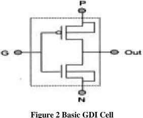
A new low power design technique that solves most of the problems known as Gate-Diffusion-Input (GDI) is proposed. This technique allows reducing power consumption, propagation delay, and area of digital circuits. A basic GDI cell contains four terminals – G (common gate input of nMOS and pMOS transistors), P (the outer diffusion node of pMOS transistor), N (the outer diffusion node of nMOS transistor), and D (common diffusion node of both transistors).
[image:2.612.326.566.341.474.2]A GDI cell is a lowest power design technique found in literature. This design can implement a wide variety of logic functions using only two transistors. This method is suitable for design of fast, low-power circuits, using a reduced number of transistors ,while improving logic level swing and static power characteristics and allowing simple top-down design by using small cell library.
Figure 2 Basic GDI Cell
The GDI method is based on the use of a simple cell as shown in Figure 2.2. At first glance, the basic cell reminds one of the standard CMOS inverter, but there are some important differences.
The GDI cell contains three inputs: G(common gate input of nMOS and pMOS), P (input to the source/drain of pMOS), and N (input to the source/drain of nMOS), and Bulks of both nMOS and pMOS are connected to N or P (respectively), so it can be arbitrarily biased at contrast with a CMOS inverter.
III. IMPLEMENTATION OF ADDER
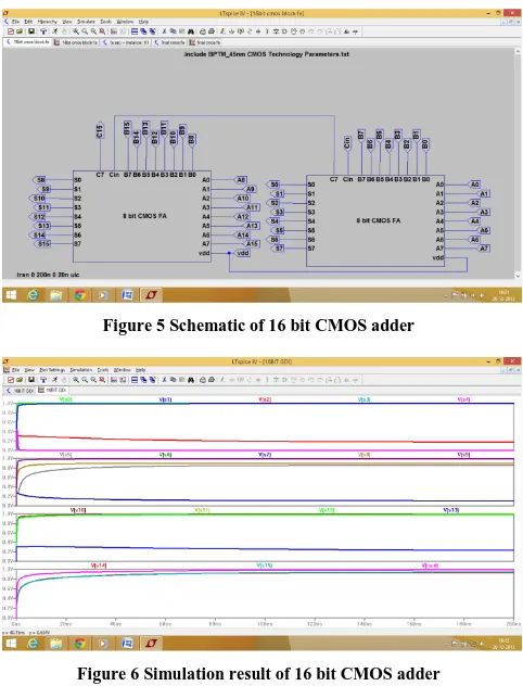
[image:2.612.322.567.341.632.2]All the adders are implemented first with 1bit full adder than 16 bit with help of block of 1 bit full adder. A conventional or static CMOS adder is shown in figure 3 and Simulation result of it shown in figure 4 for 1bit, while 16 bit adder shown in figure 5 and simulation result for all sum output from S0 to S15 and Cout shown in figure 6. As the static or conventional CMOS style is the basic style used in VLSI implementation and basic logic for the development in power reduction technology.
Figure 3 Schematic of CMOS 1 bit adder
[image:2.612.97.238.481.597.2]International Journal of Emerging Technology and Advanced Engineering
Website: www.ijetae.com (ISSN 2250-2459,ISO 9001:2008 Certified Journal, Volume 4, Issue 1, January 2014)
[image:3.612.321.566.95.601.2]218
Figure 5 Schematic of 16 bit CMOS adder
Figure 6 Simulation result of 16 bit CMOS adder
Adiabatic logic, there are various style in Adiabatic technology but we are using 1n 1p Quasi logic which is somewhat similar to the static CMOS logic. The 1n1p quasi adiabatic logic basically, it is similar to conventional CMOS except, it includes a sinusoidal power clock instead of dc power supply. By implementing 1n1p quasi adiabatic logic, it is possible to achieve quasi adiabatic operations with conventional static CMOS gates under one phase driving. If driver is varied sufficiently slowly, dissipation occurs only during charging and discharging of load capacitor [7]. The sources of power dissipation in 1N1P quasi adiabatic logic are threshold voltage of MOSFET and energy dissipated in NMOS and PMOS resistance while charging and discharging of load capacitance. The use of slowly varying power clocks ensures the small energy dissipation across the ON resistance of MOS devices.
Figure 7 Schematic of 1n 1p Quasi 1bit adder
Figure 8 Simulation result of 1n 1p quasi 1 bit adder
[image:3.612.49.290.131.447.2]International Journal of Emerging Technology and Advanced Engineering
Website: www.ijetae.com (ISSN 2250-2459,ISO 9001:2008 Certified Journal, Volume 4, Issue 1, January 2014)
219
Figure 10 Simulation result of 16 bit 1n 1p Quasi adder
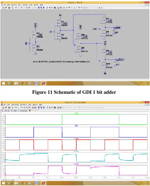
[image:4.612.324.574.116.448.2]As shown in figure 7 1 bit adiabatic 1n 1p quasi adder implemented and simulation result shown in figure 8, while figure 9 shows 16 bit adder with help of the block diagram of 1 bit adder and it's simulation result in figure 10. Similarly the implementation of Gate Diffusion Input logic shown in figure 11, figure 12, figure 13 and figure 14 respectively.
Figure 11 Schematic of GDI 1 bit adder
Figure 12 Simulation result of GDI 1bit adder
Figure 13 Schematic of 16 bit GDI adder
Figure 14 Simulation result of 16 bit GDI adder
IV. COMPARATIVE ANALYSIS OF ADDERS
TABLEI
POWER DISSIPATION OF 1 BIT ADDERS
Load Capa. (fF)
Average Power Dissipation (in uW)
Static CMOS 1n-1p Quasi GDI
10 5.771 3.2006 3.8739
20 6.1796 3.3343 4.3688
30 6.2233 3.512 4.7982
40 6.3251 3.7406 5.1967
50 6.9587 3.9514 5.6084
60 7.0784 4.132 5.9816
70 7.3718 4.3791 6.3424
80 7.6602 4.626 6.6842
90 8.166 4.8833 70533
[image:4.612.49.290.376.675.2]International Journal of Emerging Technology and Advanced Engineering
Website: www.ijetae.com (ISSN 2250-2459,ISO 9001:2008 Certified Journal, Volume 4, Issue 1, January 2014)
220
TABLEII
POWER DELAY PRODUCT OF 1 BIT ADDERS
Load Capa. (fF)
Average Power Dissipation (in pJ)
Static CMOS 1n-1p Quasi GDI
10 1.1542 0.5761 0.7749
20 1.2359 0.6001 0.8737
30 1.2447 0.6321 0.9596
40 1.265 0.6733 1.0393
50 1.3917 0.7112 1.1217
60 1.4157 0.7437 1.1963
70 1.4744 0.7882 1.2685
80 1.532 0.8326 1.3368
90 1.6332 0.8789 1.4107
100 1.6529 0.9222 1.4804
As shown in the table 1 and table 2 will demonstrate the power consumption and integral power delay product of all three adder for 1 bit full adder. we found that an adiabatic logic 1n 1p Quasi has the least power dissipation compared to the GDI and static CMOS logic adder.
REFERENCES
[1] Sauvagya Ranjan Sahoo, Kamala Kanta Mahapatra, "Design of Low Power and High Speed Ripple Carry Adder Using Modified Feedthrough Logic " in 2012 International Conference on Communications, Devices and Intelligent Systems (CODIS) , 978-1-4673-4700-6/12/$3l.00 ©2012 IEEE.
[2] Soolmaz Abbasalizadeh, Behjat Forouzandeh, "Full Adder Design with GDI Cell and Independent Double Gate Transistor " in 20th Iranian Conference on Electrical Engineering, (lCEE2012), May 15-17,2012, Tehran, Iran , 978-1-4673-1148-9/12/$3l.00 ©2012 IEEE. [3] Praveen Saxena, dinesh Chandra and Sampath kumar, Design Of A
1-Bit Full Adder For Low Power Application, in (IJAEST) International Journal Of Advanced Engineering Sciences And Technologies Vol No. 10, Issue No. 1, 019 – 025, 2011.
[4] Y. Sunil Gavaskar Reddy and V.V.G.S.Rajendra Prasad, The Power Comparison Of Cmos And Adiabatic Full Adder Circuits in International Journal of VLSI design & Communication Systems (VLSICS) Vol.2, No.3, September 2011.
[5] Praveen Saxena, dinesh Chandra and Sampath kumar, An Adiabatic Approach For Low Power Full Adder Designa, in International Journal on Computer Science and Engineering (IJCSE) Vol. 3 No. 9 september 2011.
[6] Subodh Wairya, Rajendra Kumar Nagaria and Sudarshan Tiwari, ―Comparative Performance Analysis of XOR/XNOR Function Based High-Speed CMOS Full Adder Circuits For Low Voltage VLSI Design,‖ in International Journal of VLSI design & Communication Systems (VLSICS) Vol.3, No.2, April 2012. [7] A. Kishore Kumar, D. Somasundareswari, V. Duraisamy, T.
Shunbaga Pradeepa, Design of Low Power Full Adder using Asynchronous Adiabatic Logic in European Journal of Scientific Research ISSN 1450-216X Vol.63 No.3 (2011), pp. 358-367. [8] Manoj Kumar, Sandeep K. Arya and Sujata Pandey, Single bit full
adder design using 8 transistors with novel 3 transistors XNOR gate in International Journal of VLSI design & Communication Systems (VLSICS) Vol.2, No.4, December 2011.