International Journal of Emerging Technology and Advanced Engineering
Website: www.ijetae.com (ISSN 2250-2459,ISO 9001:2008 Certified Journal, Volume 5, Issue 3, March 2015)
260
Comparison between Different Control Methods for Switched
Inductor Quasi Z-Source Inverter
Gaurav Sharma
1, Ankita Kosti
21
M-Tech Student, S.R.I.T. Jabalpur (M.P), India
2Assistant Professor, Dept of Electrical Engineering, S.R.I.T. Jabalpur (M.P), India
Abstract— This paper explores Switched Inductor (SL) Quasi Z-source Inverter which has high boost factor and performance when compared to other Z-Source inverters along with three control methods: simple boost, maximum boost and maximum constant boost. The proposed inverter improves the input current, reduces the passive count and also
the reliability. The simulations are done in
MATLAB/Simulink environment by using same input voltage ratio and output load. From different control methods proposed, maximum constant boost provides the highest boost factor as well as reduces passive component requirement along with ripples.
Index terms— Duty Ratio, Inverter, Maximum Constant Boost, Modulation Index.
I. INTRODUCTION
Voltage and current-source inverters [1], [2] are widely used in industries for various purposes like for ac motor drives, distributed power systems, uninterruptible power supplies, hybrid electric vehicles etc. However, these inverters suffer from some major problems such as a voltage source inverter cannot have an ac output voltage higher than dc source voltage . Moreover it can only provide buck dc-ac power conversion. Similarly, a current-source inverter cannot have an ac output voltage lower than dc source voltage and hence can only provide voltage boost
dc-ac power conversion.Apart from the various advantages
reduction in noise , both buck and boost ability it also suffers from disadvantages like input current is discontinuous .To overcome the short comings of classical SI [3] a class of quasi –ZSIs has been proposed [4]-[5] as shown in fig 1.
Fig 1 . Continuous input current q-ZSI
It has the advantages such as reduced passive component ratings and improving the input profiles by providing continuous current .The q ZSI involves lower voltage stress on capacitors and boost factor of classical ZSI and q ZSI can be given the relation:
B = (1)
Where D = (To is the interval of shoot through state
during switching period T)
International Journal of Emerging Technology and Advanced Engineering
Website: www.ijetae.com (ISSN 2250-2459,ISO 9001:2008 Certified Journal, Volume 5, Issue 3, March 2015)
261
[image:2.612.51.279.262.435.2]The technique proposed has advantages like high power quality, high boost factor and power inversion ability. But despite the above advantages startup inrush current problem occurs which causes Z- source inductors and capacitors to resonate and generate the voltage spikes [6]. Hence here is presented SL-qZSI [7] which improves the input current, reliability and passive components. Moreover the shoot through current ,voltage and current stress are lower in proposed SL-qZSI making it applicable in different applications. Fig 2. shows the proposed topology:
Fig 2. SL-qZSI with continuous input current
Hence from all the proposed inverters SL-q ZSI provides the high boost factor as compared to simple ZSI .The maximum constant boost control provides the enhanced voltage boost and reduces the volume and the cost of the inverter. So Maximum Constant Boost control of SL-qZSI inverter has following advantages .
1.Switched inductor and shoot through duty ratio provides boost factor comparatively higher. 2.Less current ripples .
3.Volume and cost of the inverter is reduced.
II. TOPOLOGY ANALYSIS
As seen in fig 2 the proposed inverter consists of three inductors (L1, L2 and L3 ), two capacitors (C1 and C2) and four diodes (Din,D1,D2and D3).The combination of L2-L3-D1-D2-D3 acts as a switched inductor cell. The proposed topology provides inrush current suppression ,however the inductors and capacitors in proposed inverter still resonate. Compared with a conventional q-ZSI the proposed inverter adds only three diodes and one inductor.
A. Operating Principle :
The proposed SL-q ZSI has extra shoot through zero state besides the six traditional active states and two zero states as in classic ZSI. Thus the operating principle is same to classical ZSI. For the purpose of analysis the operating states are classified into shoot -through and non- shoot through states .
1. Nonshoot-Through State : In this state as shown in fig 3 inverter has six active states and two zero states .During this state Din and D1are on while D2and D3 are off. L2 and L3 are connected in series .The capacitors C1 and C2 are
charged ,while the inductors L1, L2 and L3 transfer energy
from dc voltage source to the main circuit .In this state voltages across L2 and L3 are VL2non and VL3non . We obtain
following equations:
VL1 = VC1 - VO (2)
VL2 = VL2_non = VC2-VL3_non (3)
VL3 = VL3non = VC2-VL2non (4)
[image:2.612.327.560.318.547.2]VPN = VC1 + VC2 (5)
Fig 3.Nonshoot-through of SL-qZSI 2. Shoot-Through State: In this state as shown in fig 4. both the upper and lower switches of the same and phase leg are short circuit. During this state , diodes Din and D1are off, while D2and D3 are on .The inductor L2 and L3 are connected in parallel and store energy along with L1. The following equations are obtained : VL1 = -VC2 –VO (6)
International Journal of Emerging Technology and Advanced Engineering
Website: www.ijetae.com (ISSN 2250-2459,ISO 9001:2008 Certified Journal, Volume 5, Issue 3, March 2015)
[image:3.612.325.580.431.622.2]262
Fig 4. Shoot-through of SL-qZSI
III. ANALYSIS OF CONTROL METHODS OF SLQUASI -
Z-SOURCE INVERTER
A. Simple Boost Control:
This control strategy inserts shoot through in all the PWM traditional zero states during one switching period this maintains the six active states unchanged as in the traditional carrier based PWM [7]. Two straight lines are employed to realize the shoot through duty ratio (Do). The first one is equal to the peak value of the three-phase sinusoidal reference voltages while the other one is the negative of the first one. Whenever the triangular carrier signal is higher than the positive straight line or lower than the negative straight line, the inverter will operate in shoot-through. Otherwise it works as a traditional PWM inverter.
B. Maximum Boost Control:
Reducing the voltage stress under a desired voltage gain now becomes important to the control of Z source inverter. As analyzed above, the voltage gain is defined as MB, and the voltage stress across the switches is BV0, therefore, to minimize the voltage stress for any given voltage gain, we have to minimize B and maximize M, with the restriction of that their product is the desired value.
On the other hand, we should maximize B for any given modulation index to achieve the maximum voltage gain [6]. The proposed method is quite similar to the traditional carrier-based PWM control method.
Compared with the simple control method, the voltage stress in the proposed control method is much lower, which means that for given devices, the inverter can be operated to obtain a higher voltage gain.
C. Maximum Constant Boost Control:
In order to reduce the volume and cost, it is important always to keep the shoot- through duty ratio constant. At the same time, a greater voltage boost for any given modulation index is desired to reduce the voltage stress across the switches. The maximum constant boost control method achieves the maximum voltage gain while always keeping the shoot-through duty ratio constant. There are five modulation curves in this control method: three reference signals, Va ,Vb, and Vc, and two shoot-through envelope signals, Vp and Vn.
To summarize, this control method produces the maximum constant boost while minimizing the voltage stress. Table 1 gives the summary of different methods.
Table1:
International Journal of Emerging Technology and Advanced Engineering
Website: www.ijetae.com (ISSN 2250-2459,ISO 9001:2008 Certified Journal, Volume 5, Issue 3, March 2015)
263
IV. SIMULATION AND EXPERIMENTAL VERIFICATION
Parameters used for the simulation of SL- q-ZSI are shown in the Table 2 .
Table.2 . Simulation Parameters
Input DC voltage 48V
Output Line –Line voltage 100 V
L1=L2=L3=L4 10mH
C1=C2 1000mF
Carrier frequency 10KHz
Lf 20mH
Cf 30uF
Resistive Load 1000W
For the analysis of performance of the different control methods on switched inductor z-source inverter, the comparison of the different control methods are performed at the fixed value of modulation index 0 .8, input DC voltage 48 V and output load of 1killowatt. Wave forms are shown in the Figures.
Fig.5. Shoot through states in different control methods
Fig.6.Input Current in different control methods
Fig.7 .Voltage across C1in different methods
International Journal of Emerging Technology and Advanced Engineering
Website: www.ijetae.com (ISSN 2250-2459,ISO 9001:2008 Certified Journal, Volume 5, Issue 3, March 2015)
[image:5.612.52.289.117.296.2]264
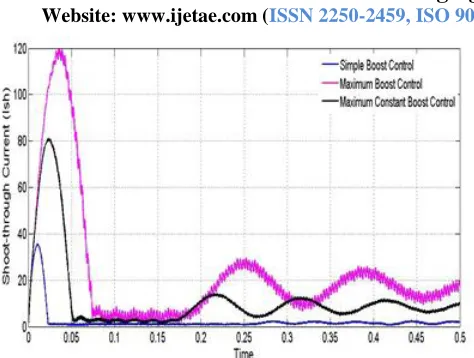
Fig 9. Shoot Through current in different methods
V. CONCLUSION
As we can see from the results obtained that for the same value of modulation index boost factor and gain of maximum boost control is high as compare to others but due to high ripple in shoot-through current and input current, big size of inductor is required and this disadvantage makes maximum constant boost control best method available.
REFERENCES
[1] C. Yang and K. Smedley, “Three –phase boost type grid connected
inverter”, IEEE Trans Power Electro ,vol.23,no.5.pp 2301-2309, Sep 2008.
[2] T. Kerekes , R. Teodorescu and M. Summer , “Evaluation of three phase transformerless Photovoltaic inverter”, IEEE Trans, vol24, no9, pp.2202-2211,Sep 2009.
[3] F.Z Peng , “Z Source Inverter”, IEEE Trans .Ind Application, vol39,
no.2. pp.504-510, April 2003.
[4] J. Anderson and F.Z Peng “Four quasi Z Source inverters” in Proc
.IEEE in Proc. IEEE PESC, 08, Jun .2008,pp. 2743-2749.
[5] M.K. Nguyen, Y.G. Jung and Y.C .Lim, “Single phase ac-ac
converter based on quasi Z source topology” IEEE Trans, Power Electron, vol 25 ,no 8,pp . 2200-2210, Aug 2010 .
[6] W.Qian ,F.Z. Peng and H.Cha „Trans –Z- Source Inverters ‟IEEE
IPEC- Sapporo 2010 , Jun. 2010 pp.1874-1881.
[7] Nguyen, M.-K ; Lim ,Y.-C „Switched Inductor Quasi Zsource