VAX 6000 Model 400 System
Digital Technical Journal
Digital Equipment Corporation
Cover Design
Our cover depicts some of the common equations and terminology used in vector processing, which is one of the featured topics in this issue. The v.-IXl'ector processor extends the VAX 6000 family to address the compul ing need� (if numerically intensiue applications. The VAX 6000 Model •iOO systern is a bright star in Digital's family of midrange multiprocessors and this issue's main product thenU!.
The couer was des(rt,ned by David Comberg and Randy Ziegler of the C01porate Design Group.
Rarhara Lindmark, Associate Ediwr Richard W. Hcane, Managing Editor Circulation
Catherine M. Phillips, Administrator Suzanne ,I. Babineau. Secretary Production
Hden L. l'allcrson. Production Editor Nancr Jones. Typographer
Rebecca A. Barker, Typographer l'ct<:r Woodhury, Illustrator �nd Designer Advisory Board
S:unud H. Fuller. Chairman Robert M. Glorioso John W. McCredie Mahendra R. Patel F (;rant Saviers
Robt:rt K. Spitz
William D. Strecker Victor A. Vyssotsky
The Ui!iila/ Tecbnica/joumal is puhlished quarterly by Digital Equipment Corporation, J46 M:tin Street MLOI-5JB68. Maymrd. Massachusetts 01754-2571. Subscriptions 10 the Journal are S·iO.OO for four issues and must he prepaid in li.S. funds. Univer sity and college professors and Ph. 0. students in the electrical engint:ering and computer science fields receive complimen tarr suhscriptions upon request. Orders. inquiries. and address changes should be sent to The Di!!ita/'lecbnical}oumal at the published-by address. Inquiries on also be sent electronically on NI:ARNET to [email protected]. Single copies and back issues are 3vaibhk for S 16.00 each from Digit:! I Press of Digital Equipmc:nt Corporation, 12 Crosby Drive, Hcdlord. MA 01-_�0- 149.'1. Digital employees may send subscription orders on the ENET 10 RDVAX JOliRNAL or by interoffice mail to mailstop MLO 1- 5/ll68. Orders should include badge number, cost center, site location code and address, and group name. ll s. engineers in Enginen ing and Manufacturing receive complimt:mary subscriptions; enginc:er� in tht:se organizations in countries outside the: lJ.S. should com act the journal office to receive: their complimemary subscriptions. All employees must advise of changes of address. Commt·nts on the content of any paper are wdcomed and may
be sem 10 the editor at the published-b\' or nc:t work address. Copyright' 1990 Digital Equipment Corporation. Copying without fcc is permitJed provided that such copies are made for use in educational institutions by faculty members and are not disJributed for comml'rcial ad,·antage. Abstracting "'ith credit of Digital Equipment Corporation's authorship is permitted.
All rights reserved.
The information in this journal is suhject 10 change without notice and should not be construed as a commitment by Digital Equipment Corporation. Digital Equipmem Corporation assumc:s no responsibility for any errors that may appear in this journal.
ISSN 0898-90 I X
Documentation Number EY-<:1971:-0P
The following are trademarks of Digital Equipment Corpora tion: CJ, OECnet, DECst:uion .'1100, OH:wimlows, Digital, the Digital logo, HSC. MicroVAX, llZ'i'), ThinWire, VAX, VAX-11/780. VAX 6000, VAX 8700, VAX HHOO, VAX 9000, VAXBJ, VAXcluster, VAX FORTRAN, VAXveclOr(J000, V.\1S, !ILTRtX, XMI.
!IN IX is a registered trademark of American Telt:phone &
Telegraph Company.
dbx is a registered trademark of dbx, Inc
I
Contents
9
Foreword Pauline A. NistVAX 6000 Model400 System
11 Vector Processing on the
VAX
vector 6000 Model400Debra L. Slater, David M. Fenwick, D. John Shakshober, and Douglas D. Williams
27
TheVAX
6000 Model400 Scalar Processor ModulePatrick Sullivan, Michael A. Callander, Sr. ,James R. Lundberg, Rebecca L. Stamm, and William). Bowhill
36
An Overview of theVAX
6000 Model400 Chip SetW. Hugh Durdan, William). Bowhiii,John F Brown, William V. Herrick, Richard C. Marcello, Sridhar Samudrala, G. Michael Uhler, and Nicholas Wade
52 VAX
6000 Model400 Physical Technologyjohn T. Bartoszek, Robert). Hannemann, Stephen P. Hansen, Robert]. McCarty, and john C. Sweeney
64
VAX 6000 Model 400 CPU Chip Set Functional Design Verification
Richard E. Calcagni and Will Sherwood73
Test and Qualification of theVAX
6000 Model400 System John W Croll, Larry T. Camilli, and Anthony]. Vaccaro84
Development of the DECstation 3100Thomas C. Furlong, Michael). K . Nielsen, and Neil C. Wilhelm
89
Compiler Optimization in RISC SystemsI
Editor's Introduction
jane
C. Blake EditorThis Spring 1990 issue marks the second issue to be published on the new quarterly schedule of the
Digital Technicaljournal.
This is also the ftrst year that the Journal is available by subscription- a service our readers have asked for and which we are glad to be able to offer.The journal will continue to focus each issue on a product theme. In fact, two products are featured in this issue. The main theme is the latest addition to the V�'l: 6000 family, the Model400. With its multi processing capabilities, this midrange family of systems provides a highly configurable and expand able computing environment. Because the same cabinet, buses, and power systems are used by aU family members, systems can easily be upgraded to achieve higher levels of performance. Papers in this issue describe VAX 6000 Model 400 innovations and additions, including a new vector processor and a higher performance scalar processor module, chip set design and verification, physical technology advances, and system test. The second theme com prises two papers related to Digital's workstation development, specifically the DECstation 3100, and compiler optin1ization in RISC systems.
Opening this issue is a paper on one of Digital's first vector processors. Dave Fenwick, john Shakshober, Debra Slater, and Doug Williams review the design alternatives for the VAXvector 6000 Model 400 processor and describe its function units. They then give examples of how the units combine to deliver high performance for computa tionally i ntensive applications.
The Model 400 also has a new scalar processor, with nearly twice the performance of its prede cessor, the Model 300. In their paper, Pat Sullivan, Mike Callander, Jim Lundberg, Rebecca Stamm, and
2
Bill Bowhill discuss the module design and give particulars on how difficult signal integrity prob lems were resolved.
The five system chips that reside on the module are the topic of our next paper by Hugh Durdan, Bill Bowhill, John Brown, Bill Hl:rrick, Rich Marcello, Sri Samudrala, Mike Uhler, and Nick Wade. From their d iscussions of the chip designs, we learn how the best features of the VAX 8700 ECL-based, pipelined system and of previous VLSJ designs were incorporated i n the chip set, which achieves a cycle tinle of 28 nanoseconds.
This fast cycle time was one of several require ments that drove a significant design effort for the physical technology. Joh n B a rtoszek, Rob Hannemann , Steve Hansen, Bob McCarty, and John Sweeney describe the technological advances achieved in a number of areas, including tape automated bonding, semicustomized ceramic single-chip package design, and testability.
The two papers that close this collection of papers on the VAX 6000 Model 400 address chip design verification and system test. Rick Calcagni and Will Sherwood explain the engineers' multipronged approach to design verification, an approach neces sitated by the complexity of the chip set. Then, John Croll , larry Camilli, and Tony Vaccaro present a paper on the methods and tools designed to com pletely test the i nteraction of VAX 6000 Model 400 system's hardware and software.
In the last rwo papers, the topic turns to work stations. Tom F u rlong, Mike N ielsen, and Neil Wi.lhelm provide an overview of the successful project undertaken to bui.ld a fast, competitively priced, RJSC-based, ULTRIX workstation, called the DECstation 3 100. The Journal is fortunate also to have a related paper on compiler optimization in RISC systems by Larry Weber, vice president, MIPS Systems, I nc. MIPS Systems built the RJSC chip set incorporated in the DECstation 3100 workstation.
Biographies
John T. Bartoszek john Bartoszek currently manages the Physical Technology Group within the SDE that is responsible for physical technology applications and product designs. John previously managed the PTG physical technology pro gram that spawned the physical technology used on the VAX 6000 Model 400 CPU module. He joined Digital in 1981 and has a B.S. in nuclear engineering from Lowell Technological Institute. He holds two patents for thermal control devices. john has authored several papers on spacecraft thermal control, solar energy, and
electronics cooling and interconnect technologies.
William). Bowhill As a principal engineer with the Semiconductor Engineer ing Group, William Bowhill is project leader for an engineering team that is designing an execution unit section of a large CMOS-based microprocessor. He has applied for two patents for his design work on the vector interface and backup control chip on the VAX 6000 Model 400 system. Bill also holds a patent for his work in relation to the Model 400's floating poinr accelerator chip. He joined Digital in 1985. Bill was educated in Great Britain and received a B.Eng. (honors) in electronic engineering from Liverpool University.
John F. Brown After receiving an M. S.E.E. from Cornell University in 1980, John Brown joined Digital's engineering staff. At present, he is a principal engi neer and design team manager for the instruction decode section of the next generation CMOS-based VAX microprocessor. John's previous responsibilities include technical contributions to both the VAX 6000 Model 400 and the Model 200 chip sets. He was also the hardware engineer for the extended floating point data type enhancement to the VAX-11/780 system. John currently holds one patent, has two patent applications pending, and has authored technical papers for several publications.
Richard E. Calcagni A member of the Semiconductor Engineering Group's VLSI microprocessor verification group, Richard Calcagni has contributed to the design of several VLSI microprocessors in the areas of microcode, verification, and prototype system debugging. He has published several papers on CPU design, modeling, and verification. Prior to his work with microprocessors, he worked on module test process development for Digital's Customer Services Manufacturing organization. Before joining Digital in 1979, Rick worked for Burroughs Corporation. He received a B.S. (1976) in electrical engineering from the University of Rhode Island.
Michael A. Callander, Sr. Michael Callander is a principal engineer in Digital's Semiconductor Engineering Group. At present, he is responsible for the archi tecture of a future VAX CPU module. Mike led the VAX 6000 Model 400 system's REXMI chip set design project. His previous experience with Digital includes the design and verification of the CPU module for the VAX 8200 system and the VAX 8300 system. Mike received his B.S.E.E. degree from the University of Massachusetts in 1982. He joined Digital upon graduation.
I
4
Larry T. Camilli Since joining Digital in 1979, Larry Camilli has been a member of several product development projects. He is currently a software cnginL"ering supervisor and project leader for the architecture verification software development project, which focuses on the development and maintenance of test software for current and future architectures. Larry's previous responsi bilities include the development of components for a microcode compiler, and a software trace and analysis package. He holds a B.S.E.E. from Clarkson University and is a student in the M.S.C .S. degree program at Worcester Poly technical Institute.
john Croll John Croll is a principal software engineer in the Midrange Systems Engineering Group. In this position, he is responsible for developing systems test tools for a future hardware product. John was a team leader in tht: Systems Integration Group for the VAX 6000 Model 400 system. He was also a project leader for the development of the VAX 6000 Model 400 console software. John joined Digital in 1978, and his previous responsibilities include the development of device drivers and other system software. He received a B.S. E. E. ( 1978) from Drexel University and is a member of IEEE and ACM .
W. Hugh Durdan A graduate of the Rensselaer Polytechnical Institute, Hugh Durdan is a consulting engineer in the Semiconductor Engineering Group. In this position, his major responsibility is management of chip development. Hugh became involved in the VAX 6000 Model 400's chip design at its earliest begin nings in 1984 . He led the behavioral modeling effort and the cache controller chip design project. He also managed the development of the custom chip set for the VAX vector procL"ssor and aFChitected and specified the vector interface bus. Hugh joined Digital in 19HO and worked on the chip design of the VAX 8200 processor.
David M . Fenwick The architect of the VAX vector 6000 Model 400 processor, David Fenwick joined Digital's United Kingdom office in 1980 and transferred to the Cnited StatL"s in 1985. He is a principal engineer for the Low End Midrange Systems Group. His previous experience with Digital includes field service regional support in the 'nited Kingdom and project leadership for the DMB32 communications controller for the European engineering office. He also worked on the VAXBI and XMI programs in the United States. Dave received a B.Sc. (Honors) from Loughborough University of Technology in England.
Robert J. Hannemann
Robert Hannemann is group manager of the
SCITDesign and Engineering Physical Technology Group. His group is responsible
for the delivery of
ICpackaging, module, physical design and test technology
for Digital's microprocessor-based systems. A senior consultant engineer, Rob
joined Digital in 1978. His prior experience includes positions at Bell Telephone
Laboratories and the University of Maryland, where he was a member of the
faculty. Rob holds the Sc.D. degree in mechanical engineering from MIT. He also
holds two patents and has published several papers on heat transfer engineering
and electronics packaging.
Stephen P. Hansen
Senior Manager Stephen Hansen manages the SDE/PTG
Technical Office. In this position, he coordinates programs related to cost
effective packaging for future CMOS-based products, defines technical solutions
for the next generation of semiconductor packaging, and provides technical
coordination for external packaging and interconnect-related activities. In his
twelve years with Digital, Steve has developed several packages and assembly
processes for internally manufactured CMOS products, including the tape
automated bonding process. He holds two patents in the areas of tape-automated
bonding and packaging.
William V. Herrick
Senior Consultant Engineer William Herrick is currently
managing a new generation
VAXchip design project in the Semiconductor
Engineering Group. He joined Digital in 1977 and has been a member of many
ZMOS- and CMOS-based product development projects, including the PDP-11123
system and the
VAX8200 system. Before coming to Digital, Bill worked for
Raytheon and
GTESylvania. He has coauthored several papers on solid-state
physics and
MOSchip design. Bill received a
B.S.E.E. ( 1969, magna cum laude)from Tufts University, and an S.M.E.E.
(1971) and
E.E.(1971) from MIT and is a
member of Tau Beta Pi, Eta Kappa Nu, and Sigma Xi.
James R. Lundberg
James Lundberg joined Digital in 1985. Initially, he was a
product engineer with the MOS Product Engineering Group and worked on
many projects, including
BIIC and CQBIC. Jim is currently a senior engineer inDigital's Semiconductor Engineering Group. He was responsible for the signal
integrity on the VAX 6000 Model 400 system and is now working on the signal
integrity for an advanced CMOS CPU chip set and module. Before coming to
Digital, Jim operated his own business. He is a member of Tau Beta Pi and Phi
Kappa Phi. He received a B.S.E.E. (1985, honors) from the University of Illinois.
Richard C. Marcello
A contributor to the design of the VAX 6000 Model 400
system, Richard Marcello is currently an engineering manager for a new
generation VAX chip design project. Rich was involved with reliability analysis of
semiconductor devices before moving into design five years ago. He worked for
Fairchild Semiconductor before joining Digital in 1981 . Rich coauthored the
paper "System, Process and Design Implications of a Reduced Supply Voltage
Microprocessor," which he recently presented at the
ISSCC .He received
B.B.A.and
B.S.E.E. (1980) degrees from the University of Notre Dame and a M.S.C.S.(1985) degree from Boston University.
I
6
Robert j. McCarty
Since joining Digital in 1982 , Robert McCarty has hn:n
involved in several major product development efforts. He managed the
VAX 6000 Model 400 system's physical design project and M31 console and
instrumentation module development, and led the PDP-11184 system engineer
ing project. Before coming to Digital, Bob worked for AM International as the
project leader for a laser-based document printer that was part of a document
communication system. He holds a B.S. in electrical engineering from the
University of Michigan and an M.B.A. in marketing from the University of
Chicago. He is a member of Tau Beta Pi and Eta Kappa Nu.
Michael j. K. Nielsen
A consultant engineer in the Workstation Systems
Engineering Group, Michael Nielsen is presently completing his responsibilities
as architect and chief designer of the DECstation 5000 Model 200 workstation
base platform. Mike joined Digital in 1 984. Among the many projects he has
worked on since that time are the DECstation 3100 workstation, for which he
was the architect and chief designer, and the VAXstation 3520/3540, for which he
was a member of the architecture and design team. Mike holds B.S.E.E., M.S.E.E. ,
and Ph . D.E.E. degrees from Stanford University. He is a member of Tau Beta Pi
and Phi Beta Kappa.
Sridhar Samudrala
Currently acting as project leader for a floating point
unit, Sridhar Samudrala is a principal hardware engineer in the Semiconductor
Engineering Group. Sri joined Digital in 1977. Since that time, he has worked on
testing and diagnostics, as well as the VAX 8200 system microcode, and floating
point architecture and design. He holds two patents for his work in floating
point design. Sri has an M.Sc. (Technology) from Andhra University in India and
an M.S. E. E. from the University of Wisconsin.
D. john Shaks hober
John Shakshober is a senior hardware engineer in the
Low End Midrange Systems Group. Previously involved in the hardware design
of M31, a VAX parallel processor, John is now a member of the
VAX6000
Model 400 hardware group, where his particular focus is vector processor
design. He joined Digital in 1984 after receiving a B.S. in computer engineering
from the Rochester Institute of Technology. John received a M.S.E.E. from
Cornell University in 1988. He is a member of IEEE and Tau Beta Pi. John's latest
published technical paper, "Parallel Algorithms for Super Performance," was
presented at SuperComputing 89.
Debra L. Slater
In her position as principal software engineer, Debra Slater
leads a group that provides performance modeling and analysis support to hard
ware development teams. She and her group were integral members of the
VAXvector 6000 Model400 vector processor design team. Prior to joining Digital
in 1987, Debra worked for the Montreal Engineering Company, initially as a pro
grammer/analyst and later as an independent consultant. She received a B.Sc. in
mathematics and computer science in 1980 from Bishop's University in Quebec.
In 1981, Debra received a master's degree in applied mathematics from the
University of Waterloo in Ontario .
Rebecca L. Stanun
Rebecca St
ammis a principal hardware engineer in the
Semiconductor Engineering Group. She is currently leading the design of the
backup cache, bus interface, and pin bus for a new
VAXCPU chip. Rebecca was
the architect of the backup cache controller chip for the
VAX6000 Model 400
system. She has also worked on design and verification of a RISC microprocessor.
Rebecca joined Digital in 1983. She is a member of Eta Kappa Nu and
I EEE,holds
one patent, and has coauthored several technical papers for the ISSCC. She
received a
B.A.(1979) in history from Swarthmore College and a
B.S.E.E.( 1983)
from
M IT.Patrick Sullivan
The project leader for the
VAX6000 Model400 CPU module
development, Patrick Sullivan is a hardware consultant engineer in Digital's
Semiconductor Engineering Group. Pat is now managing a new CPU module
development project. Before his work on the
VAX6000 Model 400, he led the
group effort that brought
MCAemitter-coupled logic (ECL) into the corporation.
He is also responsible for the development of a number of Digital's main memory
products and participated in the development of several 36-bit CPUs. Pat holds a
patent for a memory controller interface. He received his
B.S.and
M.S.degrees
from Northeastern University.
john C. Sweeney
Currently a principal engineer, John Sweeney is working on
the testability and test process development for a future Digital product. His
previous experience includes being part of the test process development for the
VAX8600 and
VAX8800 systems . .John was an application engineer for
GENRADbefore joining Digital in 1981. He has authored several papers on boundary scan
and fault isolation, and has one patent pending in relation to the
VAX6000 Model
400 system's test structures. john received a
B. S. E. E.(1980) from Rensselaer Poly
technical Institute and has taken graduate courses at Northeastern University.
G. Michael Uhler
G. M ichael Uhler is a consulting engineer in the Semi
conductor Engineering Group, where he is currently leading the architectural
definition for a new CPU. As the CPU architect for the
VAX6000 Model 400
system, M ike was responsible for the CPU architecture, performance evaluation,
and CPU microcode. Since joining Digital in 1978, he has also worked on the
development of symmetric multiprocessing in the TOPS-10 operating system, and
on the microcode and hardware development for PDP-10 CPUs. Mike received a
B.S.E.E.(1975) and
M.S.C.S.( 1977) from the University of Arizona and is a member
of
I EEE, ACM,Tau Beta Pi, and Phi Kappa Phi.
I
8
Anthony J. Vaccaro
A senior engineer in the Midrange Systems Evaluation
Group, Anthony Vaccaro is at present responsible for several evaluation projects.
These projects include the FV64A VAX 6000 Model 400 vector processor and
KDM70 mass storage controller. Tony joined Digital in 1976 as a field engineer.
Some of his earlier project responsibilities include product evaluations for the
CIBCA-B VAXcluster Cl adapter and KA825 VAX processor. He was also a member
of the team that developed a certification process for new VAXBI adapters. Tony
holds a B.S. (1975, cum laude) from Suffolk University and is studying for an
M.S.C.S. at Rivier College.
Nicholas Wade
The implementation of the backup cache control for the next
generation VAX CPU chip is being led by Nicholas Wade. Nick is a senior engineer
in the Semiconductor Engineering Group. He joined Digital in 1986 and has
worked on several projects, including the VAX 6000 Model 400 chip set. He
performed the engineering evaluation and debugging for the system support
chip on the VAX 3500 and VAX 6000 Model 200 systems. Nick was also a member
of the behavioral design and implementation feasibility project for a CPU-XMI
interface. He holds B.S. (1985) and M.S. (1986) degrees from Cornell University
and is a member of
IEEE.Larry B. �ber
As vice president of software development for MIPS Computer
Systems, Inc., Larry Weber is responsible for the development, quality assurance,
and integration of all systems software products. Larry is one of M IPS first
employees, having joined the company in 1984. Prior to joining MIPS, he worked
for Dialogic Systems and for IBM. Larry helped develop a PASCAL compiler for
both the IBM mainframe and IBM RISC project. He has authored and coauthored a
number of articles on compilers and languages. Larry holds a B.S. in mathematics
from the State University of New York and an M.S. in computer science from the
University of Colorado.
Neil C. Wilhelm
Neil Wilhelm, a senior consultant engineer, is responsible for
the development and maintenance of the Workstation Systems Engineering
Group's CAD system and the design engineering of a low-cost workstation. Neil
also designed Digital's first RISC-based system. Neil brought an extensive tech
nical background to Digital when he joined the company in 1982. He has worked
for Hewlett-Packard and Xerox Corporation, founded Ridge Computers, and
taught at the University of Rochester. Neil holds a B.S. (1970) in engineering from
Harvey Mudd College, and an M.S. (1971) and a
Ph . D.
(1973) in electrical engi
neering from Stanford University.
I
Foreword
Pauline A. Nist
Group Engineering Manager Midrange Systems Business
Because microprocessor-based computer systems are complex, the work to design and architect cus tom chips must be initiated long before module and systems work begins.
Looking back at recent history, Digital intro· duced the VAX 6000 family of computers in April 1988 with the Model 200 series, which utilized the ftrst generation of the CMOS-based VAX micropro cessor. The Model 200 was fabricated in Digital's CMOS-1 (complementary metal oxide semiconduc tor) process. A single-processor Model 210 pro vided 2.8 times the performance of a VAX-11/780 system. One to four processor configurations pro vided up to a total of
1 1 times the performance of a
VAX-11/780 system. (Papers discuss these chips and systems in the August 1988 issue of this journal.)In January 1989, Digital introduced the second generation of the VAX 6000 family, the Model 300 series. The Model 300 increased single-processor performance from 2.8 to 3.8 times the VAX-11/780 system and total performance for a six-processor system to 22 times the VAX-11/780 system. The 30 percent increase in single-processor perfor mance was made possible by a direct shrink of the die from Digital's 2.0 micron CMOS-1 process to Digital's
1.5
micron CMOS-2 process. The new pro cess supported a 25 percent reduction in lateral and key vertical dimensions and a 78 percent improve ment in circuit density. Together, these changes improved chip performance by approximately 30 percent.However, a simple shrink of the existing die did not permit full exploitation of the new circuit den sity. Newly architected and designed parts had to be tailored to take full advantage of the density and speed available with the CMOS-2 process.
The VAX 6000 Model 400 series was formally introduced in July 1989, a mere SLX months after the
Model 300 was introduced. The Model 400 utilized this newly architected chip set to provide single processor performance of 7 times that of the VAX-11/780 system and up to 36 times the VAX-11/780 system for six-processor systems. The performance of the Model 400 was over twice the single-processor performance and more than three times the multiprocessor performance of the Model 200 series, which had been announced only a short
15
months earlier.To support such aggressive product introduction cycles, advanced development work on the new generation of CMOS-2 chips began in mid-1984, within months of the start of the CMOS-I designs. Actual design work began approximately a year later. During this period, Digital made a major deci sion to formally extend the VAX architecture to incorporate full support for vector processing into the base instruction set for aU future VAX proces sors. To provide this support, the chip designs already under way had to be modified to incorpo rate the new instructions.
The scalar chip set developed consists of ftve cus tom VLSI parts. They are the
CPU chip, the floating
point accelerator chip, the vector/cache controller chip, the system support chip, and the clock chip. The development of the custom chips required a team of over 40 people, including logic, circuit, and layout designers, and verification engineers. The scalarCPU
module design, standard cell interface design, and associated verification team comprised an additional eight engineers. Additionally, the new vector coprocessor module required three new cus tom parts, a new gate array, and a separate module design effort.Since the direct shrink of die from the CMOS-1 to CMOS-2 process would account for only a 30 per cent performance increase, the processor architec ture had to be substantially changed to achieve more aggressive performance. Early in the project the chip design team established a clear goal to meet or exceed the performance of the VAX 8700 proces sor, which has a performance of five times that of the VAX-11/780 system. Some of the architectural changes included the following:
• A more pipelined architecture, specifically, a six level pipelined engine built around three auto nomous pipes
• A 64-bit wide data bus with 27 separate address
lines versus a 32-bit multiplexed data/address bus used for the CMOS-I chip
I
•
Support for decode of the new VAX vector
instructions and transfer of instruction operand
information to the vector interface bus and onto
the vector coprocessor module
•
A 2 kilobyte (K B) primary on-chip cache with
single-cycle access supported by a 128KB off
chip secondary cache
•
A 16-byte instruction prefetch queue
•
Two quadword write buffers in the bus interface
unit
Experience with the CMOS- I chip showed that
the fabrication line was capable of producing a dis
tribution of die across a performance range of 80 to
100 nanoseconds (ns). As a result, whereas all
CMOS-2 new designs supported the target of a 40 ns
CPU cycle time, it was an explicit goal to support
devices as fast as 28 ns, should chip yields produce
sufficient quantities of faster parts. The yields at
28 ns actually exceeded predictions and permitted
faster parts to be used in all products produced.
First passes of all scalar CPU chips were available
in April 1988. These chips could successfully boot
both the VMS and ULTRIX operating systems. This
success was due in large part to the aggressive use of
computer-aided design (CAD) techniques. Func
tional design verification efforts alone represented
25 person-years of work on the scalar chip set. An
additional 39 person-years were necessary to com
plete the scalar CPU module and the vector copro
cessor verification efforts.
The power-on of first-pass parts represented a
significant accomplishment to those who worked
on the chips and the module. However, much
"behind the scenes" work was necessary to achieve
this milestone. The success in this area represents
the culmination of work across a number of disci
plines. Besides the semiconductor devices, a new
224-lead multilayer ceramic package was devel
oped. New techniques, including tape-automated
bonding (TAB), were explored to attach the die to
the package, and new specifications were necessary
for the actual printed wire board material and board
layup. Finally, new manufacturing processes were
necessary to permit surface-mount assembly and
test of these devices on both sides of the module.
Although initializing the operating system on the
ftrst CPU modules marks a key deliverable for the
chip and board designers, it is only a starting point
for the systems activity that is necessary to fully test
and qualify a new product prior to the start of
high-10
volume manufacturing. It is often difficult to under
stand the time lag between the availability of the
first prototype unit running the operating system
and a product that can be shipped to the customer.
However, a substantial amount of work must be
done between these two events. As the formal qual
ification process for new semiconductor devices
begins, a parallel effort is undertaken to build a large
number of early systems. These systems are used to
identify any problems that may occur when the
pieces of the system are assembled into configura
tions typical of those used by actual customers.
Testing is divided across several aspects, including
actual beta test of prototype un.its at customer sites,
formal testing by any required government agencies
(e.g., FCC , Ul, V DE), systems design verification
tests, and architectural testing that ensures that the
new system complies with the formal VAX architec
ture standards. Once the majority of testing is in
process and the required interim milestones have
been met, manufacturing begins turning the assem
bled inventory into fin.ished products to support
volume availability of the system.
When a series of systems such as the VAX 6000
family has established a history in the market, it
becomes increasingly important to ensure that the
announcement of the latest family member coin
cides with manufacturing's ability to quickly deliver
a high volume of product on a worldwide basis. If
manufacturing cannot do so, a demand will have
been created that cannot be filled. Revenue and
sales are lost. The full payback from the many per
son-years of design, simulation, design verification,
and systems test is only finally realized when vol
ume manufacturing has begun.
The papers in this issue of the journal will
provide insight not only into how microprocessors
and systems are designed and architected, but also
into the multidisciplinary efforts necessary to bring
a successful product to market. The design of one of
the first VAX vector coprocessors is also reviewed.
This review offers a summary of how new architec
tural issues are resolved and how design trade-offs
are made.
Debra L. Slater David M. Fenwick D. john Shakshober Douglas D. Williams
Vector Processing on the
VAXvector 6000 Model400
The VAX vector 6000 Model 400 processor extends the VAX 6000 family of midrange CMOS-based multiprocessors to address the computing needs of numerically inten sive applications. The three function units of the vector processor combine to form an overall vector pipeline that operates at speeds of up to 90 MFLOPs for single-precision calculations and 45 MFLOPs for double-precision calculations. The processor's per formance can also be enhanced by taking advantage of overlapping and out-of order instruction execution, as well as chaining. Further, applications can be tuned to the VAX vector 6000 hardware through algorithm optimizations in areas such as equation solvers and signal processing routines to achieve optimal performance. Using the VAX vector 6000 Model 400 system, performance increases ranging from 3 to 35 times that of the VAX 6000 Model400 scalar system have been realized.
Vector processing has significantly evolved over t he
past t wo decades. In the late 1960s and early 1970s,
it was pioneered as a way to increase scient ific
applicat io n computer performance over t hat
achieved by more traditional scalar computers.
However, t he technology was limited to an elite
few who could afford mult im ill ion-dollar super
computer systems and who were w illing to sig
nificantly re-engineer software applicat ions.
I n the early
1 980s, more sophisticated
vectorizing compil er technology was developed.
This technology allowed users to effectively pro
gram in high-level languages , such as
FORTRAN,
rather than to manually vectorize using low-level
assembly language. During t his period , t here
were also significant developments in computer
algorithms t hat were better matched to t he paral
lel ism available in vector hardware.
Over t he past few years, a new breed of vector
processor, t he mini-supercomputer, has emerged.
This class of machine includes many of t he perfor
mance features of traditional supercomputers, but
at costs more commonJy associated wit h super
minicomputers. Because vector processing is now a
mainstream sty le of comput ing t hat is applicable to
a wide range of uses, the
VAXarchitecture was
recent ly extended to include vector operations.
Furt her, the
VAXproduct line has been expanded t o
include vector processing in both t he
VAX6000
midrange systems fami ly and t he
VAX9000 main
frame family of systems.l
Digital Tecbnicaljournal Vol. 2 No. 2, Spring 1990
VAX Vector Processing Overview
The extension of t he
VAXarchitecture to include
vector processing features was done in a manner
that permitted a wide range of possible implemen
tations2 The extension also allowed exist ing
VAXprocessors to execute code utilizing t he new vector
instructions under software emulation.
The vector extensions to the
VAXarchitecture
include:
•
The addition of 1 6 vector registers, each contain
ing 64 64-bit elements
•
A set of load/store instructions used to move up
to 64 elements of a vector register to and from
memory
•
A set of vector register-to-register arithmetic and
logical instruct ions, operating on up to 64 ele
ments at a t ime
•
A
set of instructions for sy nch ronization
bet ween scalar and vector processing
subsystems
C on ceptually , the implementat ion of vector
instructions w it hi n the
VAXfamily of processors is
similar to t hat of float i ng point inst ructions. To
implement floating point arit hmet ic, some systems
use dedicated floating point hardware, some sys
tems use microcode, and others emulate fl oat ing
point in macrocode. In vector processing, vector
instructions differ from float ing point instructions
in that they are designed to be executed in a semi
autonomous manner with scalar instructions. Thus,
vecror instmctions can be executed in parallel with
scalar instructions or in parallel with other vector
instructions. Although the scalar and vector units
operate somewhat independently, tht: units art:
closely coupled to ensure that memory manage
ment exceptions are precisely reported. Special
operations ensure floating point exceptions and
coherence between vector and scalar memory ref
erences are synchronized.
From a vector perspt:ctive, a typical VAX vector
implementation can bt: reduced to five hasic units.
The latter four units arc collectively rderred to as a
vector processor or vector unit. The hasic units are:
•
A scalar processor that executes scalar instruc
tions, decodes vector ·instructions, which may
contain multiple internal function units
•
A vector instruction-sequencing control and reg
ister scoreboard
•
A vector register file
•
An arithmetic pipeline or pipelines that consist
of one or more arithmetic/logic units
•
A load/store unit for memory references
The vector control and scoreboard logic accepts
instructions and operands from the scalar processor
ami dispatches them to the individual function units
within the processor. It also reports exceptions and
interrupts to the scalar processor. Since multiple
vector instructions can be executt:d in parallel , the
unit may contain scoreboard logic ro identify and
manage resource conflicts between instructions.
The vector register file contains the 16 vector reg
isters, each of which consists of 64 64-bit elements.
The register file has multiple ports that permit loads
or stores to operate while operands are sent to the
arithmetic pipes and results are received .
The vector arithmetic/logic pipelines implement
all the integer, logical, and floating point instruc
tions. These pipelines may be composed of separate
pipelined add, multiply, and logical units. Or, they
may be composed of multiple pipes that operate in
parallel, with each pipe consisting of a pipelined
add/multiply/logic unit.
The load/store unit is responsibk for memory
references. It generates the required virtual
addresses (VA), performs translation from virtual
to physical addresses, and loads or stores the data
to or from the register files to memory . The load/
1 2
store unit controls a cache memory and contains a
virtual-to-physical address translation buffer
(TB).Depending on the design of the scalar and vector
units, then: are two ways to implement the design
memory interface for the scalar and vector
processors:
•
A combined scal
.
ar and vector processor that
shares a common cache, address translation
logic, and path to memory subsystem
•
Separate scalar and vector units with separate
caches and address translation buffers
Both of these approaches have their relative
merits and disadvantages. When significant data
sharing between scalar and vector units exists, the
combined approach provides more favorable cache
performance because the common cache is updated
on both scalar and vector references. Separate
caches may result in additional cache misses as
data is "sloshed" between scalar and vector caches.
For limited data-sharing instances, the separate
approach may offer more favorable cache perfor
mance. In a combined cache, vector references can
displace needed scalar data and vice versa. This
problem does not arise with separate caches
because the scalar and vector data each has a
dedicated cache. The separate cache approach also
allows scalar and vector cache operations to occur
in parallel.
In implementing a vector processor, the selection
between the above alternatives is often driven
more by technology constraints than issues of archi
tectural elegance. The VAX 9000 system, which is
implemented in emitter-coupled logic (EC L), chose
the combined approach. This approach supported
sharing costly cache RAMS and a common path
to memory. T he VAXvector 6000, which is imple
mented in complementary metal oxide semi
conductor (CMOS) technology, chose the separate
approach for two reasons. First, module space and
package pin count constraints made it difficult to
implement both scalar and vector functions on a
single module. Second, the cost penalties for sepa
rate scalar and vector cache
RAMSand separate
paths to memory were not prohibitive.
VAX 6000 Vector Processor
Description
System Block Diagram
The system block diagram for a vector-capable
VAX 6000 Model 400 machine is shown in Figure 1 .
Vector Processing on the VAX vector 6000 Mode/ 400
SCALAR
I-
VECTOR SCALARI--
VECTORPROCESSOR PROCESSOR PROCESSOR PROCESSOR
I
I
I
...XMI SYSTEM B U S
I
1
I
32MB
l···
32MB Bl. . . D I S K
I
M E MORY M E MORY PORT CONTROL
( U P TO 256MB OR 8 MODULES)
I
CABLEf--
RA 7 0 STRIPESETETH E R N E T VAXBI
BI PORT
D E B N I ESE20
L..
SOLID- STATE DISKRAXX
DISKS KDB
1--Figure 1 VAXvector 6000 Mode/ 400 System Block Diagram
with Dual Scalar and Vector Processors
The vector processor occupies a slot adjacent to the scalar processor, and both are interconnected by a short interface cable. The vectOr processor receives all instructions from and returns status tO the scalar processor across this cable. For memory references, the vectOr processor has its own independent path to main memory . The VAX 6000 Model 400 system supports configurations of up to six scalar proces sors. However, vectOr systems have additional configuration constraints because of the increased memory bandwidth and XMI slot requirements of the scalar/vectOr processor. The VAXvector 6000 Model 4 00 system supports configurations of single or dual scalar/vector processors. or configurations of one scalar/vectOr processor and up tO three addi tional scalar processors. To satisfy memory band width requirements, VAXvectar 6000 systems with a single scalar/vector processor require at least two memory controllers. Dual scalar/vector systems or single scalar/vector systems with additional scalar processors require at least four memory controllers.
VAX 6000 Mode/ 400 Vector Processor
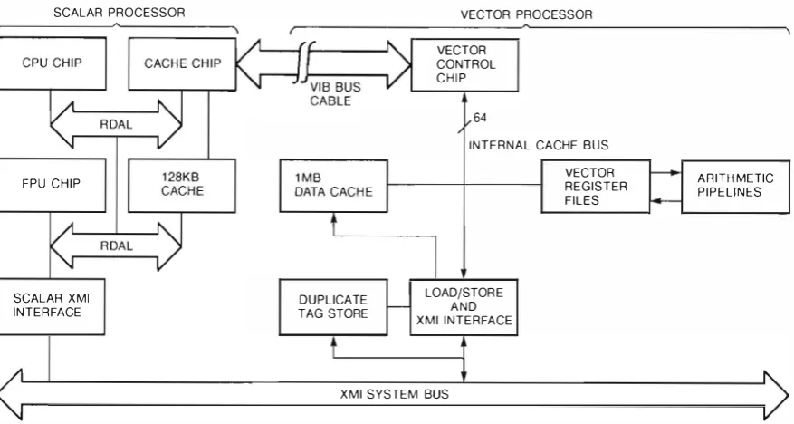
The block diagram for the vector processor is shown in Figure 2. The machine is divided into three separate function u nits that can operate in combination or independently:• A vector controller, implemented as a single chip
• Arithmetic pipelines implemented by four pairs of chips , i . e . , register file and vector data path
Digital Tecbnicaljournal Vol. 2 No. 2, !>/JI"ing 1990
• A load/store unit, implemented by one chip,
which also controls a 1 megabyte (MB) cache
Vector Control Chip
When the scalar processor encounters a vector opcode, it parses and fetches the operands. The opcode and all its operands are dispatched through the instruction bus to the vector processor. For arithmetic instructions, the scalar processor will proceed to decode the next opcode in the instruction stream. However, for load and store instructions, the scalar processor is stalled until all address translations are completed. Stalling guaran tees that any memory management violations are synchronous and that the scalar processor can restart the faulting instruction correctly. Within the vector unit the vector control chip is responsible for all scalar vector communication. When instruc tions are received by the vector controller chip, the vector controller buffers the instructions and controls instructions issuing to the other function units within the vector processor.
An important aspect of the vector control chip is the register scoreboard logic, which identifies potential register conflicts when vector instructions are executed in parallel. By maintaining accurate register usage data, the vector control chip can optimize parallelism with the vector processor. Optimal performance is achieved by executing arithmetic operations in parallel with load and store operations, chaining the results of arithmetic
SCALAR PROCESSOR
FPU C H I P
SCALAR XMI INTERFACE
DUPLICATE TAG STORE
VECTOR PROCESSOR
VECTOR CONTROL C H I P
64
INTERNAL CACHE B U S
LOAD/STOR E A N D X M I INTERFACE
VECTOR REGISTER FILES
A R I T H METIC P I P E L I N ES
[image:16.593.96.535.97.331.2]X M I SYSTEM BUS
Figure 2
VAX vector 6000 Mode/ 400 Scalar/Vector Processor Block Diagram
tions into store operations, and even dynamically re-ordering the execution of arithmetic instructions relative to load and store instructions to improve parallelism.
The vector control chip sends aU error status and machine checks to the scalar processor. When an error is encountered, the control chip attempts to retry the failing transaction. If the retry is suc cessful , a soft error interrupt is sent to the scalar processor. If the retry fails, either a hard error interrupt or a machine check is sent to the scalar processor. Read operations that fail result in machine checks. Write operations that fail result in hard error i nterrupts.
Although not part of the overall control function, the vector control chip also contains logic to imple ment the IOTA instruction. The IOTA instruction builds a set of offsets in a vector register. This func tion did not fit conveniently i n any other vector function. The control chip was selected because it had the space available to contain the function.
Vector Register File and Arithmetic
Pipeline
The VA.Xvector 6000 processor's arithmetic pipe l ine is organized as four pipes. Each pipe consists of a quarter of the register file (every fourth element of the vector registers), and an associated arithmetic/ logic unit. Each i nd iv idual pipeline can retire one single-precision calculation every cycle or one
1 4
double-precision calculation every two cycles. The four pipes collectively retire four single-precision calculations every cycle, or two double-precision calculations every cycle. Thus, a much h igher float ing point performance is achieved than w ith only one individual pipeline.
The register file chips receive instructions from the vector controLler and data from the cache or load/store unit. The register file chip provides read operands to the arithmetic pipeline and stores write results and mask information. To maximize the use of cache bus bandwidth, two 32-bit operands can be combined i nto a single 64-bit transfer that is simultaneously read or written to two separate reg ister file chips. The register file internally has four 64-bit ports. (One is a read/write port for memory data; two are read ports for operands; and one is a w rite port for results. While one i ns truction is writing its results, a second can start reading its operands. Thus, the instruction pipeline delay is hidden. Variations in pipeline length between instructions are smoothly handled to ensure that no gaps exist in the flow of write data.
The register file can hold two outstanding arith metic instructions in its internal queue. Therefore, the vector controller can preload the arithmetic instruction queue w ith a second instruction, i .e. , deferred instruction. Preloading allows the vector controller to free the cache data bus, which is also used for instruction issuance, for use by a
sequent load or store i nstruction. This feature
improves performance because the arithmetic
pipeline can execute two arithmetic instructions
in the time it takes to execute one load or store
instruction.
The register file's operand and result ports are
used by the vector arithmetic pipeline chip.
Operand data is sent over a 32-bit bus that is driven
twice per cycle. Results are returned on a separate
32-bit bus that is driven once per cycle. The two
operands for single-precision instructions can be
passed in one cycle, w h ile doub le-precision
operands take two cycles to transfer. Each arith
metic pipeline chip has a throughput of one single
precision operation per cycle, one double-precision
operation per 2 cycles, and one single-precision or
double-precision divide per 10 or 22 cycles. The
arithmetic chip has a pipeline delay of six cycles for
double-precision multiplications, and five for all
others (except divides), including the data transfer
cycles. Integer operations are recoded internally as
double-precision floating point data types. The
vector arithmetic pipeline chip is a full custom
implementation largely based on the design of the
scalar processor's floating point unit:'
Load/Store Unit
The control chip uses the vector processor's i nter
nal bus to issue instructions to the function units.
However, once a load or store instruction is issued,
the load/store chip becomes bus master and con
trols the internal bus. Either the load/store chip,
vector register files, or the cache can drive the bus.
Once a load or store instruction starts execution,
no further instructions can be issued until it com
pletes. This rule simplifies the control chip score
boarding because once a load or store instruction is
started, no further instructions can start. Therefore,
scoreboarding of these instructions against the out
standing load or store instruction is not necessary.
Because scoreboarding of outstanding instructions
requires considerable logic complexity in the
vector control chip, it was important to keep the
complexity of this operation minimal. An addi
tional benefit was the simplification of the internal
bus protocol. It was excessively complex to imple
ment the capability to stop load or store instruc
tions in progress. This alternative was not pursued
because the resulting performance benefit was
minor in comparison to the amount of work
involved.
The load/store chip executes the vector load,
store, scatter and gather memory reference
instruc-Digital Tecbnicaljournal Vol. 2 No. 2, Spring 1990
Vector Processing on the VAX vector 6000 Mode/ 400
tions. These instructions involve virtual-to-physical
address translation, cache management, and inter
action with the memory bus. If a load or store
i nstruction requires an offset register, such
asscatter or gather, the offset register is first read into
a buffer and then added to the instruction's base
address. This process eliminates turning around the
internal bus for each offset read, which would add
more overhead. For strided load or store instruc
tions, the address is generated by adding the stride
to the instruction's base address.
Load or store instructions can operate on either
32-bit (i.e. , long word, single-precision) or 64-bit
(i.e. , quad word , double-precision) data types.
When executing unity-stride 32-bit load or store
instructions, the load/store chip operates on two
elements at a time. Two 32-bit elements are com
bined into a single 64-bit cache reference. This
combination significantly enhances performance
enhancement in unity stride single-precision data
operations.
Virtual-to-physical address translation is per
formed using an on-chip, 136-entry, 68-way-asso
ciative translation buffer (TB). This configuration
maximizes address translation efficiency, which is
very important because only limited chip space was
available. To optimally service TB m iss conditions,
the load/store chip contains dedicated logic that
directly references page table entries upon a TB
miss. A simpler alternative would have been to use
m icrocode in the scalar processor to fetch new
page table entries upon a TB miss. However, the
dedicated logic approach was chosen to enhance
performance for applications that exceed the size
of the TB. Under certain TB miss conditions, the
vector processor may be unable to compute a new
virtual-to-physical address translation. This situa
tion can occur when the addressed page is invalid or
has been paged-out to disk. When such a miss
occurs, the vector unit reports an exception back
to the scalar processor. Once the scalar processor
corrects the situation, the instruction is retried from
the beginning.
Since the scalar processor must be able to restart
the faulting vector instruction, it is important to
precisely identify any vector memory management
exception with the associated vector load or store
instruction. This identification is achieved by block
ing issuance of further instructions until the vector
unit notifies the scalar processor that the vector
instruction is free of memory management faults.
The vector unit contains memory management
prediction logic, called
MMOKlogic.
MMOKlogic
allows the scalar processor to issue additional instructions in parallel with the execution of the vector load or store instruction. During execution of a strided vector load or store instruction, once it is established that the current vector element references the same TB entry as the last element of the load or store instruction, and that the associ ated TB entry is free of memory-management exception conditions, the load/store unit can safely report " address translation successful," i . e . , MMOK , to the scalar processor. Early prediction of success ful address translation permits the scalar processor to be released and allows it to operate asyn chronously with the remainder of the vector load or store instruction.
Once a physical address is obtained, the load/ store chip references its 32K entry tag store. The address is delayed and passed to the 1 MB cache data store. This delay permits cache tag lookup and com pare to complete before data is written to the cache on store operations. In parallel, the corresponding register file address is presented to the four register file chips. The data and addresses are automatically aligned for load and store operations to permit correct reading and writing of the register file and cache data RAMs. Upon cache miss, the load/store unit queues the associated 32-byte block read oper ation with the memory interface logic and contin ues processing other elements. Up to four cache misses can be outstanding before the read data for the first miss returns. H its continue to be processed while the misses are outstanding. On vector proces sors, the most important factor is the time required to complete the entire load or store operation, rather than the time needed to fetch an individual element. The cache miss handling feature permits the vector processor to m:vdmize its use of available XMI bandwidth.
The vector cache tag and data are parity-pro tected. Should a cache parity error occur, the cache is disabled and the instruction retried from the beginning. This method was the simplest option for soft recovery of cache parity errors. The operating system receives a soft error i nterrupt and can, at its option, re-enable the cache.
The load/store chip contains a 32-element write buffer to enhance performance of store operations. Since the vector cache operates at higher band widths than the system bus, the buffer isolates the store performance from the slower X M I memory bus. Furthermore, a subsequent load instruction that hits in cache can execute while the write buffer
1 6
i s being written t o memory. I f the l oad instruction takes a cache miss, the load stalls until the store completes. This simple scheme improves instruc tion overlap when load instructions follow store instructions without adding undue complexity to the load/store unit design.
Performance Characteristics
The interaction between the different functional units of the vector processor creates a number of sit uations that affect the performance and execution of vector instructions. These include:
• Overlapping instructions
• Out-of-order instructions
• Chaining
Overlap of Instructions
Arithmetic and load/store instruction execution may overlap because the functional uni ts are inde pendent. In order to achieve this overlap, the following conditions must be met.
• The arithmetic instruction must be issued before the load or store instruction.
• There must be no register conflict between the arithmetic and load/store instructions.
In the following examples of arithmetic and load/ store instruction interactions, an " 1 " represents instruction issue time, and a n " E " represents instruction execution time. The "VR" represent vector registers. The expression "std" is used to represent the stride. A series of periods " . . . " repre sents wait time in the arithmetic u nit for deferred i nstructions. (Note: These examples are not intended as timing diagrams.)
VVADDx V R 1 , VR2 , VR 3 I E E E E E E E E
V L D x A , s t d , VR 1 I E E E E E E E E E E E E E E
A s can be seen in the example above, the execu tion of the vector load instruction (VLDx) can overlap the vector add instruction (VVADDx) because there are no register conflicts between the two instructions. In the next example, instruction overlap is inhibited because the VVADDx instruc tion is writing to the register to be loaded, VR3.
VVADDx VR 1 , V R2 , V R 3 I EE E E E E E E
V L D x A , s t d , V R3 I E E E E E E E E E E E E E E
In comparing these two examples, it i s clear that the overlap of the execution of the VVADDx and the
VLDx greatly reduces the total execution time of
the instruction sequence. By raking advantage of
this hardware feature, application codes can show
greatly improved performance.
Out-oforder Instruction Execution
The arithmetic unit includes a deferred instruction
queue of length
1 .This queue allows the vector
control and scoreboard logic to queue one instruc
tion to the arithmetic unit while that unit is still
executing a previous i nstruction. The vector con
troller checks the queue's status for an instruction
when it checks the function unit's availability. Both
the deferred and currently executing instructions
are checked for register availability. This queue
frees the issue unit to process another instruction
rather than waiting for the arithmetic unit to com
plete its current instruction.
For the fol lowing instruction sequence,
VVADDx V R 1 , VR 2 , VR 3
VVMUL x VR3 , VR 1 , VR 4 V L D x A , s t d , VR2
execution w ithout a deferred instruction queue
would resemble this example:
I s s u e VVADD x I E E E E E E E E
I s s u e VVMU Lx I E E E E E E E E
I s sue VLDx I E E E E E E E E E E E E E E
Execution with a deferred instruction queue
would look like the follow ing:
I s s u e VVADD x
I s s ue d e f e r r e d VVMU L x I s s ue VLDx
I E E E E E E E E
I . . . E E E E E E E E I E E E E E E E E E E E E E E
These examples illustrate the use o f a deferred
arithmetic instruction. If a deferred instruction
queue was not implemented, the VVMULx instruc
tion could not be issued until the VVADDx was
either completed or nearly completed. The VLDx
instruction would not issue until after the VVM U Lx
was issued and would complete much later than
I s s u e VVADDx
I s s ue d e f e r r e d VVM U L x I s s u e VSTx
Vector Processing on the VAX vector 6000 Model 400
in the deferred instruction case. Once the VLDx
instruction is issued, no other instructions may be
issued. The instruction overlap execution made
possible by the deferred instruction queue signi
ficantly reduces total execution time.
Comparing the last two examples, in the case
where a deferred instruction queue wa s used, the
VLDx instruction can begin executing before the
VVMULx. It a lso could complete before the VVMULx
instruction completes simply because the VVMULx
instruction is sent to the deferred arithmetic
instruction queue. This out-of-order execution of
instructions allows increased overlap of instruc
tions, which again reduces the total execution t ime
of the instruction sequence.
Chaining
Vector operands are generally read from and writ
ten to the vector register file. An exception to this
process occurs when a store instruction is waiting
for the results of a currently executing arithmetic
instruction. (Divide instructions are nor included in
this exception because they do not have the same
degree of pipelining as the other instructions.) As
resul ts are generated by the arithmetic instruction
and are ready to be written to the register file, they
are also inunediately available for input to the wait
ing store instruction. Therefore, the store instruc
tion can begin processing the data before the
arithmetic instruction has completed. This process
is called "chain into store." The srore instruction
will not overrun the arithmetic instruction because
the srore instruction can process data faster than the
arithmetic unit can generate results.
The following instruction sequence
VVADDx VR 1 , VR 2 , VR3 VVMU L x VR 1 , VR 2 , VR 4 VSTx VR3 , A , s t d
would resemble the example i n Figure 3 i f executed
without the chain into store process.
I E E E E E E E E
I . . E E E E E E E E
I E E E E E E E E E E E E E E
Figure