Abstract
A topology of a CMOS comparator circuitry employing three stages is proposed. In the design of Analog-to-Digital Converter (ADC), speed limiting element is the comparator. As comparator is one of the blocks that limits the speed of the converter, its optimization is crucial and important. This paper describes the schematic design of a three stage CMOS comparator. The main objective of the proposed project is to design a three stage CMOS comparator to achieve lower power dissipation and a lower offset voltage, with high-speed operation. Test structures of the comparator are designed using GPDK 90nm Technology with Cadence environment. Simulation results are obtained and it shows that the proposed design can work under 1.8V supply, with an offset voltage of 200mV, and a low power dissipation of 102.3µW. Thus, an innovative circuit technique is implemented to overcome these limitations.
Keywords: ADC, Cadence, Comparator, High Speed, Low Power, Offset Voltage
________________________________________________________________________________________________________
I.
INTRODUCTION
The utilization of battery-operated electronic devices, is increasing at a faster rate. Low power and high speed operations are of utmost importance in applications requiring higher speed of operation. Choosing a smaller feature size helps in achieving lower power dissipation. A lot of problems appear due to the adverse effects of non-ideality and variations in a particular process. The device’s performance is changed to a large extent. Analog-to-Digital Converter (ADC) application is one which requires a faster speed of operation and a lower power dissipation. They also focus on achieving a smaller offset voltage and a lower noise. Along with these factors, achieving a lower hysteresis is also of utmost importance. Analog-to-Digital Converters (ADCs) are widely used in applications including the data storage systems, fast serial links and in the instruments involving high-speed measurements. The two important device components which play a major role in achieving a higher speed of operation and reduced power dissipation are amplifiers and comparators. The fast growing pace of the electronics industry is aimed at achieving higher speed of operation in the A/D converter circuits. The circuit of a comparator finds its usage mainly in the A/D converter circuitry. It is implemented for its usage in the quantization process, and is the root cause for the generation of propagation delay and the power consumed by the converter circuitry. Thus, a comparator achieving a lower power dissipation and higher speed is required to satisfy the future demands.
II.
DESIGN OF THREE STAGE CMOS COMPARATOR
Fig. 1: The Proposed Comparator’s Block Diagram
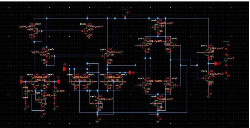
Fig. 2: Schematic Diagram of the Proposed Three Stage CMOS Comparator
Pre-Amplification Stage A.
The loads which are active in nature, along with a differential amplifier circuit forms the pre-amplification stage. Initially, the transconductance of amplifier which is differential in nature and resistance at the input side is considered for assigning the dimensions. Later, the values of NM0 and NM1 are chosen. Gain of this stage is defined by the transconductance of amplifier, which is differential in nature. The values of NM0 and NM1 define the value of capacitance at the input side. The length of all MOSFETs is chosen to be 100nm, considering speed as the prime factor. Offset voltages which are not necessary, occur due to the effect of channel length modulation. The width values of PM0 and PM2 are made higher, considering the width values of PM1 and PM3. This is done to improve the gain value of the first stage.
Using the sizes of the MOSFETs as given in the schematic diagram, the input voltages can be related to the current by
( ) (1)
(2)
Decision Stage: B.
(5)
The voltages of the switching point is given by the following expression
( ) ( ) (6) (7) Output Buffer Stage
C.
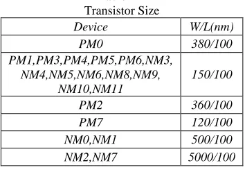
The last block of the comparator circuitry is the output block. It is nothing but the post-amplifier circuit. In this block, the decision block’s output is converted into a digital signal. The output block receives the input signal which is differential in nature. There should be no limitations for slewing. The MOSFET NM10 is connected serially with the decision stage. This enhances the average value of the output voltage. The MOSFET’s dimension can be of any arbitrary value. To enhance the decision stage’s output up to VTHN, the W/L ratio of NM7 is taken to be 5μm/100nm. The design parameters of the comparator topology implemented are shown in Table-1.
Table – 1 Transistor Size
Device W/L(nm)
PM0 380/100
PM1,PM3,PM4,PM5,PM6,NM3, NM4,NM5,NM6,NM8,NM9,
NM10,NM11
150/100
PM2 360/100
PM7 120/100
NM0,NM1 500/100 NM2,NM7 5000/100
III.
SIMULATION RESULTS
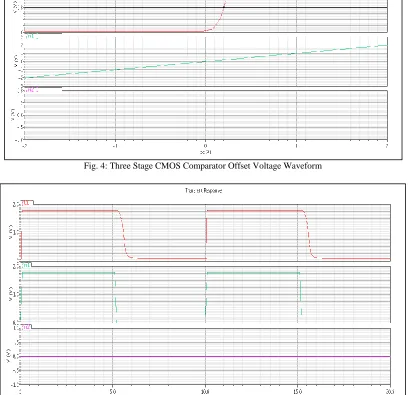
Fig. 3: Output Waveform of Comparator and Decision Circuit
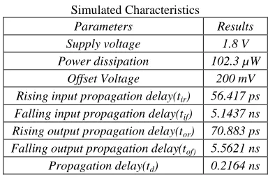
Falling output propagation delay(tof) 5.5621 ns
Propagation delay(td) 0.2164 ns
IV.
CONCLUSION
In this paper, a three stage CMOS comparator topology for low power and high speed applications is presented. A single comparator circuit has been built and tested. The circuit is designed and simulated in GPDK 90nm Technology with Cadence environment. Test results are obtained from the test structures designed for different parameters. It shows that the proposed design can work under 1.8V supply, with an offset voltage of 200mV, and a low power dissipation of 102.3µW is achieved.
REFERENCES
[1] P. E. Allen and D. R. Holberg, “CMOS Analog Circuit Design,” 2nd Edition, Oxford University, Oxford, 2007.
[2] D. A. Johns and K. Martin, “Analog Integrated Circuit Design,” John Wiley and Sons, Inc., New York, 1997.
[3] P. R. Gray and R. G. Meyer, “Analysis and Design of Analog Integrated Circuits,” 3rd Edition, John Wiley & Sons, Inc., Hoboken, 1993.
[4] B. Razavi, “Design of Analog CMOS Integrated Circuits,” Tata McGraw-Hill, Delhi, 2002.
[5] B.Razavi and B.A.Wooley, “Design techniques for high-speed high-resolution comparators,” IEEE J. Solid-State Circuits, vol. SC-27, pp.1916-1926,
Dec 1992.
[6] H. Nyquist, “Certain topics in telegraph transmission theory,” Transactions of the AIEE, Vol. 47, No. 2, 1928, pp. 617-644.
[7] M. Panchore and R. S. Gamad, “Low power and high speed CMOS comparator design using 0.18 μm technology,” International Journal of Electronic
Engineering Research, Research India Publications, Vol. 2, No. 1, 2010, pp. 71-77.
[8] G. Yongheng, C. Wei, L. Tiejun and W. Zongmin, “A novel 1GSPS low offset comparator for high speed ADC,” 5th International Joint Conference on