Volume 11, Issue 10 (October 2015), PP.16-27
Estimation of Crosstalk Noise for 2
RC and RLC Interconnects
in Deep Submicron VLSI Circuits
Md. Maniruzzaman
1, Alok Sarkar
2, Rafia Nishat Toma
3, Md. Tariq Hasan
41-4Electronics and Communication Engineering Discipline, Khulna University, Khulna-9208, Bangladesh
Abstract:- Crosstalk noises have been estimated both for RC and RLC interconnects, respectively, in deep submicron VLSI circuits. The 2π model approach has been employed. The victim line is considered as an RC or RLC line, and the aggressor line is placed near the victim line. The aggressor line is excited with a voltage pulse at the coupling location keeping the victim line quiet. Analytical expressions of the output crosstalk noise voltages have been derived, and then the values of the peak noise voltages have been calculated. Subsequently, simulation work by HSPICE has been performed. The result shows an output crosstalk peak noise estimation of 6.29% error on average and that of 5.77% error on average compared with HSPICE simulation both for 2π RC and RLC interconnects, respectively.
Keywords:- Crosstalk noise, Interconnect, Deep submicron, 2 model, Victim line, Aggressor line, VLSI circuit.
I.
INTRODUCTION
Continuous scaling of MOS transistor and the increase of circuit complexity are making the role of interconnect in deep submicron (DSM) VLSI circuits more prominent. DSM technology is the technology where transistors of smaller size with faster switching rates are used. Technologies beyond the feature sizes of 0.25 m are usually referred as DSM technologies. Several issues, such as, signal integrity, low-power design, high-density and design complexity, packing and testing, cost-effectiveness are challenging in DSM technology, where the signal integrity issue is very much critical. The major concerning signal integrity issues are crosstalk noise, crosstalk delay and electro-migration. These issues can lead to chip failure, if these issues are not addressed rightly in right time. In DSM technology, crosstalk noise has recently become more crucial due to capacitive coupling between lines/wires as well as inductive effect [1 – 3]. The line which suffers is referred to as victim, and the neighbouring line which contributes to coupling/inductive noise on the victim is referred to as aggressor. If the crosstalk noise effects on the victim line are large, they can propagate into storage elements that connect to victim line and can cause permanent errors. Intensive researches have been going on for proposing better models for accurate estimation of crosstalk noise for RC and RLC interconnects [1-6]. Different analytical models, such as, and L models,have been proposed taking R, L, C as lumped and/or distributed parameters in the lines/wires. Recently -model has become more popular. Along with analytical analysis, SPICE simulation in the circuit level has drawn special attraction due to time-saving as well as justification perspective.
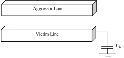
In this study, the 2π model approach has been employed for analytical study in time domain. The victim line is considered as an RC or RLC line. An aggressor line is placed near the victim line, as shown in Fig. 1. The aggressor line is excited with a voltage pulse, such as, a unit step input [2] for RC interconnect and the input reported by Sahoo et. el [3] for RLC interconnect at the coupling location keeping the victim line quiet. After analytical investigation, SPICE simulation in the circuit level has been performed using HSPICE software platform. The results obtained from analytical study have been compared with the results obtained by HSPICE simulation both for 2π RC and RLC interconnects, respectively. It reveals that the output of the investigation is appreciable.
Fig. 1: Layout of aggressor and victim lines
Aggressor Line
Victim Line
II.
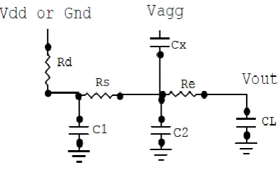
MATERIALS AND METHODS A. Derivation of Crosstalk Noise for 2 π RC InterconnectThe equivalent circuit of Fig. 1 is shown in Fig. 2, in the form of 2π type RC model, to derive the analytical expression of crosstalk noise voltage in time domain. This model contains two π type RC circuits – one type RC circuit is located before the coupling and the other is after the coupling. The victim driver is modelled by an effective resistance Rd and the other RC parameters are Cx, C1, Rs, C2, Re and CL, as shown in
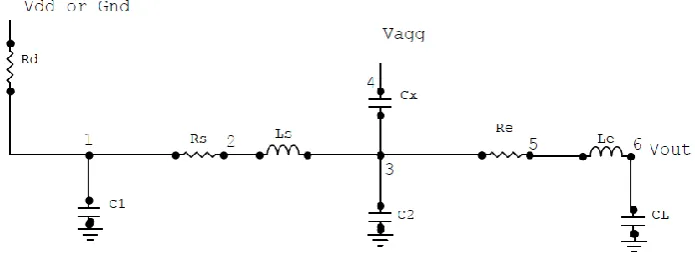
Fig. 2 which is redrawn, as shown in Fig. 3.
Fig. 2: Equivalent circuit of victim and aggressor lines in the form of 2 π type RC model
Fig. 3: Equivalent circuit of 2 π type RC model, redrawn from Fig. 2
From Fig. 3, the impedances Z1 at node 1 and Z2 at node 2 in s-domain are obtained as,
1 1
1
sR
C
R
Z
d d
(01)
L e s
SC
R
sC
R
Z
Z
1
1
1
1
2 1
2 (02
Therefore, the voltage V2(s) at node 2 across the impedance Z2 in s-domain is found as,
)
(
1
)
(
2 2
2
V
s
sC
Z
Z
s
V
aggx
Finally the output voltage Vout in s-domain becomes, L e L out
sC
R
sC
s
V
s
V
1
1
)
(
)
(
2
(04)Manipulating the Equations (01) – (04), Vout (s) can be represented in the form as,
)
(
)
(
0 1 2 2 3 1 2 2s
V
b
s
b
s
b
s
s
a
s
a
s
V
out agg
(05)The coefficient are defined as,
.
}
{
}
){
(
and
,
)
(
)
(
)
)(
(
,
1
,
,
)
(
2 1 1 1 2 2 2 1 2 1 2 0 2 1 2 2 1K
C
C
R
R
C
C
R
R
R
C
C
R
R
C
C
b
K
R
R
C
R
C
C
R
R
R
C
C
b
K
b
K
K
a
K
R
R
C
a
L s d L e d e L s d x s d L e L d s d x s d x
Using dominant-pole approximation method [3], the Equation (05) can be simplified in the form as,
)
(
)
(
11
V
s
b
s
b
s
a
s
V
agg oout
(06)Now applying unit step input with normalized Vdd = 1 in the aggressor, i.e.,
s
s
V
agg1
)
(
The Equation (06) becomes,
o out
b
s
b
a
s
V
1 1)
(
(07)Putting the values of a1, b1 and b0 in Equation (07), and then manipulating, we found Vout(s) as,
)
1
(
)
(
v v x outt
s
t
t
s
V
(08) Here, tx is the RC delay term from the upstream resistance of the coupling element and the coupling capacitance. And tv is the distributed Elmore delay [1] of victim line. Mathematically,)
(
)
(
)
)(
(
and
),
(
d s v x 2 d s d 1 L e L d ex
x
C
R
R
t
C
C
R
R
R
C
C
R
C
R
R
t
The output voltage shown in Equation (08) is in s-domain, and can be expressed in time domain as,
0
where
,
)
(
t
e
t
t
t
V
tvt
v x
out (09)
The Equation (09) reveals that the output crosstalk noise voltage decreases monotonically with the condition t≥0, and the maximum value of noise is,
v x
t
t
B. Derivation of Crosstalk Noise for 2 π RLC Interconnect
The equivalent circuit of Fig. 1 is shown in Fig. 4, in the form of 2π type RLC model, to derive the analytical expression of crosstalk noise voltage in time domain. This model contains two π type RLC circuits – one type RLC circuit is located before the coupling and the other is after the coupling. The victim driver is modelled by an effective resistance Rd and the other RLC parameters are Cx, C1, Rs, Ls, C2, Re, Le and CL, as
shown in Fig. 4 which is redrawn, as shown in Fig. 5.
Fig. 4: Equivalent circuit of victim and aggressor lines in the form of 2 π type RLC model
Fig. 5: Equivalent circuit of 2 π type RLC model, redrawn from Fig. 4
From Fig. 5, the impedances Z1 at node 1 and Z2 at node 3 in s-domain are obtained as,
1 1
1
sR
C
R
Z
d d
(11)
L e e s
s
sC
sL
R
sC
sL
R
Z
Z
1
1
1
1
2 1
2 (12)
Therefore, the voltage V2(s) at node 3 across the impedance Z2 in s-domain is found as,
)
(
1
)
(
2 2
2
V
s
sC
Z
Z
s
V
aggx
(13)
Finally the output voltage Vout in s-domain becomes,
1
1
)
(
)
(
2 2
L e e L out
C
L
s
R
sC
s
V
s
V
(14))
(
1
)
(
1 2 2 3 3 4 4 5 5 1 2 2 33
V
s
s
b
s
b
s
b
s
b
s
b
s
a
s
a
s
a
s
V
out
agg
(15)The coefficient are defined as,
)
(
)
)(
(
)}
(
)
){(
(
}
)
){(
(
)
)(
(
,
)
)(
(
)
(
),
(
,
1 2 1 1 1 1 2 2 1 1 1 1 2 3 1 1 2 4 2 5 1 1 2 1 3 s d L d L e s d x s d s L L e d L e s d s L e s d x L s d L e d s d L s e L e s d L e s L e s d x L e s d L e s d x L e s d x s d x s s d s d xR
R
C
C
R
C
R
R
R
C
C
b
C
R
R
L
C
C
R
C
R
C
L
C
R
R
L
C
R
R
R
C
C
b
C
C
L
R
C
L
C
R
C
L
R
C
L
R
C
R
C
R
R
C
L
L
C
L
R
R
C
C
b
C
R
C
L
R
C
L
C
R
R
C
C
b
C
L
R
R
C
C
b
R
R
C
a
L
C
R
R
a
C
L
R
C
a
Using dominant-pole approximation method [3], the Equation (15) can be simplified in the form as,
)
(
1
)
(
)
(
1 2 2 01
V
s
s
p
s
p
a
s
a
s
C
s
V
x aggout
(16)where,
0 1 1 2
,
1
0 1
and
0(
)
2
C
LL
eC
xa
b
R
eC
LC
xa
b
p
C
xa
b
R
eC
La
R
sR
dp
Now applying the input as reported by Sahoo et. el [3] in the aggressor, i.e.,
r r r r aggt
s
t
a
s
a
t
a
s
t
s
V
1
1
1
)
(
1 2 1 2The Equation (16) becomes,
r r r r x outt
s
t
a
s
a
t
a
s
t
s
p
s
p
a
s
a
s
C
s
V
1
1
1
1
)
(
1 2 1 2 1 2 2 0 1 (17)Again using dominant-pole approximation method [3], the Equation (17) can be simplified in the form as, 3 9 3 8
)
(
s
A
s
A
s
V
out (18)where,
3 3 3 1 08
a
a
t
C
A
r x and
3 3 3 1 09
The output voltage shown in Equation (18) is in s-domain, and can be expressed in time domain as, t
t out
t
A
e
A
e
V
3 39 8
)
(
(19)The Equation (19) reveals that the output crosstalk noise voltage decreases exponentially as honey-comb of two factors, and the peak value of noise can be found as,
peak
peak t
t
peak
A
e
A
e
V
3 39 8
(20)where,
3 1 0 3
3 1 0 3
3 3
ln
1
a
a
a
a
t
peakC. HSPICE Simulation
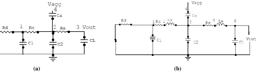
We use HSPICE for circuit simulation and the circuits for simulation are shown in Figs. 6(a) and (b) for RC and RLC interconnects, respectively. The maximum output crosstalk noise voltage expressions are found in Equations (10) and (20) for RC and RLC interconnects, respectively.
(a) (b)
Fig. 6: Equivalent circuit for simulation by HSPICE: (a) for RC interconnect and (b) for RLC interconnect
III.
RESULTS AND DISCUSSIONWe simulated the output noise voltage by using HSPICE and compared the simulated results with the analytical results observed in 2π RC and 2π RLC models.
A. Noise Estimation for 2 RC Interconnect
Unit step input is used in aggressor line keeping victim line as quiet for noise estimation in 2 RC interconnect. Fig. 6(a) is used for simulation by HSPICE. Fig. 7 shows the output noise voltage in time domain across victim capacitor (CL) at node 3 of Fig. 6(a) for 2 RC interconnect. From constant 40 ms the voltage is
Fig. 7: Output noise voltage in time domain across victim capacitor CL at node 3 of Fig. 6(a) for 2 RC
interconnect, where Rd = 50 , Re = 20 , Rs = 20 , Cx = 150 fF, CL=10 fF
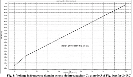
Fig. 8 shows the voltage across victim capacitor CL at node 3 of Fig. 6(a) with respect to frequency.
The figure shows that voltage is approximately increasing with respect to increasing frequency.
Fig. 8: Voltage in frequency domain across victim capacitor CL at node 3 of Fig. 6(a) for 2 RC
interconnect, where Rd = 50 , Re = 20 , Rs = 20 , Cx = 150 fF, CL=10fF
We perform the simulation program by HSPICE. Fig. 9 shows the output crosstalk noise voltage waveforms in frequency domain of RC interconnect in DSM VLSI circuit for unit step aggressor input. While performing simulation by HSPICE, we use the maximum frequency of 10 GHz. When the frequency is increasing, the noise voltage is decreasing gradually, as seen in the Fig. 9.
Fig. 9: Output crosstalk noise voltage waveform in frequency domain by HSPICE simulation for RC interconnect, where Rd = 50 , Re = 20 , Rs = 20 , C1 = 50 fF, C2 = 100 fF, Cx = 150 fF and CL = 10 fF
After simulation work, we calculated the peak values of the output crosstalk noise voltage using the Equation (10). The peak values of the output crosstalk noise voltage for both the calculated and simulated data are summarized in Table I. And then we compared the simulated data with the calculated data which are shown as % of error and % of average error in Table I. The table shows that the average % of error is 6.29%, which is good enough compared to the other results published in the literature [1], [2], [4], [5], [7-9]. The comparison is shown in Table II.
Table I: Comparison of Output Crosstalk Noise Peak Voltage for RC Interconnect Sl.
No.
R
d ()s
R
() e
R
()
1
C
(fF) x
C
(fF)
2
C
(fF) L
C
(fF) peak
V
(v)(HSPICE) peak
V
(v)Calculated Error (%)
Average Error (%) 1 50 20 20 50 150 100 10 0.4101058 0.50 17.97
6.29 2 100 50 50 50 150 100 15 0.4880701 0.49 0.39
3 150 70 70 50 150 100 20 0.4936848 0.48 2.16 4 200 100 100 50 150 100 25 0.4907008 0.47 3.60 5 250 120 120 50 150 100 30 0.4797421 0.45 7.33
Table II: Comparison of Average % of Error for RC Interconnect with Published Literature
Our Work
Ref. [1] Ref. [2] Ref. [4] Ref. [5] Ref. [7] Ref. [8] Ref. [9]
Average Error (%)
6.29 6 2.2 5 14 4.4 8.4 13
0 0.2 0.4 0.6 0.8 1 1.2 1.4 1.6 1.8 2
x 10-10 10-1
100 101 102
Time (sec)
M
a
x
im
u
m
C
ro
s
s
ta
lk
N
o
is
e
(
v
o
lt
)
DEV Model
HEY Model Circuit simulation
2 Pi Model
Fig. 10: Comparison of Maximum Crosstalk Noise Voltage of 2 RC Interconnect for unit step input
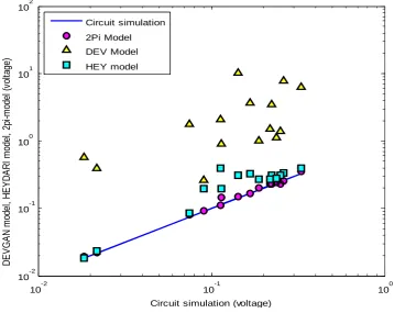
Fig. 11 shows the scatter diagrams which compare the Devgan, Heydari and 2π models with circuit simulations. As seen in the figure, the estimation accuracy of the Devgan model compared with the circuit simulation is not high. The estimation accuracy of the Heydari model is higher than that of the Devgan model. And the 2π model gives very good estimation, i.e., the diagram shows that the estimation accuracy of 2π model is higher than that of the other models, compared with circuit simulation.
10-2 10-1 100
10-2 10-1 100 10
1
102
Circuit simulation (voltage)
D
E
V
G
A
N
m
od
el
,
H
E
Y
D
A
R
I
m
od
el
,
2p
i-m
od
el
(
vo
lta
ge
)
Circuit simulation 2Pi Model DEV Model HEY model
B. Noise Estimation for 2 RLC Interconnect
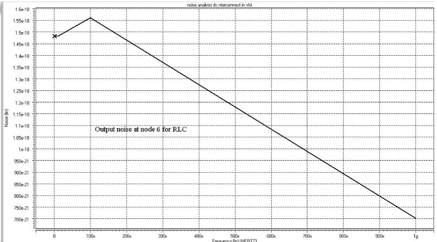
The Input reported by Sahoo et. el [3] and imported for Equation (17) is used in aggressor line keeping victim line as quit for noise estimation in 2 RLC interconnect. Fig. 6(b) is used for simulation by HSPICE. Fig. 12 shows the output noise voltage in time domain across victim capacitor (CL) at node 6 of Fig. 6(b) for 2 RLC
interconnect. From constant 100 ms the voltage is increasing so fast and then after saturation label at 160 ms again the voltage is decreasing directly and at this time the voltage will be constant with respect to increasing time.
Fig. 12: Output noise voltage in time domain across victim capacitor CL at node 6 of Fig. 6(b) for 2 RLC
interconnect, where Rd = 50 , Rs = R1a = 20 , Re = R1v = 20 , Ls = 302 nH, Le = 302 nH, C1 = 50 fF, C2
= 100 fF, Cx = 150 fF and CL = 10 fF
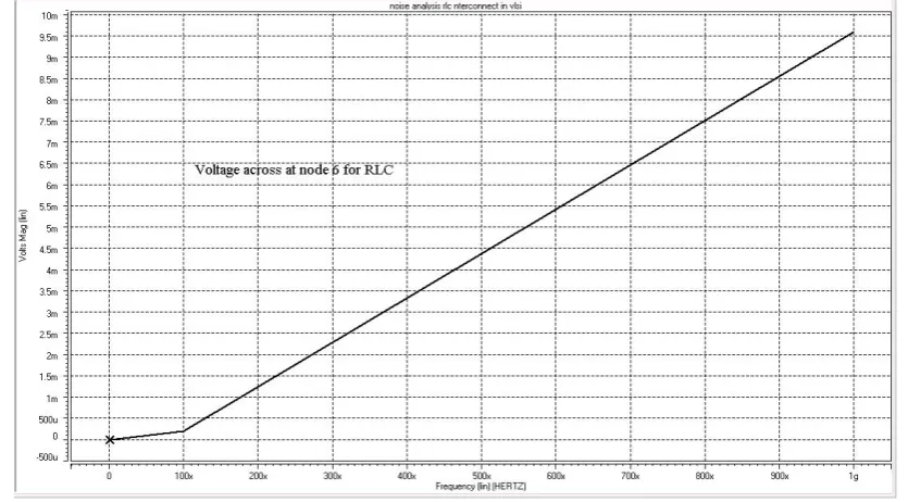
Fig. 13 shows the voltage across victim capacitor CL at node 6 of Fig. 6(b) with respect to frequency.
The figure shows that voltage is approximately increasing with respect to increasing frequency.
Fig. 13: Voltage in frequency domain across victim capacitor CL at node 6 of Fig. 6(b) for 2 RLC
interconnect, where Rd = 50 , Rs = R1a = 20 , Re = R1v = 20 , Ls = 302 nH, Le = 302 nH,
We perform the simulation program by HSPICE. Fig. 14 shows the output crosstalk noise voltage waveforms in frequency domain of RLC interconnect in DSM VLSI circuit for aggressor input reported by Sahoo et. el [3] and imported for Equation (17). While performing simulation by HSPICE, we use the maximum frequency of 1 Ghz. When the frequency is increasing, the noise voltage is decreasing gradually, as seen in the Fig. 14.
Fig. 14: Output crosstalk noise voltage waveform in frequency domain by HSPICE simulation for RLC interconnect, where Rd = 10 , Rs = R1a = 10 , Re = R1v = 10 , Ls = L1a= 0.5 nH,
Le = L1v = 0.5 nH, C1 = 50 fF, C2 = 100 fF, Cx = 150 fF and CL = 5 fF
After simulation work, we calculated the peak values of the output crosstalk noise voltage using the Equation (20). The peak values of the output crosstalk noise voltage for both the calculated and simulated data are summarized in Table III. And then we compared the simulated data with the calculated data which are shown as % of error and % of average error in Table III. The table shows that the average % of error is 5.77%, which is good enough compared to the other results published in the literature [1], [3], [6], [11 – 14]. The comparison is shown in Table IV.
Table III: Comparison of Output Crosstalk Noise Peak Voltage for RLC Interconnect
Sl. No.
Tr (psec)
Rd = Rth ()
R1a=R2a =R1v=R2v
()
L1a=L2a =L1v=L2v
(nH)
Cla=Clv (fF)
Vpeak (v) (HSPICE)
Vpeak (V) Calculated
Error (%)
Averag e % Error
1 50 10 10 0.5 5 20.0236 18.27 8.749
5.77
2 100 50 20 1 10 34.1940 34.65 1.320
3 150 100 50 10 15 51.5173 54.44 5.370
4 200 150 70 20 20 62.4839 67.41 7.300
Table IV: Comparison of Average % of Error for RLC Interconnect
Our Work
Ref. [1] Ref. [3] Ref. [6] Ref. [11] Ref. [12] Ref.
[13]
Ref. [14]
IV.
CONCLUSIONIn this work, the output crosstalk noise voltages for both RC and RLC interconnects in DSM VLSI circuits are analysed and estimated. We use 10 GHz frequency for RC interconnects and 1 GHz frequency for RLC interconnects. In order to reduce output crosstalk noise, operating at 10 GHz and 1 GHz frequency for RC and RLC interconnect, respectively, are proposed along with 2 modelling approach. It is observed that the crosstalk noise is effectively reduced to 6.29% for RC interconnects and 5.77% for RLC interconnect with 2 modelling approach. These results are good enough compared to the other results published in the literature.
REFERENCES
[1]. P. V. Hunagund, and A. B. Kalpana, “Crosstalk noise modeling for RC and RLC interconnects in deep submicron VLSI circuits”, Journal of Computing, vol. 2, no. 4, pp. 60-65, Apr. 2010.
[2]. V. Maheshwari, Annushree, R. Kar, D. Mandal, and A. K. Bhattacharjee, “Noise modeling for RC interconnects in deep submicron VLSI circuit for unit step input ”, Journal of Electron Devices, vol. 11, pp. 632-636, Nov. 2011.
[3]. S. Sahoo, M. Datta, and R. Kar, “Accurate crosstalk analysis for RLC on-chip VLSI interconnect”, International Journal of Electrical and Electronics Engineering, vol. 5, no. 4, pp. 302-310, Nov. 2011. [4]. Anushree, and V. Maheshwari, “Crosstalk noise reduction using wire spacing in VLSI RC global
interconnects”, Journal of Electron Devices, vol. 20, pp. 1755-1760, Sep. 2014.
[5]. M. Hashimoto, M. Takahashi, and H. Onodera, “Crosstalk noise estimation for generic RC trees”, IEICE Trans. Fundamentals, vol. E86-A, no.12, pp. 2965-2973, Dec. 2003.
[6]. D. Kaur, and V. Sulochana, “Crosstalk minimization in VLSI interconnects”, International Journal of Reconfigurable and Embeded systems, vol. 2, no. 2, pp. 89-98, Jul. 2003.
[7]. J. Zhang, and E. G. Friedman, “Crosstalk noise model for shielded interconnects in VLSI-based circuits”, in Proc. IEEE International SOC Conference, 2003, p. 243.
[8]. P. Heydari, and M. Pedram, “Capacitive coupling noise in high–speed VLSI circuits”, IEEE Transactions on Computer-Aided Design of Integrated Circuits and Systems, vol. 24, no. 3, pp. 478-488, Mar. 2005.
[9]. A. Kahng, S. Muddu, and D. Vidhani , “Noise and delay estimation for coupled RC interconnects”, in Proc. IEEE AISC/SOC, 1999, p. 1.
[10]. A. Devgan, “Efficient coupled noise estimation for on-chip interconnects”, in Proc. IEEE/ACM International Conference on Computer-Aided Design, 1997, p. 147.
[11]. P. Heydari, and M. Pedram, “Analysis and reduction of capacitive coupling noise in high-speed VLSI circuits”, in Proc. ICCD 2001, 2001, p. 104.
[12]. Y. Cao, X. Huang, D. Sylvester, N. Chang, and C. Hu, “A new analytical delay and noise model for on-chip RLC interconnect”, in Proc. IEDM 00, 2000, paper 35.5.1, p.823.
[13]. T. K. Tang, and E. G. Friedmnan, “Peak crosstalk noise estimation in CMOS VLSI circuits”, in Proc. ICECS’99, 1999, p. 1539.