Int. J. Nanosci. Nanotechnol., Vol. 14, No. 4, Dec. 2018, pp. 297-306
Design and Test of New Robust QCA
Sequential Circuits
A. Rezaei*
Department of Electrical Engineering, Kermanshah University of Technology, Kermanshah, Iran.
(*) Corresponding author: [email protected], [email protected] (Received: 07 November 2016 and Accepted: 15 April 2018)
Abstract
One of the several promising new technologies for computing at nano-scale is quantum-dot cellular automata (QCA). In this paper, new designs for different QCA sequential circuits are presented. Using an efficient QCA D flip-flop (DFF) architecture, a 5-bit counter, a novel single edge generator (SEG) and a divide-by-2 counter are implemented. Also, some types of oscillators, a new edge-triggered K-pulse generator (KPG) and a negative K-pulse generator (NPG) are presented for implementation in QCA. The robust layouts of proposed circuits are designed, implemented and simulated using QCADesigner software without any wire crossing. The fault effects at the output of proposed DFF due to the missing cell defects are analyzed. Also, the robustness of the proposed QCA designs with respect to temperature variations is examined. The proposed designs are compared with the previous QCA works and conventional CMOS technology. The simulation results confirm that the novel QCA architectures work properly and can be simply used in designing of QCA sequential circuits.
Keywords: Quantum-dot cellular Automata, QCADesigner, Sequential Circuits, Simulation.
1. INRODUCTION
Research into nanoscale electronics has increased significantly over the last decade. VLSI technology is going to approach a scaling limit in deep nanometer regime. International Technology Road-map for Semiconductors (ITRS) [1] reports several possible technology solutions to replace the current CMOS technology. Quantum-dot cellular automata (QCA) may overcome some of the limitations of current technologies, because it not only gives a solution at the nanoscale, but also it offers new methods of computation and information transformation [2-6]. In conventional logic circuits information is transferred by electrical current, but QCA operates using the Columbic interaction that connects the state of one QCA cell to the state of its neighbors. High density, fast switching speed, and low power dissipation are the advantages of QCA circuits over the current CMOS technology. QCA sequential circuits
single-layer synchronous counters were proposed. Also, by cascading the proposed T flip-flop and a suitable level converter a QCA-compatible structure for falling edge triggered T flip-flop was achieved. In [12], using a robust 2:1 multiplexer efficient level triggered and edge triggered QCA flip-flops and memory cell with set/reset ability were introduced. In [13], a robust and efficient QCA design of synchronous counters was proposed. For this means, an innovative design of level-sensitive DFF and an appropriate “edge-to-level” converter were introduced by utilizing
inherent capabilities of QCA
implementations. In [14], two well-organized JK flip-flop designs and synchronous counters with different sizes were presented.
In this paper, novel designs for different QCA sequential circuits are presented. These designs are introduced for the first time.
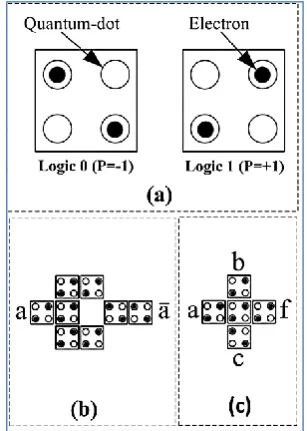
The fundamental unit of QCA is the QCA cell [15,16]. A QCA cell (shown in Figure 1a) can be viewed as a set of four charge containers or quantum-dots, positioned at the corners of a square and two extra mobile electrons (free electrons), which can quantum mechanically tunnel between the dots, but not cells. Due to the electrostatic repulsion, the two free electrons only can occupy the corners of the QCA cell, resulting in two specific polarizations as shown in Figure 1a. By using cell polarization P=+1 to represent logic ”1” and P=-1 to represent logic ”0”, binary information can be encoded. By arranging the QCA cells in some proper arrangements, it is possible to build logical elements and also transfer binary information. QCA logic circuits is usually constructed with the binary wire, the inverter Gate and the three-input majority Gate [17, 18]. The QCA wire is a row of QCA cells, in which a binary signal propagates from left-to-right because of electrostatic interactions between adjacent cells. To make a complete logical set, we need an inverter Gate as shown in Figure
1b. The majority Gate can be built by five QCA cells as shown in Figure 1c, in which the cells a, b and c are the inputs and the cell f is the output with the following logic function [19, 20]:
. . . ( , , )
f a b b c a c M a b c (1) Logic AND and OR functions can be implemented from the majority Gate by setting an input permanently to “0” or “1” values, respectively. The majority Gate is not a complete Gate in QCA technology. Using the inverter Gate and the three-input majority Gate every QCA logic circuit can be implemented.
Figure 1. The QCA (a): cell (b): inverter Gate (c): three-input majority Gate.
2. PROPOSED QCA DESIGNS
neighbor cells have a center to center distance of 20 nm and quantum dots have 5 nm diameters.
2.1. D Flip-Flop
Flip-flops are the basic storage element in sequential logic. They are one of the main building blocks of digital circuits, which are used in the computer and communications, and many other types of systems. One of the most fundamental Flip-flops is the D flip-flop (DFF), which captures the value of input D at a definite portion of the clock cycle (Clock). At other times, the output Q does not change. The D flip-flop is widely used. It is also known as a "data" or "delay" flop. The D flip-flop can be viewed as a memory cell; a zero-order hold or a delay line. In Figure 2, the characteristic table and the symbol of D flip-flop are shown, where the inputs are D and C (Clock), the output is Q, and Qo
means the previous state of Q. Using Figure 2, the output function of DFF and its equivalent expression based on the inverter and three-input majority Gates can be obtained by the following equation:
. .
( ( , , 1), ( , , 1), 1) o
o
Q C D C Q
M M C D M C Q
(2)
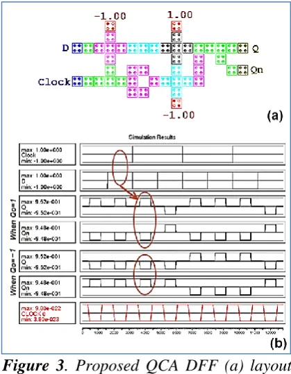
In Figure 3, one possible implementation of DFF and its simulation results for both Qo=-1 and Qo=+ 1 are shown.
Figure 2. DFF (a) circuit symbol (b) characteristic table.
QCADesigner software (Bistable approximation engine with default parameters) is used to design and simulation of the proposed DFF. The proposed DFF has the following specifications: the number of cells 46, the
occupied area 0.0512 µm2 and 4 phases
input to output delay.
Figure 3. Proposed QCA DFF (a) layout (b) simulation results.
To solve the problem of physical level implementation of QCA clock signal, a more realistic clock distribution should be adopted. Figure 4 shows a logic-propagation technique for the 2-D diagonal wave scheme (2DDWave) [22].
Figure 4. Clocking for the 2-D wave propagation [22].
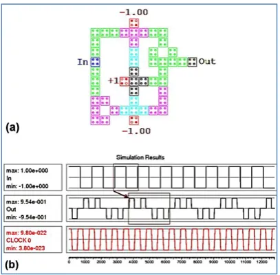
signals only from two zones (north and west) and pass its outputs to the other two zones (south and east). Figure 5 shows the layout of proposed DFF with 2-D wave clocking and its simulation results.
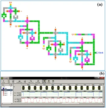
To show the functionality of the proposed DFF in Figure 3, a 5-bit up counter is designed [13]. Figure 6 shows the layout and simulation results of proposed 5-bit counter. This counter is implemented with 368 QCA cells. It has an area of 0.81 um2
and 6.5 clock cycles delay.
Recently, fault-tolerant properties of QCA circuits have been presented by several researchers [23, 14, 24]. The cell misplacement, cell misalignment, cell missing deposition and extra or additional cell defects are main defects in QCA implementations. In this section we present missing cell defects and identify the test vectors for detection of all faults for the proposed DFF.
Figure 5. Proposed DFF with 2-D wave clocking (a) Layout (b) simulation results.
Through all simulations, a particular cell labeled with the number i (i =1,2, …, 42) (shown in Figure 7) is deleted in the original (defect-free) configuration of the proposed DFF and the new configuration is simulated using QCADesigner with Bistable engine.
The simulation results show that only deleting the cells with the numbers 3, 5, 7, 9, 14, 17, 20, 25 and 40 results faulty output in the output Q and deleting the other cells results no faulty output in the output Q. Also, for the input set {Clock D} ={00, 01, 10, 11} all distinct faulty outputs in the output Q are obtained: {0101, 1111, 0000, xxxx, 1100}, where x means Q has a polarization of “0” (Null). For detecting the effects of these defects, a test sequence can be utilized as: {Clock D} = {01, 11} (for the defect-free output 0001 when Q0=0) and {Clock D} = {00, 10, 11} (for
the defect-free output 1101 when Q0=1).
These test vectors can detect any cell missing defects in the proposed DFF layout.
Figure 7. Layout of the proposed DFF for analysis of missing cell defects.
2.2. Single Edge Generator
Frequency dividers and (rising or falling) single edge generator (SEG) are some of DFF applications. By putting C=D in Equation (2), a rising SEG can be created. In this case, if the input is “In” and the output is “out” then:
. .
.
o
o o
out In In In out
In In out In out
(3)
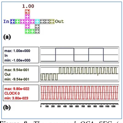
In Figure 8, the QCA implementation and simulation results of proposed SEG in QCADesigner are shown.
Figure 8. The proposed QCA SEG (a) layout (b) simulation results.
The proposed SEG has the following specifications: the number of cells 16, the occupied area 0.0161 µm2 and 3 phases input to output delay. In the proposed SEG, three phases after raising the input, the output rises and then remains in this state. This input to output delay can be changed by placing n-phase and m-phase wires in the input and output, respectively. In this case, in the proposed SEG, (3+m+n) phases after raising the input, the output rises and then remains in this state. Also, by placing an inverter Gate in the output, a falling SEG can be realized.
2.3. Divide-by-2 Counter
Another application of DFF is binary divider for frequency division or a divide-by-2 counter. By putting DQo in Equation (2), a divide-by-2 counter can be created. In this case, if the input is “In” and the output is “out”, then:
o o
o Inout In out
out In
out . .
Figure 9. Proposed QCA divide-by-2 counter (a) layout (b) simulation results.
It can be seen from Figure 9b, that the output has a frequency that is exactly one-half that of the frequency of input “In”. In other words, the circuit produces frequency division as it now divides the input frequency by a factor of two. This can produce a type of counter called ripple counter, in which the clock pulse triggers the first flip-flop whose output triggers the second flip-flop and so on.
2.4. Oscillators
An electronic oscillator is an electronic circuit that produces a repetitive, oscillating electronic signal, often a sine wave or a square wave. Oscillators are widely used in many electronic devices. Oscillators are often characterized by the frequency of their output signals. The logical function for a selectable oscillator is given by:
(5)
o out In Out .
where “In” is the activation input and “Out” is the output of selectable oscillator. By putting “In”=1 a permanent oscillator can be realized. Also, by using a SEG and a selectable oscillator, a positive-edge-triggered oscillator can be created, which is sensitive to the rising edge of its input. In Figure 10, the circuit diagram, QCA layout and simulation results of proposed oscillators are shown, where “Select OSC”, “OSC” and “Edge OSC” are stand
for the output of selectable, permanent and positive-edge-triggered oscillators, res-pectively. The proposed selectable and permanent oscillators have the following specifications: the number of cells 16, the occupied area 0.016 µm2 and 2 phases input to output delay. Also, the proposed positive-edge-triggered oscillator has the following specifications: the number of cells 38, the occupied area 0.049 µm2 and 7 phases input to output delay.
2.5. K-pulse Generator (KPG)
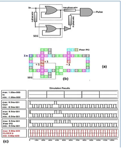
In Figure 11a, the circuit diagram of a positive-edge-triggered K-pulse generator is presented, where:
(6)
4
m n
K
The proposed K-pulse generator is composed of two SEGs, one AND Gate, one inverter Gate, a wire with one phase delay (one-phase wire), an n-phase wire and an m-phase wire. In this circuit, the first output pulse is appeared six phases after the first rising edge of the input. In Figure 11b, the QCA layout of a positive-edge-triggered 4-pulse generator is shown. Also, Figure 11c shows the simulation results of proposed positive-edge-triggered K-pulse generator for K=1 (1-pulse generator), K=2 (2-pulse generator) and K=4 (4-pulse generator (Four PG)) in QCADesigner software, where Out1, Out2 and “Four PG” are stand for the outputs of proposed 1, 2 and 4-phase generators, respectively.
The proposed layout shown in Figure 11b has the following specifications: the number of cells 63, the occupied area 0.063 µm2 and 6 phases input to output
delay.
2.6. Negative Pulse Generator (NPG)
Figure 10. (a) Layout of proposed selectable oscillator (b) layout of proposed permanent oscillator (c) circuit diagram of proposed positive-edge-triggered oscillator (d) layout of proposed positive-edge-triggered oscillator (e) simulation results of proposed oscillators.
Figure 11. (a) Circuit diagram of proposed positive-edge-triggered K-pulse generator (b) layout of proposed 4-pulse generator (c) simulation results of proposed 1, 2 and 4-pulse generators.
This sort of circuit is encountered frequently, and many logic designers have met it and solved it one way or another usually by using a single-shot or some sort of logic delay line. Our circuit description only provides for a single stable output value. The negative pulse is generated on the rising edge of the input, and will automatically complete before stability returns. The equations for the circuit are:
1 2
2 1 2
Q Y P y
Y y Py
(7)
These equations are implemented in Figure 12.
Figure 12. Negative pulse generator (a) circuit diagram (b) proposed QCA layout (b) simulation results.
3. RESULTS AND DISCUSSIONS
The consumption power in the QCA arrays is 10-10W per input bit. In this research, DFF, single edge generator, positive-edge-triggered oscillator, negative pulse generator and edge-triggered K-pulse generator designs have 2, 1, 1, 1 and 1 inputs, respectively and thus the consumption powers of them are 10
2 10 W,
W
10
10 , 10W
10 , 10W
10 and 10W
10 , respectively. Fault-tolerant properties and characteristics of QCA for metal and molecular implementations have been reported by several researchers [25, 26]. The cell misalignment, cell misplacement, cell missing deposition, stuck-at-Z and extra or additional cell defects are the identified defects in QCA circuits. In this section, simulation of missing cell defects for the proposed NPG are presented. Through all simulations, a particular cell labeled with the number i (i = 1, 2, …, 50) (shown in Figure 12) is deleted in the original (defect-free) configuration of the proposed NPG, and the new configuration is simulated using QCADesigner with its coherence vector engine with the following parameters: temperature 1 K, relaxation time 1 fs, time step 0.1 fs, total simulation
time 70 ps, clock high 9.8×10⁻²² J, clock low 3.8×10⁻²³ J, clock shift 0, clock amplitude factor 2, radius of effect 80 nm, relative permittivity 12.9, layer separation 11.5 nm, Euler method, and randomized simulation order. The simulation results show that deleting the cells with the numbers 1, and 3 results no faulty output in output “Q”. Deleting the cells with the numbers 4-7 and 11, 12, 16 and 17 converts the proposed NPG to a positive-edge-triggered oscillator. Deleting the cells with the numbers 1-3, 8, 9, 14, 18-27, 38, 40, 42-46, and 48-50 results no faulty output in the output Q. Temperature has different effects on different QCA circuits. The robustness (producing high polarization correct response in different temperatures) of the proposed QCA designs is presented. This can be done with the measurement of output cells polarization (when the output is correct) in different temperature. Figure 13 shows the robustness results for the divide-by-two, Four PG and NPG designs. The simulation results show that all proposed QCA designs are able to produce correct results in the temperature range from 1K to 20K. As it can be seen, the performance of the proposed NPG is better than the other ones. It should be mentioned that the outputs of the proposed designs will not be broken down when temperature passes from 1K to 20K. Therefore, the proposed QCA designs are robust designs.
Figure 13. The robustness of proposed QCA designs.
Figure 14. Layout of negative pulse generator implemented with 0.13μm CMOS technology.
Table 1. Comparison with 0.13 μm CMOS technology.
NPG Approximated
area (μm2)
Clock frequency (GHz)
Proposed QCA layout
0.052 28.5
0.13μm CMOS Technology
16.9 <3
From Table 2 it is clear that our presented QCA layout has a relatively good performance. From the obtained results, it can be seen that the proposed designs work satisfactory and produce correct outputs with highly polarized
signals, which can provide a high drivability for QCA circuits.
Table 2.Comparison with the previous QCA works.
References Area (um2)
Complexity (cell count)
Delay (clock cycle) Level triggered
DFF [12]
0.05 48 1
Falling edge triggered DFF [12]
0.09 84 2.75
Rising edge triggered DFF [12]
0.09 84 2.75
Dual edge triggered DFF [12]
0.14 120 3.25
DFF-(I) [13] 0.1 74 1.5
DFF-(II) [13] 0.02 28 0.5
Proposed DFF 0.05 46 1.25
4. CONCLUSIONS
Quantum-dot cellular automata (QCA) with its unique specifications reduces the physical limit of CMOS devices implementation. Thus it encourages researchers to utilize it in designing of integrated circuits. In this paper, new efficient designs for QCA DFF, single edge generator, oscillators, negative pulse generator and edge-triggered K-pulse generator were presented. The proposed designs were implemented and simulated using QCADesigner software without any wire crossing methods. Also, the robustness of proposed QCA designs was tested. The results showed that these designs work properly and can be simply used in designing of QCA sequential circuits.
REFERENCES
1. ITRS (International Technology Roadmap for Semiconductors), www.itrs.net/, (2016).
2. Ganesh, E. N., Lal, K., Rangachar, M. J. S., (2008). “Implementation of Quantum cellular automata combinational and sequential circuits using Majority logic reduction method”, Int. J. Nanotech. and Applications, 2(1): 89-106.
3. Zhang, R., Walnut, K., Wang, W., Jullien, G., (2004). “A method of majority logic reduction for quantum cellular automata”, IEEE Trans. on Nanotech., 3: 443-450.
5. Safavi A., Mosleh, M., (2016). “Presenting a New Efficient QCA Full Adder Based on Suggested MV32 Gate”, International Journal of Nanoscience and Nanotechnology, 12(1): 55-69.
6. Dallaki, H., Mehran, M., (2015). “Novel Subtractor Design Based on Quantum-Dot Cellular Automata (QCA) Nanotechnology”, International Journal of Nanoscience and Nanotechnology, 11(4): 257-262. 7. Swapna, M., Hariprasad, A., (2016). “Design of Sequential Circuit Using Quantum-Dot Cellular Automata
(QCA)”, International Journal of Advanced Engineering Research and Science (IJAERS), 3(9): 95-100. 8. Lim, L. A., Ghazali, A., Yan, S. C. T., Fat, C. C., (2012). “Sequential circuit design using Quantum-dot
Cellular Automata (QCA)”, IEEE International Conference on Circuits and Systems (ICCAS), DOI: 10.22161/ijaers/3.9.15: 162-167.
9. Gladshtein, M., (2016). “Quantum-dot cellular automata serial decimal processing-in-wire: Run-time reconfigurable wiring approach”, Microelectronics Journal, 55:152–161.
10. Rezaei, A., Saharkhiz, H., (2016). “Design of low power random number generators for quantum-dot cellular automata”, Int. J. Nano Dimens., 7(4): 308-320.
11. Angizi, Sh., Moaiyeri, M. H., Farrokhi, Sh., Navi, K., Bagherzadeh, N., (2015). "Designing quantum-dot cellular automata counters with energy consumption analysis", Microprocessors and Microsystems, 39(7): 512-520.
12. Hashemi, S., Navi, K., (2012). "New robust QCA D flip flop and memory structures", Microelectronics Journal, 43: 929–940.
13. Abutaleb, M. M., (2017). "Robust and efficient quantum-dot cellular automata synchronous counters", Microelectronics Journal., 61: 6-14.
14. Angizi, Sh., Sayedsalehi, S., Roohi, A., Bagherzadeh, N., Navi, K., (2015). "Design and verification of new n-Bit quantum-dot synchronous counters using majority function-based JK flip-flops", Journal of Circuits, Systems and Computers, 24(10): 1550153-1-1550153-17.
15. H¨anninen, I., Takala, J., (2010). “Binary Adders on Quantum-Dot Cellular Automata”, J Sign Process Syst., 58: 87-103.
16. Lakshmil, S., Athishi, G., Ganesh, M. C., (2010). “Design of Subtractor using Nanotechnology Based QCA”, ICCCCT, Ramanathapuram, India, 384-388.
17. Navi, K., Maeen, M., Foroutan, V., Timarchi, S., Kavehei, O. A., (2009). “Novel low-power full-adder cell for low voltage”, Integration, the VLSI j., 42: 457-467.
18. Ahmad, F., Bhat, G.M., Ahmad, P.Z., (2014). “Novel Adder Circuits Based on Quantum-Dot Cellular Automata (QCA)”, Circuits and Systems., 5: 142-152.
19. Abedi, D., Jaberipur, G., and Sangsefidi, M., (2015). “Coplanar Full Adder in Quantum-Dot Cellular Automata via Clock-Zone-Based Crossover”, IEEE transactions on nanotechnology, 14(3): 497-504. 20. Santra, A. S., Santra, S., (2015). “Design and Simulation of Quantum Cellular Automata Based XOR Gate
With Optimize Complexity and Cell Count”, Journal of Emerging Technologies and Innovative Research (JETIR), 2(1): 110-116.
21. http://www.mina.ubc.ca/qcadesigner, (2016).
22. Vankamamidi,V., Ottavi, M., Lombardi, F., (2008). “Two-dimensional schemes for clocking timing of QCA circuits”, IEEE Transactions on Computer aided Design of Integrated Circuits and Systems, 27(1): 34-44. 23. Chabia, A. M., Roohi, A., Khademolhosseini, H., Sheikhfaal, Sh., Angizi, Sh., Navid, K., DeMara, R. F.,
(2017), "Towards ultra-efficient QCA reversible circuits", Microprocessors and Microsystems, 49: 127-138. 24. Hayati, M., Rezaei, A., (2015). “Design of novel efficient adder and subtractor for quantum‐dot cellular
automata”, International Journal of Circuit Theory and Applications, 43 (10): 1446-1454.
25. Tahoori, M. B., Momenzadeh, M., Huang, J., Lombardi, F., (2004). “Testing of quantum cellular automata”, IEEE Transactions on Nanotechnology, 3(4):432–442.