IJSRR, 8(1) Jan. – Mar., 2019 Page 2871
Research article Available online www.ijsrr.org
ISSN: 2279–0543
International Journal of Scientific Research and Reviews
Reduction of THD Using Three and Five Level Diode Clamped
Multilevel Inverter
S.
Flora Viji Rose*
*Dr. Sivanthi Aditanar College of Engg., Tiruchendur, Tamilnadu, India. Email: [email protected]
ABSTRACT
This paper presents a five level and three level diode clamped multilevel inverter topology which can be used for low medium power industrial applications. The topology of five level and three level diode clamped multilevel inverter is tested using MATLAB. Circuit operation is presented, simulated & Total Harmonic Distortion is analyzed. To obtain sinusoidal output voltage with low harmonics, multicarrier PWM technique is used for diode clamped multilevel inverter.
KEYWORDS:
Diode clamped multilevel inverter, PWM technique*Corresponding Author
S.Flora Viji Rose,
Department of E.E.E.,
Dr.Sivanthi Aditanar College of Engineering, Tiruchendur – 628215,
Tamilnadu, INDIA.
IJSRR, 8(1) Jan. – Mar., 2019 Page 2872
problem can be eliminated by increasing the switches, diodes and capacitors. This type of inverters provides high efficiency because the fundamental frequency used for all the switching devices.
DRIVE SYSTEM DESCRIPTION
In the conventional method ordinary PWM method is used. Here switching frequency causes more amount of switching loss. These problems are corrected using three phase diode clamped multilevel inverter. Here switching losses are reduced when compared to the conventional technique.
Figure.1: Multilevel inverter based drive circuit
PRINCIPLE OF OPERATION
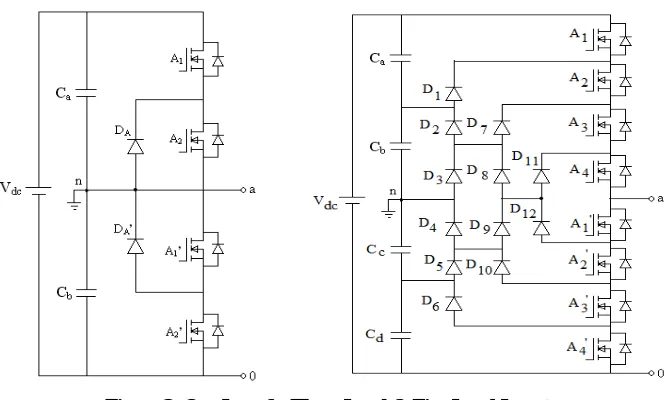
To produce an output voltage in staircase shape, consider one leg of a three-level inverter, as shown in Figure.2. The steps to produce the three-level voltages are as follows.
1. For an output voltage level
V
ao=V
dc, turn on all upper leg switches A1 and A2.2. For an output voltage level
V
ao=V
dc/2,
turn on one upper switch A2 and one lower switchA1’.
IJSRR, 8(1) Jan. – Mar., 2019 Page 2873
Figure.2: One Leg of a Three Level & Five Level Inverter
Table.1. shows the voltage levels for three level inverter and their corresponding switch states. Switch is on means state condition is 1, 0 means the switch is off. There are two opposite switch pairs in each phase.
Table 1: Voltage level for three level inverter and their Switching states
Output vao Switch states
A1 A1’ A2 A2’
Vdc 1 1 0 0
Vdc/2 0 1 1 0
0 0 0 1 1
To produce an output voltage in staircase shape, consider one leg of a five-level inverter, as shown in Figure.2. The steps to produce the five-level voltages are as follows.
1. For voltage level
V
ao= V
dc, turn on all upper switches A1 – A4.2. For voltage level
V
ao= 3V
dc/4
, turn on three upper switches A2 – A4 and one lower legswitch A1’.
3. For voltage level
V
ao= V
dc/2
, turn on two upper switches A3 and A4 and two lower switchesA1’ and A2’.
4. For voltage level
V
ao= V
dc/4
, turn on one upper switch and three lower switches A1’– A3’.5. For voltage level
V
ao= 0
, turn on all lower switches A1’– A4’.IJSRR, 8(1) Jan. – Mar., 2019 Page 2874
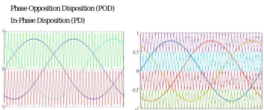
flexible than SVM methods. Multicarrier PWM method can be categorized into three groups:
Alternative Phase Opposition Disposition (APOD)
Phase Opposition Disposition (POD)
In-Phase Disposition (PD)
Figure.3: In-Phase Disposition Technique for 3-Level & 5-Level Multilevel Inverters
Figure.3. demonstrates the sine-triangle method for a three-level & five level inverters. Therein, the modulation signal is compared with N-1 triangle waveforms.
SIMULATED CIRCUITS AND WAVEFORMS
The triggering circuit is formulated based on the three phase sinusoidal modulation waves, Va, Vb, and
Vc. Three sine wave sources have been obtained with same frequency and amplitude but displaced 120° out of
the phase with each others. For carriers wave sources block parameters, the time values of each
carrier waves are set to [0, (1/2000)*1/2, 1/2000] while the outputs values are set according to the
disposition of carrier waves. After comparing, the output signals of comparator are transmitted to the
MOSFET switches.
IJSRR, 8(1) Jan. – Mar., 2019 Page 2875 Figure.4: Gate Pulses for Leg A Switches.
Simulated model for entire circuit is shown in Figure.5.
Figure.5: Simulated Circuit
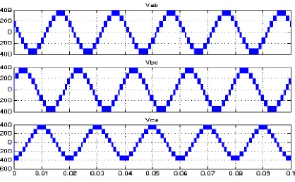
IJSRR, 8(1) Jan. – Mar., 2019 Page 2876 Figure.6: Output Line-Line Voltage for 3-Level Inverter
The FFT plot of the output voltage for three level inverter is shown in Figure.7. The plot shows that the harmonic content present in the output voltage is low.
Figure.7: FFT for 3-Level Inverter
IJSRR, 8(1) Jan. – Mar., 2019 Page 2877 Figure.8: Output Line-Line Voltage for 5-Level Inverter
The FFT plot of the output voltage for five level inverter is shown in Figure.9. The plot shows that the harmonic content present in the output voltage is very low compared to three level inverter.
Figure.9: FFT for 5-Level Inverter
Table 3: Reduction of THD by varying inverter level
Number of levels THD (%)
Three level 12.70
Five level 3.76
CONCLUSION
IJSRR, 8(1) Jan. – Mar., 2019 Page 2878
Trans. on Industrial Applications, 1981; l(17): 518–523.
3. L. Tolbert and T. G. Habetler, Novel multilevel inverter carrier-based PWM method,” IEEE Trans. on Industrial Applications, 1999; 35: 1098–1107.
4. G. Carrara, S. G. Gardella, M. Archesoni, R. Salutari and G. Sciutto, A new multi-level PWM method: A theoretical analysis, IEEE Trans. on Power Electronics, 1992; 7(3): 497– 505.
5. B.P.McGrath and D.G.Holmes, Multicarrier PWM strategies for multilevel inverters, IEEE Trans. on Industrial Electronics, 2002; 49(4): 858 – 867.