Graphene-loaded metal wire grating for deep
and broadband THz modulation in total
internal reflection geometry
Y
IWENS
UN1,
R
ICCARDOD
EGL’I
NNOCENTI2,
D
AVIDA.
R
ITCHIE2,
H
ARVEYE.
B
EERE2,
L
ONGX
IAO2,3,
M
ICHAELR
UGGIERO4,
J.
A
XELZ
EITLER5,
R
AYKOI.
S
TANTCHEV6,
D
ANNIC
HEN7,
Z
HENGCHUNP
ENG7,
E
MMAM
ACP
HERSON6,8,
X
UDONGL
IU1*1National-Regional Key Technology Engineering Laboratory for Medical Ultrasound, Guangdong Key
Laboratory for Biomedical Measurements and Ultrasound Imaging, Department of Biomedical Engineering, School of Medicine, Shenzhen University, Shenzhen 518060, China
2Cavendish Laboratory, University of Cambridge, J J Thomson Avenue, CB3 0HE, United Kingdom 3Department of Electrical Engineering and Computer Science, Massachusetts Institute of Technology,
Cambridge, Massachusetts 02139, USA
4Department of Chemistry, University of Vermont, 82 University Place, Burlington, VT 05405, USA 5Department of Chemical Engineering and Biotechnology, University of Cambridge, Pembroke Street,
Cambridge CB2 3RA, United Kingdom
6Department of Electronic Engineering, The Chinese University of Hong Kong, Hong Kong, China 7Key Laboratory of Ministry of Education for Optoelectronic Devices and Systems, College of
Optoelectronic Engineering, Shenzhen University, Shenzhen 518060, China Department of Physics,
8University of Warwick, Gibbet Hill Road, Coventry, CV4 7AL, United Kingdom *[email protected]
Abstract: We employed a metallic wire grating loaded with graphene and operating in total internal reflection (TIR) geometry to realise deep and broadband THz modulation. The non-resonant field enhancement effect of the evanescent wave in the TIR geometry and in the subwavelength wire grating was combined to demonstrate a ~77% modulation depth (MD) in the frequency range of 0.2-1.4 THz. This MD, achieved electrically with SiO2/Si gated
graphene device, was 4.5 times higher than the device without metal grating in transmission geometry. By optimizing the parameters of metallic wire grating, the required sheet conductivity of graphene for deep modulation was lowered to 0.87 mS. This work has potential applications in THz communication and real-time THz imaging.
© 2018 Optical Society of America under the terms of the OSA Open Access Publishing Agreement
1. Introduction
plasmonic crystal structure was also reported for the THz signal amplification and modulation [11, 12]. The electrical graphene devices can provide MHz level modulation speed, which is important for rapid THz imaging. However, the electrical approach suffers from low modulation depth (MD) [13-15]; assistant structures to improve the MD bring in narrowband features [16-18]. Other designs for THz modulators have also been reported, such as a metamaterial integrated liquid crystal design, which showed a MD of 75% but at a single frequency; high-speed THz modulators based on graphene were reported [10, 15], but again the MD was low and the bandwidth was limited. Ion-gel gated graphene is able to deeply modulate THz signals but with very slow operation speed [19-21]. The broadband field enhancement effect in a subwavelength metal grating has been theoretically [22] and experimentally explored: Shi et al. used ion-gel gated graphene integrated with a metal wire grating to achieve a MD of ~84%, but at an extremely high conductivity of 5.4 mS [20]. The operation speed of the ion-gel device was infeasible for high-speed THz modulation. A method that can deeply modulate the THz signal using a low sheet conductivity of graphene is thus desired. Our previous work has demonstrated that TIR geometry can outperform the standard transmission geometry for THz modulation, requiring lower conductivity to achieve the same MD over a broadband range [23]. However, a bare graphene modulator, even in the TIR geometry, can only provide ~40% broadband MD. The required sheet conductivity for a ~100% MD is still as high as 5 mS in the TIR geometry with silicon as the substrate material [23]. A new approach is needed to further reduce the required conductivity, while maintaining its operational bandwidth. Combining the non-resonant field enhancement effect in the evanescent wave in the TIR geometry in a metal grating structure can lead to stronger enhancement effects, rendering the possibility for efficient THz modulation. We have illustrated the extraordinary features of a metal wire grating in the TIR geometry in our previous work [24]: passive and active THz polarization convertors were demonstrated using the phase transition material, vanadium dioxide (VO2), integrated with a metal wire grating in
the TIR geometry [25].
In this work, we successfully extend the advantageous behavior of metal wire gratings to a THz graphene modulator in a TIR geometry for efficient and broadband THz modulation. This paper is structured as follows: in sections 2 and 3, a novel approach combining the non-resonant enhancement effect in the evanescent wave in the TIR geometry and in the subwavelength metal wire grating was proposed and simulated. The theory to describe the reflection coefficient from the metal wire grating integrated graphene modulator in the TIR geometry is presented; in sections 4 and 5, metal wire grating integrated graphene modulators were fabricated and measured in the TIR geometry based on the theoretical model. The device achieved approximately 77% MD in the frequency range of 0.2 to 1.4 THz, which was 4.5 times higher than the graphene device without metal grating in transmission geometry. High MD is possible with lower sheet conductivity of graphene by optimizing the metal grating parameters. This type of modulator can be easily extended to large-scale modulator arrays to spatially modulate THz signals for compressive sensing imaging applications.
2. Theory
High-resistivity SiO2/Si was chosen as the substrate to reduce the attenuation of the THz
signal. The metal wire grating worked as a contact electrode allowing a gate voltage to be applied simultaneously on the graphene. We chose s-polarized incident THz light so as to have its electric field perpendicular to the grating direction, as shown in Fig. 1(b). The evanescent wave at the TIR interface (air/Si interface) was confined in the gaps of the metal grating (no electric field in the metal). The electric field intensity in the grating slit was further enhanced. Therefore, the absorption of graphene was significantly increased enhancing the MD of the graphene device. However, the theory to describe the field enhancement effect of the metal grating and its corresponding MD in TIR geometry was hitherto absent. Here, we start the theoretical derivation from the boundary conditions of the electromagnetic wave.
The boundary conditions (s-polarization) integrated along the reflection interface without a metal grating and energy balance at the reflection interface can be written as:
i r t
E E E+ = , (1)
i r t a
j
= + +
j
j j
, (2)where Ei, Er and Et are the incident, reflected and transmitted electric field in s-polarization; as detailed in Ref [26], ji, jr and jt are the incident, reflected and transmitted energy flux, respectively. ja is the absorbed energy flux of graphene due to Joule heat. Next, we rewrite Eq. (2) in the form of electric field in reflection configuration in the case without metal grating:
2 2 2 2
0cn1cos iEi 0cn1cos iEr 0cn2cos tEt sEt
ε θ =ε θ +ε θ +σ , (3)
where ε0 is vacuum permittivity, c is the speed of light in vacuum, n1 is the refractive index of
a dense material, n2 is the refractive index of a less dense material, σs is the sheet conductivity
of graphene, θi is the incident angle and θt is the transmitted angle (note we assume the incident angle is equal to the reflected one here). When the metal grating is integrated into the system, the graphene in contact with the grating is short-circuited, reducing the effective area of the graphene by a factor of g/P. In the case of s-polarized incident light (electric field perpendicular to the grating slits), the electric field amplitude is P/g time stronger in the grating gaps than without the grating. In general, the absorbed energy is η times higher [20]. The absorbed energy flux has no angle dependence. Thus, Eq. (3) becomes:
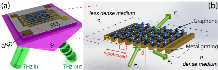
Fig. 1. (a) Graphene-loaded metal wire grating modulator in the TIR geometry. The graphene device was deposited on high-resistivity SiO2/Si substrate and placed on a Si prism. The conductivity of graphene was adjusted by the
voltage between GND and metal grating. The incident THz signal was in s-polarization. (b) Diagram of the metal grating loaded graphene structure of Fig. 1(a). The medium below the metal grating is the dense medium (n1) and above the metal grating is the less dense medium (n2). The THz signal is incident from the dense medium to the
[image:3.612.118.494.91.212.2]2 2 2 2 0cn1cos iEi 0cn1cos iEr 0cn2cos tEt sEt
ε θ ′ =ε θ ′ +ε θ ′ + ⋅η σ ′ , (4)
where E′r and E′t are the reflected and transmitted electric fields when the metal grating influence is accounted for. Combing Eq. (1), Eq. (4) and Snell’s law sinθt=(n1/n2)sinθi, the
reflection coefficient of s-polarized incident THz light with graphene and metal grating has the same formalism as in our pervious paper [9]. When the incident angle is supercritical,
cosθt becomes an imaginary number and we obtain:
2 2 2
1 1 2 0
2 2 2
1 1 2 0
cos sin
cos sin
i i s
r s
i i i s
n i n n Z
E r
E n i n n Z
θ θ η σ
θ θ η σ
− ⋅ − − ⋅
′
= =
+ ⋅ − + ⋅ , (5)
where Z0 (377 Ω) is the impedance of vacuum. Comparing Eq. (5) with the equation of the
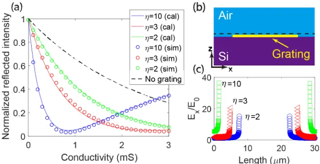
conductive interface TIR geometry without a metal grating [23], the required sheet conductivity of graphene for the same reflectivity is reduced by 1/η due to the metal grating. In Eq. (5), the conductivity of graphene layer effectively influences the reflection of the THz signal. The calculation results are shown in Fig. 2(a); with less than 1 mS sheet conductivity change, the reflected intensity of the THz signal varies between 1~0.03.
3. Simulation
Commercial software (COMSOL Multiphysics) was used to verify Eq. (6). Si and air were chosen as the dense and less dense materials, as SiO2/Si is a typically used substrate for
high-speed graphene devices [10]. The incident angle was set as 30° from Si to air, which was supercritical. The metal grating period was set as 30 μm. The gap width was set as 15 μm, 10
μm and 3 μm, which corresponded to an enhancement factor (η) of 2, 3 and 10 respectively. The simulation and calculation results are shown in Fig. 2(a). The theoretical results from Eq. (6) and simulation results match very well. When η increases from 2 to 10, the required sheet conductivity for a low reflection decreases from 3 mS to less than 1 mS. For η = 10 (gap of
Fig. 2. (a) Simulation and calculation results of reflected intensity from graphene/metal grating. The solid lines are calculation results and the dots are simulation results with different enhancement factors (η). The black dashed lines are the calculation results without a metal grating. (b) Simulation
structure of metal grating in the TIR geometry without graphene. The simulation electric field is polarized along the x direction. The black dashed line is to monitor the electric field amplitude in the simulations. (c) Simulated E-field enhancement of THz wave with metal grating with various
[image:4.612.146.475.303.472.2]3 μm), the required sheet conductivity is only 0.87 mS to achieve a minimum normalized reflected intensity of ~3%. In the structure without metal grating, the reflected intensity at 0.87 mS is still ~70%. The enhancement factor of the evanescent wave was also studied by simulation software. The results are shown in Fig. 2 (b) and (c). The electric field at the edge of metal grating has the highest enhancement factor of the incident electric field. There is no electric field in the metal grating, thus there is no enhancement factor in the grating area (as shown in Fig. 2(c), around x=15 µm). In our simulations, the highest enhancement factor is ~40 when η=10. The required sheet conductivity of graphene for a strong attenuation can be further reduced by increasing η, but a smaller grating period to wavelength (P/λ) ratio is required [20, 22]. This will bring challenges in device fabrication by standard photolithography techniques.
4. Experiment
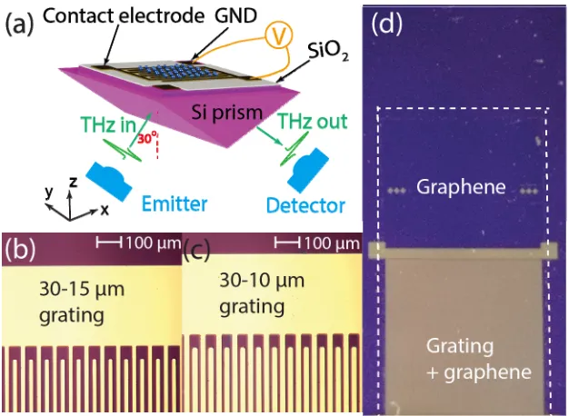
The graphene modulator was placed on a high-resistivity Si prism (isosceles triangle, each base angle is 30°, as shown in Fig. 3 (a)). A 0.5×0.5 cm size metal wire grating was fabricated on a 2×2 cm size SiO2/Si (square resistivity > 6K Ω·cm, double side polished) substrate using
standard photolithography and metalized with 5 nm thick Ti and 200 nm thick gold. Two types of metal gratings were fabricated: 30 μm period, 15 μm gap width (abbreviated as 30-15
μm grating in this paper) and 30 μm period, 10 μm gap width (abbreviated as 30-10 μm grating), as shown in Fig. 3 (b) and (c). The fabrication of the 30 μm period, 3 μm gap device is too challenging for our photolithography facilities. A piece of 1×0.5 cm size graphene was transferred on the metal grating, which covered half of the metal grating and left the other grating half as reference (shown in Fig. 3 (d)). Using the same piece of graphene for the reference helps ensure the graphene was in the same doping level and thus has the same sheet conductivity. The metal wire grating also worked as a contact electrode for applying a voltage on the graphene between the GND electrode. A –60 V was applied to the GND electrode first and swept to +60 V. A reflection THz time-domain spectroscopy system from Menlo Systems (TERA-K15) was used for the TIR geometry experiments with the THz incident at 30° to the normal (Fig. 3(a)). More details of the experimental setup are reported in [27]. To image the metal wire loaded graphene device, the emitter and detector pair are raster scanned along the x and y direction (as shown in Fig. 3(a)). In this case, the THz signal was normally incident onto the Si prism. The bottom surface of the SiO2/Si substrate was cleaned carefully and
5. Results and discussion
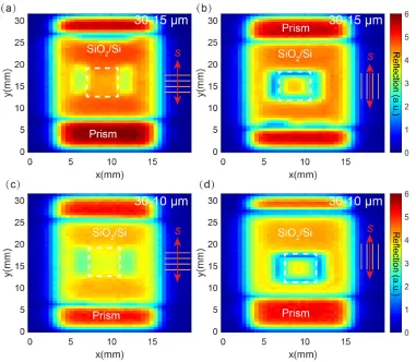
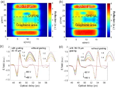
Figs. 4 (a) and (b) show the THz peak-to-peak images of the 30-15 μm grating without graphene for perpendicular and parallel aligned THz polarization respectively. The prism surface has the largest reflected peak-to-peak value. The THz signal reflected from the top surface of device has minor reflection loss due to the small air gap between the prism and the device. The reflected THz signal from the top surface of the prism doesn’t have any reflection loss caused by the small air gap, thus it has the largest peak-to-peak value (red colour). The white dashed squares highlight the metal grating areas. In Fig. 4(a), the electric field direction is perpendicular to the slit direction of the grating. The grating area shows a slightly lower peak-to-peak value compared to the SiO2/Si area. In Fig. 4(b), the grating area has a similar
reflection to that of the surrounding SiO2/Si area. This phenomenon was verified by our
previous study, when the electric field is parallel to the grating slits, the grating area performs as a uniform metal layer; when the electric field is perpendicular to the grating slits, the grating has little influence to the reflected electric field [24]. The slight decrease of peak-to-peak value in Fig. 4 (a) comes from the bandwidth limitation of the grating area. Similar results can be observed in Fig. 4 (c) and (d). Further, applying the grating structure to improve the performance of THz modulation introduced very small losses as can been seen in Figs 4(a) and (c), and outperformed many alternatives. Thus, the main losses in this modulator design arise from the insertion losses into the silicon prism, which can be minimized by using an anti-reflection coating. The multi-reflection loss from the air gap between SiO2/Si substrate
and Si prism can be minimized by tightly pressing the device to the prism or using a liquid in between them. The central brighter area in Fig. 4(b) and (d), arises because the THz spot was only partly covered by the metal grating at the edges of metal grating. In the reflected signal in the TIR geometry, the metal grating covered area and the SiO2/Si surface covered area
[image:6.612.157.470.91.320.2]caused a different phase change, thus the superposition of the reflected THz signal from metal grating and SiO2/Si parts introduced a polarization conversion [24].
Fig. 3. Schematic of the experimental setup and photograph of the metal grating integrated graphene device. (a) Schematic of graphene modulator in TIR geometry. (b) and (c) are photographs of the metal grating structure. (d) Photograph of the graphene area, showing clearly the graphene covered
Fig. 5(a) and (b) show the images of the peak-to-peak value of reflected THz signal of bare-graphene and bare-graphene-loaded metal grating devices. The black dashed lines highlight the graphene areas. In Fig. 5 (a), the left half of the graphene covered area contains bare graphene and the right half contains a loaded metal grating. In Fig. 5(a) and (b), the graphene-loaded metal grating areas show higher attenuation than those with bare graphene areas, because of the enhanced E-field concentration. The 30-10 μm grating device (Fig. 5(b)) has lower reflected electric field amplitude to the 30-15 μm grating device (Fig. 5(a)), as expected from the theoretical framework developed in the section 2. Figs. 5(c) and (d) show the reflected waveforms of the 30-15 μm grating and 30-10 μm grating respectively. The solid (dashed) lines in these two figures show the results of graphene areas with (without) the metal grating. The voltage applied to the graphene was swept from –60 V to 60 V. The conductivity of graphene can be tuned by applying an external applied voltage [28]. The graphene sample in this experiment was p-doped, the reflected electric field amplitude had the least attenuated value at –60 V and the highest attenuated value at 60 V. This trend was expected considering the biasing configuration and that similar values are routinely reported in literature. The voltage was not applied over ±60 V to avoid breaking down the SiO2 insulation layer. The
[image:7.612.118.499.93.425.2]amplitude of THz signal at –60 V was taken as the baseline in calculating the MD. In Fig. 5(c)
and (d), the solid lines have higher relative peak-to-peak change compared with dashed lines. Because the sheet conductivity of graphene is the same in the area with or without metal grating, it indicates the increase in the MD comes from the effect of metal grating. After the above measurements, the two graphene devices were rotated by 90° to make the grating slits be parallel to the electric field direction (as shown in Fig. 4 (b) and (d)). The applied voltage on the graphene was again swept from –60 V to 60 V, no modulation effect was observed.
Fig. 5. Experimental results of metal grating integrated graphene device. (a) and (b) THz peak-to-peak images of 30-15 μm and 30-10 μm grating device without applying a voltage. The graphene transferred on the metal grating is highlighted with white dashed lines. The right side of graphene area is with metal grating; the left side of graphene area is without covering metal grating. (c) and (d) are reflected waveforms by changing gate voltages from –60 V to +60 V for 30-15 μm and 30-10 μm grating devices with (solid) and without grating (dashed). Four insets in Fig. (c) and (d)
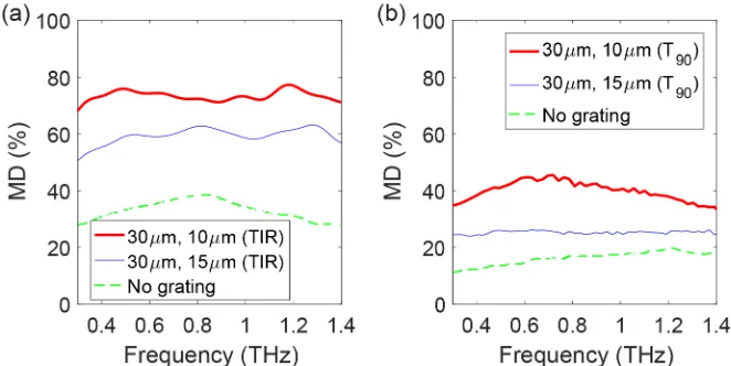
Fig. 6 (a) and (b) show the MDs in the frequency domain for the TIR and transmission geometries respectively. In the TIR geometry, the peak-to-peak value of the reflected E-field of the graphene without gratings, with 30-15 μm gratings and with 30-10 µm gratings is ~3, ~2.6, ~2.1 at -60 V, respectively, and ~2.6, ~1.73, ~1.1 at 60 V. Further, in the frequency range of 0.2 to 1.4 THz, the graphene area without the metal grating achieved an average MD of 33%; the MD of 30-15 μm device is ~60%; the MD of 30-10 μm device is ~77%. Placing the same devices in transmission geometry and applying the same voltages, the corresponding MDs of the bare graphene, graphene-loaded 30-15 μm grating, 30-10 μm grating and bare graphene were only 17%, 25% and 45%, respectively. Compared to the MD of the graphene area without a metal grating in the TIR geometry, the integration of the 30-10 μm metal grating enhanced the MD by 2.3 times. Compared to the MD of the graphene area without the metal grating in the transmission geometry, the 30-10 μm metal grating integrating graphene device improved the MD by 4.5 times. The increase of the MD goes up with the enhancement factor η, these results follow the trend of our theoretical predictions..
6. Conclusions
In this work, we have presented a novel approach to enhancing the THz modulation from graphene via the field confining properties of subwavelength metallic gratings in combination with the increased sensitivity of conductive surfaces offered by the TIR geometry. After discussing the theory, we simulated how the grating parameters affect the MD enhancement factor; most notably in the subwavelength regime the fill ratio was inversely proportional to the enhancement factor. Then we experimentally showed that the graphene integrated metal grating device outperformed the bare graphene device and realised deep modulation of 77% over the broadband range of 0.2 to 1.4 THz. Such ideas can be extended, by creating individually controllable grating blocks, to perform spatial modulation of a THz beam. This can then be used in conjunction with single-element detectors for compressive sensing imaging [6, 29, 30]. Given the modulation speed of the solid-state graphene devices [10, 15], this work offers itself as a viable technique towards real-time THz imaging.
Funding
National Natural Science Foundation of China (NSFC) (61575125, 61671308), the Guangdong Foundation of Outstanding Young Teachers in Higher Education Institutions
Fig. 6 (a) and (b) are the MDs of the two devices in the TIR and in transmission geometry (T90). The red solid line is the MD of graphene integrated with 30-10 μm grating; the blue
[image:9.612.153.484.97.263.2](YQ2015141), Guangdong Special Support Program of Top-notch Young Professionals (2015TQ01R453), CUHK Global travel fund, the Hong Kong Research Grants Council (14201415), and the Hong Kong Innovation and technology fund (ITS/371/16), the UK Engineering and Physical Sciences Research Council (EPSRC) for funding (EP/N022769/1).
Acknowledgments
We thank Qiang Wang from Professor Zhengchun Peng’s group at Shenzhen University for his help in the fabrication of the grating devices.
References
1. W. L. Chan, J. Deibel, and D. M. Mittleman, "Imaging with terahertz radiation," Reports on progress in physics 70, 1325 (2007).
2. C. Yu, S. Fan, Y. Sun, and E. Pickwell-MacPherson, "The potential of terahertz imaging for cancer diagnosis: A review of investigations to date," Quantitative imaging in medicine and surgery 2, 33 (2012). 3. C. Jansen, S. Wietzke, O. Peters, M. Scheller, N. Vieweg, M. Salhi, N. Krumbholz, C. Jördens, T.
Hochrein, and M. Koch, "Terahertz imaging: applications and perspectives," Applied optics 49, 48-57 (2010).
4. F. Ferri, D. Magatti, L. Lugiato, and A. Gatti, "Differential ghost imaging," Physical review letters 104, 253603 (2010).
5. B. Sun, M. P. Edgar, R. Bowman, L. E. Vittert, S. Welsh, A. Bowman, and M. Padgett, "3D computational imaging with single-pixel detectors," Science 340, 844-847 (2013).
6. R. I. Stantchev, B. Sun, S. M. Hornett, P. A. Hobson, G. M. Gibson, M. J. Padgett, and E. Hendry, "Noninvasive, near-field terahertz imaging of hidden objects using a single-pixel detector," Science advances 2, 1600190 (2016).
7. R. Al Hadi, H. Sherry, J. Grzyb, Y. Zhao, W. Forster, H. M. Keller, A. Cathelin, A. Kaiser, and U. R. Pfeiffer, "A 1 k-pixel video camera for 0.7–1.1 terahertz imaging applications in 65-nm CMOS," IEEE Journal of Solid-State Circuits 47, 2999-3012 (2012).
8. I. Escorcia, J. Grant, J. Gough, and D. R. S. Cumming, "Uncooled CMOS terahertz imager using a metamaterial absorber and pn diode," Optics Letters 41, 3261-3264 (2016).
9. X. Liu, E. P. J. Parrott, B. S.-Y. Ung, and E. Pickwell-MacPherson, "Exploiting total internal reflection geometry for efficient optical modulation of terahertz light," APL Photonics 1, 076103 (2016).
10. R. Degl’Innocenti, D. S. Jessop, C. W. Sol, L. Xiao, S. J. Kindness, H. Lin, J. A. Zeitler, P. Braeuninger-Weimer, S. Hofmann, and Y. Ren, "Fast modulation of terahertz quantum cascade lasers using graphene loaded plasmonic antennas," ACS Photonics 3, 464-470 (2016).
11. M. Chen, F. Fan, L. Yang, X. Wang, and S. Chang, "Tunable Terahertz Amplifier Based on Slow Light Edge Mode in Graphene Plasmonic Crystal," IEEE Journal of Quantum Electronics 53, 1-6 (2017). 12. F. Fan, S. Chen, W. H. Gu, X. H. Wang, and S. J. Chang, "Active terahertz plasmonic crystal waveguide
based on double-structured Schottky grating arrays," Applied Physics Letters 105, 101 (2014).
13. T. Kleine-Ostmann, K. Pierz, G. Hein, P. Dawson, M. Marso, and M. Koch, "Spatially resolved measurements of depletion properties of large gate two-dimensional electron gas semiconductor terahertz modulators," Journal of Applied Physics 105, 093707 (2009).
14. B. Sensale-Rodriguez, R. Yan, M. M. Kelly, T. Fang, K. Tahy, W. S. Hwang, D. Jena, L. Liu, and H. G. Xing, "Broadband graphene terahertz modulators enabled by intraband transitions," Nature communications 3, 780 (2012).
15. D. S. Jessop, S. J. Kindness, L. Xiao, P. Braeuninger-Weimer, H. Lin, Y. Ren, C. Ren, S. Hofmann, J. A. Zeitler, and H. E. Beere, "Graphene based plasmonic terahertz amplitude modulator operating above 100 MHz," Applied Physics Letters 108, 171101 (2016).
16. G. Liang, X. Hu, X. Yu, Y. Shen, L. H. Li, A. G. Davies, E. H. Linfield, H. K. Liang, Y. Zhang, S. F. Yu, and Q. J. Wang, "Integrated Terahertz Graphene Modulator with 100% Modulation Depth," ACS Photonics 2, 1559-1566 (2015).
17. W. Gao, J. Shu, K. Reichel, D. V. Nickel, X. He, G. Shi, R. Vajtai, P. M. Ajayan, J. Kono, and D. M. Mittleman, "High-contrast terahertz wave modulation by gated graphene enhanced by extraordinary transmission through ring apertures," Nano letters 14, 1242-1248 (2014).
18. B. Sensale-Rodriguez, R. Yan, S. Rafique, M. Zhu, W. Li, X. Liang, D. Gundlach, V. Protasenko, M. M. Kelly, and D. Jena, "Extraordinary control of terahertz beam reflectance in graphene electro-absorption modulators," Nano letters 12, 4518-4522 (2012).
19. Y. Wu, C. La o vorakiat, X. Qiu, J. Liu, P. Deorani, K. Banerjee, J. Son, Y. Chen, E. E. Chia, and H. Yang, "Graphene Terahertz Modulators by Ionic Liquid Gating," Advanced Materials 27, 1874-1879 (2015).
21. Z. Miao, Q. Wu, X. Li, Q. He, K. Ding, Z. An, Y. Zhang, and L. Zhou, "Widely Tunable Terahertz Phase Modulation with Gate-Controlled Graphene Metasurfaces," Physical Review X 5, 041027 (2015). 22. A. Novitsky, A. M. Ivinskaya, M. Zalkovskij, R. Malureanu, P. U. Jepsen, and A. V. Lavrinenko,
"Non-resonant terahertz field enhancement in periodically arranged nanoslits," Journal of Applied Physics 112, 074318 (2012).
23. X. Liu, Z. Chen, E. P. Parrott, B. S. Y. Ung, J. Xu, and E. Pickwell MacPherson, "Graphene based terahertz light modulator in total internal reflection geometry," Advanced Optical Materials 5, 1600697 (2017).
24. X. Liu, X. Chen, E. P. J. Parrott, and E. Pickwell-MacPherson, "Exploiting a metal wire grating in total internal reflection geometry to achieve achromatic polarization conversion," Photon. Res. 5, 299-304 (2017).
25. X. Liu, X. Chen, E. P. J. Parrott, C. Han, G. Humbert, A. Crunteanu, and E. Pickwell-MacPherson, "Invited Article: An active terahertz polarization converter employing vanadium dioxide and a metal wire grating in total internal reflection geometry," APL Photonics 3, 051604 (2018).
26. S. Bauer, "Optical properties of a metal film and its application as an infrared absorber and as a beam splitter," American journal of physics 60, 257-261 (1992).
27. X. Liu, Z. Chen, E. P. Parrott, B. S. Y. Ung, J. Xu, and E. Pickwell MacPherson, "Graphene Based Terahertz Light Modulator in Total Internal Reflection Geometry," Advanced Optical Materials (2016). 28. K. S. Novoselov, A. K. Geim, S. Morozov, D. Jiang, Y. Zhang, S. Dubonos, I. Grigorieva, and A. Firsov,
"Electric field effect in atomically thin carbon films," Science 306, 666-669 (2004).
29. D. Shrekenhamer, C. M. Watts, and W. J. Padilla, "Terahertz single pixel imaging with an optically controlled dynamic spatial light modulator," Optics Express 21, 12507-12518 (2013).