Abstract--An efficient general systematic automation design
methodology is proposed to optimize the power of pipeline Analog-to-Digital Converter (ADC). Based on the derivation of the total dominant power consumption, a hybrid search algorithm is employed to optimize the capacitance and resolution of each stage simultaneously. Power related factors including the current optimization of the residue amplifiers and the scaling down of the stage accuracy are also investigated. Besides, a Computer Aided Design (CAD) tool is developed to implement the whole optimization process. The optimum results are dependent on the specifications and manufacture process. And guidelines for designers to determine the minimal-power configurations were derived from analyzing of several different precision pipeline ADCs. Especially, the optimum results of a 14-bit 100MS/s pipeline ADC are shown in detail to show the effectiveness of the proposed methodology.
Index Terms--CAD, genetic algorithm, pipeline ADC, power
optimization.
I. INTRODUCTION
Pipeline ADC is popular choice for A/D conversion in high speed, medium-to-high resolution applications, such as wireless communication, video processing and medical imaging. Nowadays, since portability is widely demanded in these applications, power saving is of great importance. Although the power optimization involves many techniques, system level optimization is the first and crucial step to design a pipeline ADC before going down to circuit details. On the other hand, with the development of VLSI technologies, automation design is demanded since design cycles are getting short. Therefore, systematic automated design is desirable to help designers select the optimum configurations quickly for further investigation under the given specifications and constraints.
Many works have been done to reduce the power on system level for pipeline ADC. These works mainly involve resolution distribution and capacitor scaling down, showing some conditional design guidelines. For instance, it has been derived that 1.5-bit per stage resolution is preferred in the pipelined architecture if all the substages are identical [1]. And the scaling factor, while it is considered as a constant one to scale down the stage unit capacitor sizes, is proved to be proportional to the resolution per stage if each stage has the same resolution [2]. Besides, assuming a predefined noise distribution, it is proved that to resolve more bits in the front stages is preferable choice [3]. Some other works have advanced the automation design. It is worthy of mentioning that geometric programming (GP) could be used to optimize power and area of pipeline ADCs simultaneously [4]. However, it’s not suitable for architectures employing non-identical substages since in
such situations the optimization problem can’t be modeled to a GP problem. Another efficient approach is using simple search engine to optimize the capacitor values and the resolution distribution simultaneously, which can be replaced by a more efficient optimization algorithm [5]. Unfortunately, none of the works mentioned above introduce a complete, general and efficient automated optimization method.
In this paper, an efficient and simply implemented tool is developed in MATLAB to minimize power consumption for pipeline ADC on system level. Using it, the capacitance values and resolution distribution could be optimized simultaneously by a hybrid search algorithm. Apart from them, the stage current optimization and scaling is also taken into account. Design examples are explored to estimate the effects of such factors and demonstrate some general instructive design rules.
II. ARCHITECTUREOFPIPELINE ADC
A general architecture of pipeline ADC is shown in Fig 1. It can be seen that the overall conversion process is broken up into multi-step quantization, which is performed by a cascade of low resolution sub-ADCs. Each stage except the last one performs a coarse A/D conversion and generates the residue signal for the following stages, resolving some segment of the whole digital output word. The basic operations performed in each stage except the last one include sampling and holding, low-resolution analog-to-digital conversion, low-resolution digital-to-analog conversion, subtraction and amplification. These operations can be easily implemented with switched-capacitor circuits in CMOS technology. In practical implementation, the coarse A/D conversion is usually conducted by a low-resolution flash ADC and the rest operations are done with a single switched-capacitor block called Multiplying Digital-to-Analog Converter (MDAC). The last stage only contains a flash ADC, for it doesn’t need to generate residue signal.
Stage
1 Stage 2 Stage k (sub-ADC)Stage NS
NS T delay (NS-1)T delay
(NS-k+1)T delay
Digital correction Sub-DAC
n1 n2 nk nNS
n1 n2 nk
SH
nk
ink outk
MDACk
N … In Input
S/H
2nk-1
T delay nNS
Sub-ADC
…
Fig.1 General architecture of a NS-stage pipeline ADC
Power Optimization for Pipeline ADC
Via Systematic Automation Design
Qiao Yang and Xiaobo Wu
The authors are with the Institute of VLSI Design, Zhejiang University, Hangzhou, 310027, China.
A typical switched-capacitor MDAC is comprised of a capacitor-array, some switches and a residue amplifier (RA). Two non-overlapping clock phases are needed per conversion. As illustrated in Fig.2, Φ1 is for sampling and
sub-A/D conversion, while Φ2 is for subtraction and
amplifying. During Φ1, the capacitor-array of the MDAC is
connected to the input signal, being charged while the flash ADC is performing a coarse quantization. At the end of Φ1,
the input signal is sampled and the quantization result is encoded to control the switches of the MDAC in the next phase. During Φ2, the feedback capacitor is switched to the
RA output making a negative feedback loop. The sampling capacitors are switched to +Vref, 0, or -Vref according to the
control signal generated in Φ1, which actually performs the
sub-D/A conversion. Thus the corresponding analog signal is subtracted from the input sample, amplified back to the full-scale reference level and held in the feedback capacitor for the following stage to process.
) (,2nk−1−1 sk C
1 2 1≤ ≤ 1−
= nk−
fk i
sk C i
C,
1 ,
sk
C
fk
C
k i
V,
1
,
sk
C
ref V +
ref V −
ref V +
ref V −
k o V,
fk
C
) (,2nk−1−1 sk C
) ( ,
, k
k
DAC k i n k
o V V
V = −1 −
2
Fig.2 Operations of stage k
III. POWER ANALYSIS
The bias circuits, logic circuits and other auxiliary circuits such as references and clock generators only contribute a small portion to the overall power compared with the pipelined conversion stages. Therefore in a pipeline ADC, MDACs and sub-ADCs dominate the power consumption. Besides, according to [1] [6], the power consumed by each comparator in the sub-ADC is proportional to that consumed by the MDAC in the same stage. Thus the power consumption of sub-ADC can be estimated referring to that of the corresponding MDAC. Hence, representing power by current consumption, the total power consumption can be estimated by the current consumed by MDACs.
In order to correct errors introduced by comparator offsets, in this paper one overlapping bit is used in each stage except the last one, i.e. for stage k, if an
n
k-bit binary code isgenerated by the sub-ADC, the corresponding amplifier gain is =2nk−1
k
G . Adopting digital correction, the number of comparators of the sub-ADC in stage k is
1 1
), 2 2
( nk − ≤k≤NS− (NS is the stage number.). In the last
stage, the comparator number is (2nNS −1)[8]. Note that the power consumed by a MDAC actually goes to the employed RA. Assuming the current ratio of a single comparator to the corresponding RA is R, thus for an NS-stage pipeline ADC, the total current consumption is obtained from
NS c n NS
k
n k RA
tot I R I
I k NS
, 1
1 ,
) 1 2 ( ) ) 2 2 ( 1
( + − + −
∝
∑
−=
, (1)
where Ic,NS is the current of the comparator in the last stage, which can be estimated identical to that of the comparator in the preceding sub-ADC.
IV. OPTIMIZATION CONSIDERATIONS
A. Current Optimization of RA
Requiring high dc gain as well as large bandwidth makes RA designs the critical part in MDAC. The gain-boosting technique is preferred to achieve large gain-bandwidth products [6][7]. In most of the cases, RA can be modeled as a single-pole system, the total current consumed by which is proportional to the tail current of the input transistors. Defining VFS, Von, and βas the single-ended full-scale voltage,
the effective gate-driving voltage and the feedback factor respectively, if VFS is smaller than Von /2β, the output of RA
will not slew. Otherwise it will slew until the amplifier returns to the linear settling state. Therefore, the required bias current of a single-pole RA is estimated by
⎪ ⎪ ⎩ ⎪⎪ ⎨ ⎧
≤ +
−
≤ ∝
β β
σ β β
β σ
β
2 ), ) 2 1 2 (ln 2
2 ,
ln 2
,
on FS on
FS on
clk L on
on FS FS
clk L on
opt
RA V
V V
V V
T C V
V V V
T C V
I , (2)
where CL is the load capacitor, TCLK is the period of the
sampling clock, and σis the allowed settling error due to the finite gain bandwidth of the RA.
CL is varied when the substages are non-identical. With
purely capacitive load, the RA employed in a switched-capacitor MDAC can be implemented with OTA which is only needed to work in the amplifying phase [3]. Fig.3 shows a simplified single-ended version of AC model of the RA employed in stage k.
) (,2nk−1−1
sk
C
1 ,
sk
C Cfk
k in op
C _ ,
k out op
C _ , Cn,k
∑
−=
−
=2 1
1
1
k n
i i sk
sk C
C ,
Fig.3 Single-ended version of AC model of RA in the amplifying phase
The capacitive load of stage k can be calculated according to Fig. 3 from
k n k out op fk k in op sk
fk k in op sk k
L C C
C C
C
C C C
C _ , ,
, _
, _ ,
) (
+ +
+ +
+
= , (3)
where Csk, Cfk , Cop_in,k , Cn,k and Cop_out,k are the sampling capacitance, the feedback capacitance(or the unit capacitance of the capacitor-array), the input capacitance of OTA, the input capacitance of the following stage, and the output capacitance of OTA respectively. It is notable that when the k-th residue stage is in hold mode, the (k+l)-th stage works in sampling mode.
For a
n
k -bit residue stage, based on the followingequations:
1
2 1−
= nk− fk sk
C
k c n k f n k
n C C
C k k
, )
1 ( 1
, =2 +1− + +(2 +1−2) , (5)
k fk k in op a C C = ,
_ , (6)
fk k in op sk fk k in op sk k k out op C C C C C C b C + + + = , _ , _ , _ )
( , (7)
equation (3) can be rewritten as
) 1 ( 1 1 , 1 1
, (1 ) (2 1 2) 2 1 2 ) 1 2 ( + − + − − + +− + + + + + −
= fk
n k c n k k n fk k n k
L b C C
a C a
C k k
k k
, (8)
where ak represents the ratio of Cop_in,kto Cfk, Cc,k is the input capacitor of each comparator in the sub-ADC of stage k, and
bk represents the excess portion contributed by Cop_out,k. Actually, ak and bk represent “speed-dependent factor” since the effect of parasitic-loading is varied with conversion speed[7]. Equation (5) demonstrates that Cn,k is comprised of the input capacitances of the MDAC and the flash ADC of the next stage. For stage (NS-1) the capacitive load is much smaller: NS c n NS NS n NS f NS n NS
L b C
a C a C NS NS NS , 1 1 1 ) 1 ( 1 1 1
, (1 ) (2 1)
2 ) 1 2 ( 1 1 − + + + + − = − − − − − − − − − . (9)
The output of the OTA should settle to the desired value which depends on the stage accuracy requirements. σ in (2) represents the stage accuracy requirement, which is assumed identical for each stage in [5]. However, it doesn’t completely optimize the power since the requirements get relaxed as a signal goes down the pipelined architecture. For each stage, error portion should be smaller than 0.5LSB of the remaining resolution in the worst case [6], i.e. for stage k, 1 , 2 + < k r N FS k V
σ , (10)
where Nr,k is the remaining resolution after stage k. Reminding that the feedback factor for stage k is
k n k f k in op k s k f k a C C C C k + = + +
= −1
, , _ , , 2 1
β , (11)
thus the current consumption of RA in stage k becomes
⎪ ⎪ ⎪ ⎩ ⎪⎪ ⎪ ⎨ ⎧ − = − + + + + − − ≤ ≤ + − + + + + − = ⎪ ⎪ ⎩ ⎪⎪ ⎨ ⎧ + ≤ − + + + + + ≤ + + ∝ + − − + − + − − − − − + − − − + + + 1 , ) 1 2 ( ) 1 ( 2 ) 1 2 ( 2 1 , 2 ) 2 2 ( ) 1 ( 2 ) 1 2 ( ) 2 ( 2 ), 1 ) 2 ( ) 2 ) 2 ( 2 (ln ) 2 ( 2 ) 2 ( 2 , 2 ln ) 2 )( 2 ( 2 1 , 1 1 1 , 1 1 , 1 1 , 1 1 1 1 1 1 , 1 , , 1 1 1 , NS k C b a C a NS k C C b a C a C a V V a V V V V a T a C V a V V N a T C V I k c n k k n fk k n k f n k c n k k n fk k n k L k n on FS k n on FS FS on k n N clk k n L on k n on FS k r k n clk k L on k RA k k k k k k k k k k k r k k
k , (12)
where the settling error is required less than 0.25LSB of the remaining resolution.
B. Thermal Noise
It can be observed from (12) that the smaller the capacitances are, the less power RA will consume. However, given the SNR, the minimum capacitance is constrained by
thermal noise and process. Process determines the minimum achievable capacitance that satisfies the matching requirements, which can’t be optimized through systematic design. On the other hand, thermal noise mainly comes from RA and the on-resistances of switches. For stage k, the input-referred noise of the switched-capacitor RA with a structure like Fig.3 can be approximated as [11]
) 3 4 2 ( 2 ) )( 3 4 2 ( , ) 1 ( 2 , 2 , k L opamp fk k n sk fk fk k L fk k k n C N C KT C C C C C KT V k + = + + = − β
β , (13)
where Nopamp is the noise factor dependent on the topology of
RA. The total input-referred thermal noise of the converter is
∏
− = − + + + + + = 2 1 2 2 1 , 2 3 2 2 2 1 2 4 , 2 2 2 1 2 3 , 2 1 2 2 , 2 1 , 2 , NS k k NS n n n n n t n G V G G G V G G V G V VV L . (14)
Since the last stage doesn’t need MDAC, the thermal noise is ignored here.
To guarantee the desired overall resolution, the thermal noise is required less than the quantization noise, i.e. for a N-bit ADC, the condition
12 2 ) 2 ( 2 2 2 , N FS t n V
V ≤ (15)
must be satisfied. Thus the resolution per stage and the capacitor sizes must be chosen carefully to satisfy the thermal noise requirements. Since the noise in later stages is suppressed by amplifiers in the proceeding stages, capacitor sizes can be scaled down to reduce power.
C. Capacitor Scaling
As said, capacitor sizes can be scaled down along the pipelined architecture since noise in later stages is suppressed by proceeding stages. Power is reduced in later stages due to reduced load capacitances but increased in front stages to compensate for the increased noise in later stages. Thus for a determined configuration, there is an optimum combination of the unit capacitance per stage which minimizes the power. In this paper genetic algorithm (GA) is adopted to solve this multi-variable optimization problem. GA is a kind of random search technologies used in computing to find exact or approximate solutions to optimization and search problems, which is inspired by Charles Darwin’s theory about evolution. It has been utilized to optimize analog circuits in some published works [12][13]. Given some reasonable and necessary constraints, GA can find the solutions efficiently. Detailed description of GA is out of the scope of this paper.
Defining xk as the unit capacitance ratio of the (k+1)th stage to the kth stage and (10) can be rewritten as
⎪ ⎪ ⎩ ⎪ ⎪ ⎨ ⎧ − = − + + + + − − ≤ ≤ − + + + + + − = ⎪ ⎪ ⎩ ⎪⎪ ⎨ ⎧ + ≤ − + + + + + ≤ + + ∝ + − = − − + − = − − − − − − + − − − + + + ∏ ∏ 1 , ) 1 2 ( ) 1 ( 2 ) 1 2 ( 2 1 , ) 2 2 ( ) 2 ) 1 ( 2 ) 1 2 ( ( ) 2 ( 2 ), 1 ) 2 ( ) 2 ) 2 ( 2 (ln ) 2 ( 2 ) 2 ( 2 , 2 ln ) 2 )( 2 ( 2 1 , 1 1 0 1 1 1 , 1 1 0 1 1 1 , 1 1 1 1 1 1 , 1 , , 1 1 1 , NS k C x C b a a NS k C x C x b a a C a V V a V V V V a T a C V a V V N a T C V I k c n k j j k k n k n k c n k j j k n k k n k n k L k n on FS k n on FS FS on k n N clk k n L on k n on FS k r k n clk k L on k RA k k k k k k k k k k k r k k
where C0 is the unit capacitance of the first stage.
Considering two extreme situations, i.e. no scaling is used or each stage contributes equally to the total thermal noise,
xk is limited by
1 2
1≤ ≤
−
− k
k x
G . (17)
Besides, the capacitances in each stage should not smaller than the minimum value Cmin which is constrained by the matching accuracy requirements (dependent on DNL) and process, and should not larger than the acceptable value Cmax
set by the designers, i.e.
1 1
max 1
1 0
min≤
∏
≤ ≤ ≤ −−
= x C k NS
C
C k
j j
, (18)
substituting (15) for IRA,k in (11), the optimization problem becomes:
Given a series of design parameters, find the optimum x and n under the constraints (13), (14), (15),(17) and (18), in order to minimize (1)and(16), where for a NS-stage pipeline ADC, x=[ C0, x1, x2, x3,… xk…, xNS-2 ] and n=[ n1, n2, n3,… nk…,
nNS ].
The whole algorithm is realized in MATLAB as a part of the developed CAD tool.
D. The Front-end S/H
So far power consumed by the main conversion blocks has been analyzed. Actually, there is another important factor not covered yet. For better performance of ADC especially when the frequency of the sampling clock is very high, a dedicated input sample-and-hold (S/H) stage is required in the front end as shown in Fig.1. This stage introduces considerable power which is undesirable. Some methods has been proposed to remove the front-end S/H stage in relatively low-resolution low-speed context [9][10]. In this paper power is optimized with and without the front-end S/H stage. The flip-around architecture is chosen for the front-end S/H as adopted in [14].
V. OPTIMIZATION
A. Optimization Methodology
Clearly seen from previous analysis, in order to estimate the power consumption of a pipeline ADC, some parameters must be determined first, such as the overall resolution, the “speed-dependent factor”, the resolution distribution, the unit capacitance in each stage etc. For a given specification, the systematic optimization problem is to choose the resolution, the unit capacitance value and the current of RA for each stage to achieve the lowest power under the predefined constraints. As (1) and (16) show, the total current consumption has a complex relationship with the resolution distribution and the stage unit capacitances, thus it’s difficult to obtain the optimum configuration via qualitative analysis or derivative calculation. In this paper, the optimum configuration is obtained through computer-aided computation. By combining exhaustive search algorithms with GA to explore all the potential configurations, the resolution distribution and capacitor sizes are optimized simultaneously. Based on the equations
derived previously, the hybrid search algorithm is implemented with an efficient CAD tool, which is developed in MATLAB. Using this tool, the whole configuration space of the ADC determined by the overall resolution is explored for minimum power implementation in the five optimization conditions illustrated in Fig.4. The factors concerning above optimization considerations are investigated in the five conditions. This tool contains a configuration auto-generator and five processing sub-blocks selected by the optimization condition set by designers. As seen from Fig.4, in the first three blocks, i.e. NSH_IA_NSC
(Without front-end S/H, Identical stage Accuracy requirements, Non-Scaling Capacitors), NSH_DA_NSC
(Without front-end S/H, Different stage Accuracy requirements, Non-Scaling Capacitors), and NSH_DA_SC
(Without front-end S/H, Different stage Accuracy requirements, Scaling Capacitors), the front-end S/H stage is not employed in the pipelined architecture. The last two blocks, SH_DA_ NSC and SH_DA_ SC is the same with
NSH_DA_NSC and SH_DA_NSC respectively except
adopting the front-end S/H stage. The input parameters for this tool are dependent on specifications and manufacture process, including N (the overall resolution), VFS, Von, Nopamp,
Cmin, Cmax, Cc (the input capacitance of a single comparator),
R, a(the vector of ak’s ), b(the vector of bk’s),
opt(optimization condition) and TCLK. Cc and R are defined as
vectors so that the input capacitance of a single comparator and the current ratio can be set independently in different substages.
Fig.4 Flow chart of the proposed optimization methodology
B. Optimization Examples
TABLE I
Parameters used in the optimization
Parameter Value comments
VFS 1V Single-ended full-scale voltage
Von 0.2V Effective gate-driving voltage
Nopamp 1 Noise factor of the OTA
Cmin 0.1pF Minimum capacitance
Cmax 25pF Maximum capacitance
Cc 30fF Input capacitance of comparator
R 0.05 Current ratio
a 0 Speed factor, the vector of ak’s
b 0 Speed factor, the vector of bk’s
TCLK 10ns Sampling clock period
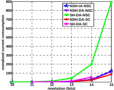
Fig.5 illustrates the optimized total current consumption versus the overall resolution in different conditions. Without the front-end S/H, the minimum capacitance used here already satisfies the noise requirements for 10-12 bits. On the other hand the required capacitance is larger than the acceptable value for 15 bits with the front-end S/H. Thus the capacitor scaling is not done in such cases. It can be observed that the increasing rates of the current consumption are varied in the five optimization conditions, which means that the influence levels of the factors discussed in the optimization considerations are quite different. The effect of stage accuracy scaling down becomes insignificant with the increasing of resolution. As Fig.5 demonstrates, capacitor scaling is necessary when the front-end S/H is used; otherwise power consumption is increased sharply especially in high resolution cases. A comparison of the effects of different factors on power reducing is given in TABLE II.
[image:5.595.70.262.465.617.2]Fig.5 The optimized total current consumption versus the overall resolution in five optimization conditions
TABLE II
Power reducing percentage of different factors
Factor Percentage
Stage accuracy 8%-20%
Capacitor scaling without S/H 18%-26% Capacitor scaling with S/H 46%-78%
The optimum configuration is varied with the optimization conditions. TABLE III gives the optimum
configurations of 14 bits in five optimization conditions. From the power consumption point of view, it’s desirable that increasing the resolutions of the first and the last stages while resolving 2 bits in other stages. Fig.6 gives a comparison of the stage current between the optimized and the traditional 1.5-bit/stage configurations of 14 bits in the optimization conditions of NSH_DA_SC and SH_DA _SC (with one overlapping bit, the effective resolution of 2-bit/satage is 1.5-bit/stage.). As it shows, if the resolution of the first stage is properly chosen, the power consumption of the following stages can be reduced greatly while only a little power may be increased in the first stage. On the other hand, the number of stages will decrease by resolving more bits in the last stage which adds little load capacitances to the proceeding stage, thus the total power is reduced. The result is supported by [14], which accords with the general architecture described in this paper. It also can be observed that the current consumption is dominated by the front stages. Fig.7 shows the comparison of the stage unit capacitance corresponding to Fig.6. As seen from Fig.6-7, the front-end input S/H introduces considerable power and area in the front stages. Fig.7 shows that the capacitor scaling is stopped when the minimum capacitance is reached. It can be seen that the capacitor sizes are greatly reduced in the optimized configurations compared with the traditional ones.
To illustrate the effect of resolution distribution on power optimization, Fig.8 gives a comparison of the total current consumption of some representative configurations of 14 bits in the optimization conditions of NSH_DA_SC. It can be seen that the configuration of 4-2-2-2-2-2-2-2-2-3 consumes the minimum power.
TABLE III
The optimum configurations of 14 bits in five optimization conditions (with one overlapping bit)
Optimization conditions Optimum configuration
NSH_IA_NSC [5 2 2 2 2 2 5 ]
NSH_DA_NSC [4 2 2 2 2 2 2 5]
NSH_DA_SC [4 2 2 2 2 2 2 2 2 3]
SH_DA_NSC [3 2 2 2 2 2 2 2 5]
[image:5.595.309.543.472.740.2]SH_DA_SC [4 2 2 2 2 2 2 2 2 3]
Fig.6 Comparison of bias current of RA between the optimized and 1.5-bit/stage configurations of 14 bits (in
NSH_DA_SC and SH_DA _SC)
10 11 12 13 14 15 0
100 200 300 400 500 600 700 800 900
resolution (bits)
n
o
m
al
iz
ed
cu
rr
e
n
t co
m
s
u
m
p
ti
o
n
NSH-IA-NSC NSH-DA-NSC SH-DA-NSC NSH-DA-SC SH-DA-SC
0 1 2 3 4 5 6 7 8 9 10 11 12 0
10 20 30 40 50 60
stage number( 0 reprents the front-end SH )
b
ias
cu
rr
e
n
t o
f R
A
(
m
A
)
Fig.7 Comparison of stage unit capacitance between the optimized and 1.5-bit/stage configurations of 14 bits (in
NSH_DA_SC and SH_DA _SC)
Fig.8 Total current consumption comparison of different configurations of 14-bit pipeline ADC in NSH_DA_SC
VI. CONCLUSIONS
By analyzing the power sources and optimization considerations of a switched-capacitor pipeline ADC, an optimization methodology is proposed for the systematic automation design. The main factors related to reducing power are investigated using a developed CAD tool, in which optimization is constrained by the input parameters dependent on the specification and manufacture process of the ADC. 10 to 15-bit ADCs are explored to get some instructive design rules and the optimization results of a 14-bit, 100MS/s pipeline ADC are shown in detail.
ACKNOWLEDGMENT
This paper is sponsored by the National Natural Science Foundation of China under grant No. 60906012. It also gains support from the Analog Devices, Inc. (ADI). The authors would like to thank Mr. Bill Liu, the senior engineers of ADI and his colleagues, for their useful discussions and instruction.
REFERENCE
[1] S. H. Lewis, “Optimizing the stage resolution in pipelined, multistage, analog-to-digital converters for video-rate applications”, IEEE transactions on circuits and systems II: Analog and digital signal processing, Vol. 39, No.8, Aug.1992, pp. 516-523.
[2] D. W. Cline, P. R. Gray, “A Power Optimized 13-b 5Msamples/s
Pipelined Analog-to-Digital Converter in 1.2µm CMOS”, IEEE Journal of Solid-State Circuits, Vol. 31, No. 3, Mar. 1996, pp. 294-303. [3] J. Goes, J. C. Vital, J. E. Franca, “Systematic Design for Optimization of High-Speed Self-Calibrated Pipelined A/D Converters”, IEEE transactions on circuits and systems II: Analog and digital signal processing, Vol. 45, No. 12, Dec.1998, pp. 1513-1526.
[4] M. Hershenson, "Design of pipeline analog-to-digital converters via geometric programming," in Proc. of IEEE Intl. Conf on Computer Aided Design, 2002, pp. 317-324.
[5] Reza Lotfi, Mohammad Taherzadeh-Sani, M Yaser Azizi and Omid Shoaei, “Systematic Design for Power Minimization of Pipelined Analog-to-Digital Converters”, in Proc. Of International Conference on Computer Aided Design (ICCAD), 2003, pp. 371-374.
[6] Chang-Hyuk Cho, A Power optimized pipelined analog-to-digital converter design in deep sub-micro CMOS technology, Ph.D thesis, Georgia Institute of Technology, 2005.
[7] Yun Chiu, P. R. Gray, “A 14-b 12-Ms/s CMOS Pipeline ADC with over 100-dB SFDR”, IEEE Journal of Solid-State Circuits, Vol. 39, No. 12, Dec. 2004, pp.2139-2151.
[8] S. H. Lewis, “10-b 20-Msample/s analog-to-digital converter”, IEEE Journal of Solid-state Circuits, Vol. 27, No.3, March 1992, pp.351-358.
[9] Dong-Young Chang, “Design Techniques for a Pipelined ADC without Using a Front-End Sample-and-Hold Amplifier”, IEEE transactions on circuits and systems I: regular papers, Vol. 51, No. 11, Nov.2004, pp. 2123-2132.
[10] Cao Junmin, Chen Zhongjian, Lu Wengao and Zhao Baoying, “A Low Power 12-Bit 20Msamples/s Pipelined ADC”, International Conference on Signal Processing Systems (ICSPS), 2009, pp. 77-80. [11] T. Cho, Low-power Low-voltage, Analog-to-Digital Conversion
Technique using pipelined architectures, Ph.D thesis, University of California, Berkeley, 1995.
[12] N. Paulino, J. Goes and A. Steiger-Garcao, “Design Methodology for Optimization of Analogue Building-Blocks using Genetic Algorithms”, IEEE ISCAS’2001, 2001, pp.435-438.
[13] B. Vaz et al, “A General-purpose Kernel based on Genetic Algorithms for Optimization of Complex analog circuits”, Proc. IEEE MWSCAS’2001, 2001, pp.83-86.
[14] Wenhua Yang, Dan Kelly, Iuri Mehr, Mark T. Sayuk and Larry Singer, “A 3-V 340-mW 14-b 75-Msample/s CMOS ADC With 85-dB SFDR”, IEEE Journal of Solid-State Circuits, Vol. 36, No.12, Dec. 2001, pp. 1931-1936.
0 1 2 3 4 5 6 7 8 9 10 11 12 0
5 10 15 20 25
stage number( 0 reprents the front-end SH )
u
n
it
cap
aci
ta
n
c
e
(
p
F
)
22222222222222(NSH-DA-SC) 22222222222222(SH-DA-SC) 4222222223(SH-DA-SC) 4222222223(NSH-DA-SC)
1 2 3 4 5 6 7 8 9 10 0
10 20 30 40 50 60 70
configuration number
c
u
rr
e
nt
c
o
n
s
um
pt
ion (
m
A)
222...22
3322...223
322...223
4322...22
422...223 522...22
333222223 43322...22
322...222