Amirkabir University of Technology (Tehran Polytechnic)
Vol. 47, No. 1, Spring 2015, pp. 31- 37
Amirkabir International Journal of Science& Research (Electrical & Electronics Engineering)
AIJ-EEE) )
٭
Corresponding Author, Email: [email protected]
Vol. 47, No. 1, Spring 2015 31
A Class E Power Amplifier with Low Voltage Stress
M. Hayati
1*and S. Roshani
21- Professor, Department of Electrical Engineering, Faculty of Engineering, Razi University, Tagh-E-Bostan, Kermanshah-67149, Iran
2- Faculty Member, Department of Electrical Engineering, Kermanshah Branch, Islamic Azad University, Kermanshah, Iran
ABSTRACT
A new output structure for class E power amplifier (PA) is proposed in this paper. A series LC resonator
circuit, tuned near the second harmonic of the operating frequency is added to the output circuit. This
resonator causes low impedance at the second harmonic. The output circuit is designed to shape the switch
voltage of the class E amplifier and lower the voltage stress of the transistor. The maximum switch voltage
of the conventional class E PA is 3.56Vdc. However, higher switch voltage of about 4.5V
DCmay be
occurred, by considering nonlinear drain-to-source capacitance in class E PA. The obtained peak switch
voltage of the designed class E PA is approximately 75% of the conventional one with the same conditions,
which shows a significant reduction in peak switch voltage. MOSFET parasitic nonlinear gate-to-drain and
nonlinear drain-to-source capacitances of the MOSFET body junction diode also affect the switch voltage in
class E PA, which are considered in this paper. The actual MOSFETs have these parasitic capacitances;
therefore, it is necessary to consider these elements in the design procedure. Reduced switch voltage in class
E PA relaxes the breakdown voltage constraints of the active device. In the switch voltage of the designed
circuit, the zero voltage and zero derivative switching (ZVS and ZVDS) conditions are satisfied. Simulation
of the presented circuit is performed using PSpice and LTspice softwares. For verification of the designed
circuit, the presented PA is fabricated and measured.
KEYWORDS
1- INTRODUCTION
Power amplifiers are high power-consuming elements in any communication system, so efficiency is a very important factor in the design process [1-2]. High efficiency power amplifiers have become one of the most significant components in the modern communication [3-4]. Switching mode power amplifiers are very high-efficiency amplifiers among the different classes of operations. One of the most important switching mode power amplifiers is class E PA, which is being used in power electronics and radio-frequency applications [5-6]. The class E PA was introduced in 1975 [7], which becomes popular due to high conversion efficiency and good performance in high frequencies. ZVS and ZVDS conditions in class E PA guarantee the switching loss, low noise and high efficiency at high frequencies [8]. The efficiency of the class E PA can approach 100 percent theoretically, due to its shape of the switch voltage and current waveforms which has no overlap in the time domain. Maximum switch voltage in conventional class E power amplifier is 3.56VDC [7]. Several parameters can
change the voltage stress in class E PA, for instance, the nonlinearity of drain-to-source MOSFET capacitance can increase the maximum switch voltage to about 4.5VDC
[9-16]. Hence, adding linear shunt capacitance in parallel with the drain-to-source capacitance will lower the maximum switch voltage of the class E power amplifier [13]. However, this method cannot reduce the voltage stress lower than 3.56VDC. The duty ratio can also affect
the maximum switch voltage of the amplifier [14-15]. Increasing the duty ratio can reduce the maximum switch voltage of the class E amplifier. The peak switch voltage also depends on the DC supply voltage and the MOSFET type [16].
In practice, high maximum switch voltage is a limitation for designing the class E power amplifier. The peak switch voltage cannot exceed a significant value because of breakdown drain-to-source voltage of the MOSFET, which limits the output power of the PA. Besides, the high peak switch voltage results in a lower power output capability, considering constant peak switch current.
According to the mentioned disadvantages of high peak switch voltage, several methods have been presented to decrease this value. Zener diodes [17] or transformer with diode [18] are used in class E PA to reduce the peak switch voltage; however, a loss is occurred in the Zener diode. Inverse class E [19-20] and the E/F [21-22] family amplifiers have been introduced which lower the pick switch voltage, compared with the conventional class E PA.
The structure of inverse class E amplifier is symmetrical with class E PA, which can achieve 100 percent drain efficiency with zero current switching (ZCS) and zero current derivative switching (ZCDS) conditions under 50% duty ratio [23-24]. The Inverse class E peak switch voltage is approximately 20% lower than that of class E amplifier, which is 2.86VDC .
The E/F family amplifiers use control harmonic elements with class E amplifier structure. These amplifiers have been presented with reduced switch voltage compared to the conventional class E. However, the class E/F efficiency is lower compared to the class E PA. The ZVS and ZVDS conditions can also be satisfied in these amplifiers [22].
Sub-nominal class E amplifier can operate with lower peak switch voltage [25-26]. The class E power amplifier, which satisfies only the ZVS condition, is called the class E at sub-nominal condition, while the nominal condition requires both the ZVS and ZVDS conditions [20].A flat top switch voltage class E PA is presented in [27] with 19% reduction in the maximum switch voltage. A parallel resonator tuned at second harmonic is added in the output path, after the conventional series resonator. More output power capability is achieved in this research; however, the output voltage waveform is not pure sinusoidal waveform.
A push-pull structure for class E power amplifier with a pair of LC resonant networks is designed in [28] with reduced peak switch voltage. Likewise, current mode class D amplifier has been introduced [29-30] with a lower switch voltage; however, current mode class D only achieves ZVS condition.
Reduced switch voltage leads to the lower transistor peak voltage, compared with the conventional class E. Hence, according to the reduced stress, more output power can be achieved with the same amount of stress [27]. Lower peak switch voltage also decreases the risk of the device failure due to the transistor breakdown mechanism and therefore, relaxes the breakdown voltage constraints of the active device [19].
Vol. 47, No. 1, Spring 2015 33
2-CONVENTIONALCLASSEPOWER
AMPLIFIER
TheStructure of conventional class E power amplifier is shown in Fig. 1. As can be seen from the figure, conventional class E PA consists of DC supply voltage (VDC), a power MOSFET as a switching device, series
resonant circuit (L0 - C0), shifting inductor (Ls), shunt
capacitance, DC-feed inductance (LRFC) and the load
resistance (R). The shunt capacitance includes MOSFET intrinsic nonlinear drain-to-source capacitance (Cds) and
an external linear shunt capacitance (Cex). In this paper,
both Cex and Cds are considered in class E PA. The
inductance Ls shifts the phase of the output current, while
the resonant inductor L0 with resonant capacitance C0
form an series LC circuit to resonant in the operating frequency [16].
Cex VDC
LRFC
L
R vo
L0 s
vin
C0
Cds
Fig. 1. Equivalent circuit of conventional class E power amplifier
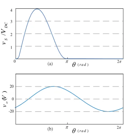
Fig. 2 shows the simulated normalized switch voltage and output voltage waveforms of the conventional class E power amplifier circuit. As can be seen from Fig. 2, the peak switch voltage is 4VDC in the simulated waveforms.
This is because of the nonlinear drain-to-source capacitance which is in the MOSFET PSpice model. However, the external linear capacitance reduces the peak switch voltage. In other words, if the external capacitance is not considered in the circuit, the maximum switch voltage of the class E PA will be increased to about 4.5VDC.
3-STRUCTUREOFTHEPRESENTEDCLASSE
AMPLIFIER
Fig. 3 shows the structure of the presented class E amplifier. In the presented structure, a series LC resonator circuit, tuned near the second harmonic of the operating frequency is added between the shifting inductance and series inductance. This series resonator makes a zero near the second harmonic of the operating frequency.
0
2/
S
D
C
vV
(r a d)
()
o
vV
0 1
-20
2
2 3 4
(a)
(b)
20
(r a d)Fig. 2. Simulated waveforms of (a) normalized switch voltage and (b) output voltage for conventional class E power amplifier
Cex VDC
LRFC
L
R
v
L0 s
vin
C0
Cds C2
L2
v
vs LC o
ZLC ZD
Fig. 3. Structure of the presented class E amplifier
The presented circuit is designed in such way that the impedance seen from drain will be low at first and second harmonics, while it will be large at the third harmonic. In other words, the load structure should make a pole at the third harmonic and two zeros at first and second harmonics. Therefore, the second harmonic is eliminated from the switch voltage and the third harmonic will be added to it. Consequently, the peak switch voltage will be reduced. The impedance of the output network, seen by the drain, when the switch is off, is shown in Fig. 4. However, the ZVS and ZVDS conditions can be satisfied, which result in high efficiency and zero switching loss at high frequencies in the designed class E PA.
34 Vol. 47, No. 1, Spring 015 shorted and allows the fundamental component of the
switch voltage to pass. The series L2C2 resonator will be
shorted near the second harmonic, so the drain sees low impedance at this frequency. At the third harmonic, the drain sees the same lumped elements, but with different values, which cause high impedance. The series L0C0
resonant circuit is opened at second and third harmonics, so the resistant R will not seen by drain in these harmonics.
1.0 1.5 2.0 2.5 3.0 3.5
0.5 4.0 0 20 40 60 80 -20 100 0
f 2f0 3f0 4f0
Frequency (MHz) M a g n it u d e ( d B Ω )
Fig. 4. Impedance of the output network seen by the drain, when the switch is off
L
R
L C Csh
Csh R
L
R
Csh Open
L
R
Csh Short
class E
0
2f
03f
0class E/F2
class E/F3
proposed PA
PA type
f
s s s s 2 L2 L C Csh s 2 L2 L C Csh s 2 L2Fig. 5. Structures of different switching PAs versus harmonics
1.0 1.5 2.0 2.5 3.0 3.5
0.5 4.0
Frequency (MHz)
LS = 2 μH
LS = 3 μH
LS= 4 μH
LS = 5 μH
LS = 6 μH
LS = 1 μH
0 20 40 60 80 -20 100 M ag n it u d e (d B Ω ) 120
Cex = 270 pF
Cex = 370 pF
Cex = 470 pF
Cex = 570 pF
Cex = 670 pF
Cex = 770 pF
1.0 1.5 2.0 2.5 3.0 3.5
0.5 4.0 Frequency (MHz) 0 20 40 60 80 -20 100 M ag n it u d e (d B Ω ) 120
(a)
(b)
Fig. 6. The effects of (a) Ls and (b) Cex on drain impedance
4- DESIGN PROCEDURE OF PRESENTED STRUCTURE
According to Fig. 3, the series resonant circuit, L0C0,
should be shorted at the operating frequency, which is
f0=1 MHz. The value of L0 can be obtained using the
following equation: 0 0 RQ L (a) R Cds R Cgs Cgd s g
10 20 30 40 50
1 0.2 0.6 1 1.4 Cgs Cds Cgd ( ) C nF (c) ( ) ds V V (b)
Fig. 7. (a) Simplified MOSFET model. (b) Fabricated circuit of the presented class E PA. (c) MOSFET parasitic gate-to-source, gate-to-drain and drain-to-source capacitances(1)
TABLE 1. PARAMETERS OF IRF530 AND IRFF510 MOSFETS
Cj0 Cgd Cgs Vbi Vth
IRF530 1151 pF 177.75 pF 596.15pF 0.8 V 3.2 V
Vol. 47, No. 1, Spring 2015 35 where Q is the loaded quality factor of the output
resonant circuit. High value of Q is needed, due to the pure sinusoidal output waveform. The operating frequency can be written as
(2)
0
0 0
1
L C
From (1) and (2), the value of C0 can be achieved. The
resonant circuit of L2C2 should make a zero at near the
second harmonic, according to Fig. 4. Appropriate values of L2 andC2are selected to provide low drain impedance
near the second harmonic. The drain impedance can be written as:
(3)
2
,
1
LC SD
S ex LC ex
Z
L S
Z
L C S
Z
C S
where ZLCis the impedance of vLC node, as shown in Fig.
3. ZLC is defined as follows:
(4)
4 3 2
2 0 2 0 2 2 0 2 2 0 0 0
3 2
2 0 2 0 2 0 2 0
1
LC
Z
L L C C S RL C C S L C L C S RC S
L L C C S RC C S C C S
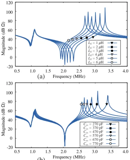
Fig. 6 shows the drain impedance, which is obtained using (3) and (4). The effects of Ls and Cex on drain
impedance are also shown in Fig. 6. According to this figure, Ls changes the locations of zero and pole at second
and third harmonics, respectively, while Cex changes only
the third harmonic pole location. Therefore, the values of
Ls and Cex should be selected according to the desired
zero and pole locations, which are chosen 4 μH and 470 pF, respectively. The values of the obtained circuit elements are shown in Table 2.
5-SIMULATIONANDEXPERIMENTALRESULTS
MOSFET IRF530 is selected as a switching device in the designed amplifier. Parameters of IRF530 and IRF510 MOSFETs are extracted according to datasheet, which are given in Table 1. In fact, the actual MOSFETs have several parasitic components which should be considered in the design procedure. The simplified MOSFET model, which is used in this paper and the fabricated circuit of the presented class E PA, are shown in Figs. 7(a) and (b), respectively. The nonlinear drain-to-source capacitance is considered in PSpice MOSFET model, while the gate-to-source and gate-to-drain capacitance is considered to be linear. However, in LTspice MOSFET model, the drain-to-source and to-drain capacitances are assumed nonlinear and the gate-to-source capacitance is considered linear. The calculated parasitic capacitances of MOSFET IRF530 are shown in Fig. 7(c), according to its datasheet information. As can be seen in this figure, the gate-to-source capacitance is
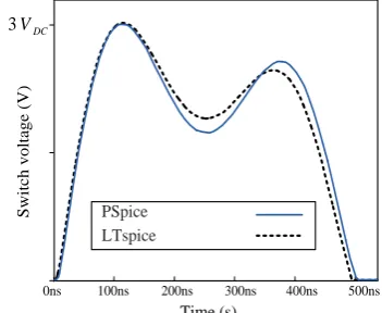
approximately linear, while the drain-to-source and gate-to-drain capacitance are highly nonlinear, which affect the design specifications. The simulation results of switch voltage for designed amplifier, using PSpice and LTspice softwares are shown in Fig. 8. According to this figure, the maximum switch voltage of the designed amplifier is 3VDC which is equal to 60 V. A significant reduction in
switch voltage with the same output power has been achieved, compared with the conventional class E power amplifier peak switch voltage, which is shown in Fig. 2(a). The circuit is designed at the operating frequency f0
= 1 MHz, duty cycle 0.5 and output power of 8.3 W.The values of the design specifications and obtained results for the proposed circuit are given in Table 2. The experimental and simulated waveforms of switch voltage (vs) and output voltage (vo) for the presented class E
power amplifier are shown in Fig. 9. The simulation waveforms are obtained, using PSpice software. According to Fig. 9, the designed class E PA works in the nominal condition. The experimental and the simulated results are in good agreement.
6-CONCLUSION
A new structure for class E power amplifier was designed and fabricated. About 25% reduction of peak switch voltage was achieved, compared to the conventional class E power amplifier. The nominal operating conditions were achieved in the proposed structure, namely ZVS and ZVDS were satisfied. With the reduced peak switch voltage, higher output power can be achieved in class E power amplifier. The nonlinearity of drain-to-source and gate-to-drain MOSFET parasitic capacitances were considered in the design of presented amplifier. The simulations were performed using PSpice and LTspice softwares. A good agreement was observed between the experimental and the simulated results of the fabricated power amplifier
S
w
it
c
h
v
o
lt
a
g
e
(
V
)
PSpice LTspice
0ns 100ns 200ns 300ns 400ns 500ns V(n002)
3VDC
Time (s)
0
2
(rad)0 10 20 30 40 50 60
-10
-20
S
w
it
c
h
a
n
d
o
u
tp
u
t
v
o
lt
a
g
e
s
(V
)
0
2
(rad)0 10 20 30 40 50 60
-10
-20
S
w
it
c
h
a
n
d
o
u
tp
u
t
v
o
lt
a
g
e
s
(V
)
(a)
(b)
S v
o
v
Fig. 9. (a) PSpice simulation and (b) experimental waveforms of the proposed class E power amplifier
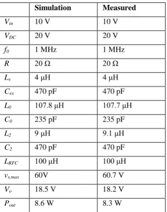
TABLE 2. EXPERIMENTAL AND PSPICE SIMULATION RESULTS OF DESIGNED PA
Simulation Measured
Vin 10 V 10 V
VDC 20 V 20 V
f0 1 MHz 1 MHz
R 20 Ω 20 Ω
Ls 4 μH 4 μH
Cex 470 pF 470 pF
L0 107.8 μH 107.7 μH
C0 235 pF 235 pF
L2 9 μH 9.1 μH
C2 470 pF 470 pF
LRFC 100 μH 100 μH
vs,max 60V 60.7 V
Vo 18.5 V 18.2 V
Pout 8.6 W 8.3 W
REFERENCES
[1] H. Golestaneh, A. Abdipour, and A. Mohammadi, “Nonlinear modeling and analysis of a Doherty power amplifier driven by non-constant envelope signals”, Analog Integrated Circuits and Signal Processing, vol. 72, No. 1, pp. 141-153. 2012.
[2] M. Majidi, A. Mohammadi, and A. Abdipour, “Analysis of the power amplifier nonlinearity on the power allocation in cognitive radio networks”, IEEE Transactions on Communications, vol. 62, No. 2, pp. 467-477, 2014.
[3] M. Hayati, F. Shamma, S. Roshani, and A. Abdipour, “Linearization design method in class-F power amplifier using artificial neural network.” Journal of Computational Electronics, vol. 13, No. 4, pp. 943-949, 2014. [4] M. Hayati and S. Roshani, “A novel
miniaturized power amplifier with nth harmonic suppression”, AEU-International Journal of Electronics and Communications, vol. 68, No. 10, pp. 1016-1021, 2014.
[5] M. Vasic, O. Garcia, J. A. Oliver, P. Alou, D. Diaz, R. Prieto, and J. Cobos, “Envelope amplifier based on switching capacitors for high-efficiency RF amplifiers”, Power Electronics, IEEE Transactions on, vol. 27, No. 3, pp. 1359-1368, 2012.
[6] A. Mediano and N. O. Sokal, “A Class-RF Power Amplifier with a Flat-Top Transistor-Voltage Waveform”, IEEE Transactions on Power Electronics, vol. 28, No. 11, pp. 5215-5221, 2013.
[7] N. O. Sokal and A.D. Sokal, “Class EA new class of high-efficiency tuned single-ended switching power amplifiers”, IEEE Journal of Solid-State Circuits, vol. 10, No. 3, pp. 168-176, 1975.
[8] M. K. Kazimierczuk, RF Power Amplifier, John Wiley & Sons, 2014.
[9] M. J. Chudobiak, “The use of parasitic nonlinear capacitors in class E amplifiers”, IEEE Transactions on Circuits and Systems I: Fundamental Theory and Applications, vol. 41, No. 12, pp. 941-944, 1994.
[10] T. Suetsugu and M. K. Kazimierczuk, “Comparison of class-E amplifier with nonlinear and linear shunt capacitance”, IEEE Transactions on Circuits and Systems I: Fundamental Theory and Applications, vol. 50, No. 8, pp. 1089-1097, 2003.
Vol. 47, No. 1, Spring 2015 37 class E power amplifier with nonlinear
parasitic output capacitance”, IEEE Transactions on Circuits and Systems II: Analog and Digital Signal Processing, vol. 46, No. 2, pp. 114-119, 1999.
[13] T. Suetsugu and M. K. Kazimierczuk, “Analysis and design of class E amplifier with shunt capacitance composed of nonlinear and linear capacitances”, IEEE Transactions on Circuits and Systems I: Regular Papers, vol. 51, No. 7, pp. 1261-1268, 2004.
[14] T. Suetsugu and M. K. Kazimierczuk, “Maximum operating frequency of class-E amplifier at any duty ratio”, IEEE Transactions on Circuits and Systems II: Express Briefs, vol. 8, No. 55, pp. 768-770, 2008.
[15] M. Hayati, A. Lotfi, M. K. Kazimierczuk, and H. Sekiya, “Analysis and design of class-E power amplifier with MOSFET parasitic linear and nonlinear capacitances at any duty ratio.” IEEE Transactions on Power Electronics, vol. 28, No. 11, pp. 5222-5232. 2013.
[16] X. Wei, H. Sekiya, S. Kuroiwa, T. Suetsugu, and M.K. Kazimierczuk, “Design of class-E amplifier with MOSFET linear gate-to-drain and nonlinear drain-to-source capacitances”, IEEE Transactions on Circuits and Systems I: Regular Papers, vol. 58, No. 10, pp. 2556-2565. 2011.
[17] T. Suetsugu and M. K. Kazimierczuk, “Voltage-clamped class E amplifier with a Zener diode across the switch”, in IEEE International Symposium on Circuits and Systems, ISCAS, pp. IV-361, 2002.
[18] T. Suetsugu and M. K. Kazimierczuk, “Lossless voltage-clamping of a class E amplifier with a transformer and a diode.” in International Symposium on Circuits and Systems, ISCAS, pp. III-276, 2003.
[19] T. Mury, and V. F. Fusco, “Sensitivity characteristics of inverse Class-E power amplifier”, IEEE Transactions on Circuits and Systems I: Regular Papers, vol. 54, No. 4, pp. 768-778, 2007.
[20] P. Chen, and S. He, “Investigation of Inverse Class-E Power Amplifier at Sub-Nominal Condition for Any Duty Ratio.” IEEE Transactions on Circuits and Systems I: Regular Papers, vol. 62, No. 4, pp. 1015-1024. 2015.
[21] Z. Kaczmarczyk, “High efficiency class E, E/F2 and E/F inverters”, IEEE Transactions on Industrial Electronics, vol. 53, pp. 1584–1593, 2006.
[22] A. Grebennikov, “High-efficiency Class E/F lumped and transmission-line power amplifiers”, IEEE Transactions on Microwave Theory and Techniques, vol. 59, No. 6, pp.
1579-1588. 2011.
[23] T. Mury, and V. F. Fusco, “Inverse Class-E amplifier with transmission-line harmonic suppression”, IEEE Transactions on Circuits and Systems I: Regular Papers, vol. 54, No. 7, pp. 1555-1561, 2007.
[24] F. You, S. He, X. Tang, and X. Deng, “The effects of limited drain current and on resistance on the performance of an LDMOS inverse class-E power amplifier”, IEEE Transactions on Microwave Theory and Techniques, vol. 57, No. 2, pp. 336-343, 2009. [25] T. Suetsugu and M. K. Kazimierczuk, “Design
procedure of class-E amplifier for off-nominal operation at 50% duty ratio”, IEEE Transactions on Circuits and Systems I: Regular Papers, vol. 53, No. 7, pp. 1468-1476, 2006.
[26] M. Hayati, A. Lotfi, M. K. Kazimierczuk, and H. Sekiya, “Performance study of class-E power amplifier with a shunt inductor at subnominal condition”, IEEE Transactions on Power Electronics, vol. 28, No. 8, pp. 3834-3844, 2013.
[27] A. Mediano and N. O. Sokal, “A Class-RF Power Amplifier with a Flat-Top Transistor-Voltage Waveform”, IEEE Transactions on Power Electronics, vol. 28, No. 11, pp. 5215-5221, 2013.
[28] F. Y. Chen, J. F. Chen, and R. L. Lin, “Low-harmonic push–pull Class-E power amplifier with a pair of LC resonant networks”, IEEE Transactions on Circuits and Systems I: Regular Papers, vol. 54, No. 3, pp. 579-589, 2007.
[29] H. Kobayashi, J. M. Hinrichs, and P. M. Asbeck, “Current-mode class-D power amplifiers for high-efficiency RF applications”, IEEE Transactions on Microwave Theory and techniques, vol. 49. No. 12, pp. 2480-2485. 2001.