©IJRASET: All Rights are Reserved
879
Implementation of Class-E CMOS Power Amplifier
T. Suganthi1, R. Prabakaran2
1PG Scholar, Department of ECE, Tejaa Shakthi Institute of Technology for Women, Coimbatore, Tamilnadu 2Assistant Professor, Department of ECE, Tejaa Shakthi Institute of Technology for Women, Coimbatore, Tamilnadu
Abstract: power efficiency being an important factor in power amplifiers, it is strictly noted to use amplifiers in various applications. In switched common source class amplifiers, it is usually obtained at the expense of device stress. At the same time, the power loss happens which can be minimized using positive feedback technique. Generally, class-e power amplifier which is operated as a switch is the one that is used in most applications. Practically, class-e amplifiers can achieve very high efficiencies. This is because there is no short-circuited currents that results in efficiency losses. To demonstrate the performance, class-e power amplifiers is designed in cadence virtuoso environment and simulation is carried out in the spectre simulator. Also smithchart is plotted to get forward and reverse gain in the cadence environment.
Keywords: class-e, cmos, power amplifier, cascode, charge acceleration technique(cat)
I. INTRODUCTION
The interest in designing RF power amplifier in CMOS technology is increasing. This is due to the well-being integrating, besides the digital part of the transceiver. Mobile communications need power amplifiers that are efficient which is necessary for conservation of battery’s life. However, wireless communication for portable devices needs 0–30 dBm (1mW–1 W).
Several efforts have successfully demonstrated the possibility of watt-level CMOS PAs [1–3] but a highly efficient and integrated CMOS PA is a difficult challenge. The class-D, -E and F switching mode PA can theoretically achieve 100% efficiency. Class-D is rarely used for GHz-range applications [4]. Class F is complicated and requires large size for integration.
Practically, the class-E amplifier introduced by Sokal [5] has the best performance. The common topology for class-E is single stage common- source, but this topology due to high drain voltage stress is under the peril of oxide breakdown and hot carrier effect in CMOS technology [6]. Catastropic situation is created by proportionality of output power to supply voltage [7, 8]. The cascode topology was first employed to compensate the larger degradations at high supply voltage’s stress level [9]. The non-ideality of cascode topology results in power loss. Even though, it is minimized by using positive feedback technique, this topology shows less efficiency. Thus, the class-E power amplifier is proposed which is designed using cadence shows higher efficiency than the existing. The transient and ac response is taken and the gain and magnitude is noted and efficiency is compared.
A. Design and Simulation of CMOS Class-E
[image:2.612.207.410.578.699.2]To demonstrate the performance of proposed technique CMOS class-E PA with feedback path is designed and simulated and the results are compared with cascode PA. Both power amplifiers are designed in 0.18mm CMOS process. Figure 1 shows the complete schematic of class E PA. The designed PA consists of a driver stage and a power stage. The driver stage is a single common-source class-E work with 1.8V supply voltage. The gate length of driver stage is 0.18mm and its width must be such that it has lower power loss. To have an optimum design, one- tenth of common-source width of power stage has been chosen. The gate source capacitor must be small so as to have better driving and less power dissipation. The width of the gate is chosen as 4320mm to have the optimum operation.
©IJRASET: All Rights are Reserved
[image:3.612.205.416.79.192.2]880
Figure 2: Cascode class-E power amplifierB. Cascode class-e power amplifier
To evaluate the class E PA reliability by experiments, a cascode class E PA is designed for fabrication. Figure 2 shows the circuit schematics of a cascode class E PA. A cascode class-E provides high reliability with respect to breakdown considerations [10]. But it causes a power loss due to the slow transition of a common-gate device from the triode region to the cut-off region. So to minimize the power loss of cascode a charging acceleration technique (CAT) is employed that incorporates a capacitive element between the drain and the source of a common-gate device in a cascode configuration, accelerating the charging speed.
Power losses of PAs are mainly caused by active devices and lossy passive elements. Several studies have addressed power losses in class-E PAs, including power losses due to the loss resistances of devices and passive elements [11]. The gain of the cascode configuration is shown in Figure 4.
[image:3.612.207.411.384.541.2]II. RESULT AND DESCRIPTION
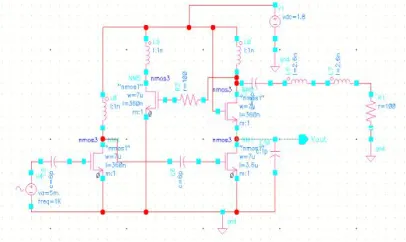
Figure 3 shows the comparison of transient response of cascode and the proposed class E amplifiers. The simulation result shows improvement in efficiency and gain.
[image:3.612.203.410.569.694.2]Figure 3: Transient response of cascode and proposed class E amplifier.
©IJRASET: All Rights are Reserved
881
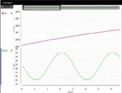
The transient response of the proposed class E amplifier is shown in figure 4. The input voltage of 5mV has got the output of 1.45V. [image:4.612.54.563.377.692.2]Figure 5: Transient response of cascode class E PA.
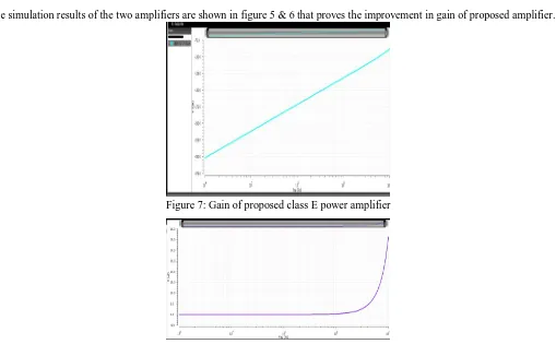
Figure 6: Gain of cascode power amplifier
The simulation results of the two amplifiers are shown in figure 5 & 6 that proves the improvement in gain of proposed amplifier.
Figure 7: Gain of proposed class E power amplifier
©IJRASET: All Rights are Reserved
[image:5.612.206.412.106.428.2]882
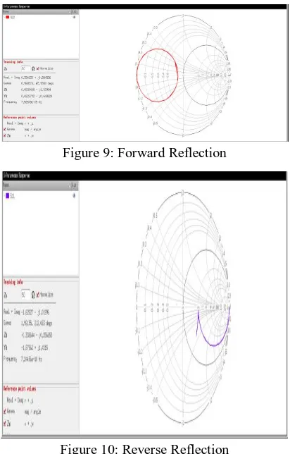
The magnitude response of the class- E power amplifier is shown in figure 7, from which it is known that the proposed amplifier has magnitude of 35µV.Figure 9: Forward Reflection
Figure 10: Reverse Reflection
This is an impedance chart transformed from rectangular Z. Normalized to 100 ohms, the center = R100+J0 or Zo (perfect match). For S11 Forward Reflection (input impedance) and S22 Reverse Reflection (output impedance), get the complex impedance match are shown in figure 9 and 10.
III. CONCLUSION
To demonstrate the overall efficiency improvement and performance, separate architectures of cascode and the proposed class E power amplifier was implemented in Cadence Virtuoso tool and the simulation results were obtained using the spectre simulator. Analysis of both the designs was done and various parameters have been noted, such as the gain, magnitude response and transconductance. The proposed class E CMOS power amplifier shows improvement in gain than the cascode power amplifier. To show the impedance matching, smith chart has been plotted. The simulation results shows increment in overall performance of the proposed technique with respect to the cascode power amplifier.
REFERENCES
[1] I.Aoki, S.D.Kee, D.B.Rutledge, A.Hajimiri, Fully integrated CMOS power amplifier design using the distributed active-transformer architecture, IEEE J. Solid-State Circuits37(3)(2002)371–383 ,March.
[2] K.H.An,O.Lee,H.Kim,D.H.Lee,J.Han,K.S.Yang,Y.Kim,J.J.Chang,W.Woo,C.- H.Lee, H.Kim, J.Laskar, Power - combining transformer techniques for fully integrated CMOS power amplifiers, IEEEJ.Solid-StateCircuits43(5)(2008) 1064–1075,May
[3] O.Lee,K.H.An,H.Kim,D.H.Lee,J.Han,K.S.Yang,C.-H.Lee,H.Kim, J.Laskar, Analysis and design of fully integrated high power parallel-circuit class-E CMOS poweramplifiers, IEEETrans. CircuitsSyst. I57 (2010) 725–734, Mar.
[4] S.D.Kee,I.Aoki,A.Hajimiri,D.Rutledge,The class-E/F family of ZVS switching amplifiers, IEEE Trans.Microw.Theory Tech.51(6)(2003)1677–1690,June. [5] N.O. Sokal, A.D.Sokal, ClassE-a new class of high-efficiency tuned single- ended switching power amplifier, IEEEJ.Solid-StateCircuit10(3)(1975) 168–
176,June.
©IJRASET: All Rights are Reserved
883
[7] T.Suetsugu, M.K.Kazimierczuk, Analysis and design of class E amplifier with shunt capacitance composed of nonlinear and linear capacitances, IEEETrans. Circuits Syst.I:Regul.Pap.51(7)(2004)1261–1268
[8] M.Thian, V.F.Fusco, Analysis and design of class-E3F and transmission- line class-E3F2 power amplifiers, IEEE Trans.Circuits Syst.I:Regul.Pap.58(5) (2011)902–912,May.
[9] F.You,S.He,X.Tang,X.Deng,Highefficiency single-ended class-E/F2 power amplifier with finite dc feed inductor, IEEE Trans.Microw. TheoryTech.58(1) (2010)32–40 ,January.
[10] T.Sowlati,D.M.W.Leenaerts,A 2.4 GHz0.18 μm CMOS self-biased cascode power amplifier, IEEEJ.Solid-StateCircuits38(8)(2003)1318–1324,August [11] J.S.Yuan,H.D.Yen,S.Chen,etal.,Experimental verification of RF stress effect on cascade class-EPA performance and reliability, IEEE Trans. Device Mater.
Reliab.12(2)(2012)369–375,June.
[12] D.J.Kessler,M.K.Kazimierczuk,Power losses and efficiency of class E power amplifier at any duty ratio, IEEE Trans. Circuits Syst.I: Regul Pap.51(9)(2004) 1675–1689,September.
[13] A.Mazzanti,L.Larcher,R.Brama,F.Svelto, Analysis of reliability and power efficiency in cascade class-EPAs, IEEEJ.Solid-StateCircuits41(5)(2006) 1222– 1229,May.