Designing CMOS based Class E Power Amplifier
Madhu1, Dr. Priyanka Anand2 1
Student, 2Asistant Professor, Department of Electronics and Communication Engineering, BPS women university Khanpur kalan, India.
Abstract: Here in this paper the power amplifier and CMOS has been explained. The present researches in sector of power amplifier and CMOS are also discussed here. The proposed work focus on the design and implementation of Class E power amplifier that should be CMOS technology based. The simulation of work is made in MATLAB. The design of circuit has been built of Simulink tool available in MATLAB. The proposed work would play significant role in designing application particular integrated circuits. Multi mode class e radio power amplifier has been using 30 nm CMOS technology with programming. This research has proposed Advanced CMOS RF Power Amplifier Architecture. Research has presented PAE% according to frequency. Comparison chart of Tradition researches where frequency was 5.2 to 13 ghz , 4 to 17 ghz, 6.5 to 13 ghz, 0.1 to 65 ghz,0.2 to 2.5 ghz in proposed research frequency 2.4ghz has been represented. Output power & power gain has been simulated in this section. Multi mode class e radio power amplifier has been using 30 nm CMOS technology with programming. Such system would be suitable for low power fifth generation wireless networks.
Keywords: CMOS, MATLAB, Simulink, Power Amplifier, Class E PA
I. INTRODUCTION
Power amplifier has been considered as last block in transmitter system. It has capability to boost weak signal to needed power level. This requirement came in existence when signal is transferred. Power amplifier has been considered huge signal amplifiers. Voltage of input signal need to be high if there is needed to get a huge signal power on output Power Amplifier are classified in audio power amplifiers & rf power amplifiers refers to the Complementary Metal Oxide Semiconductor. It is popular technology in industry of computer chip design. At present time, this technology has been applied to generate the integrated circuits in several and different applications. The technology makes utilization of both P channel & N channel semiconductor devices.
complementary metal oxide semiconductor power amplifier [16] with high linearity was explained. 2.45 Gega Hertz high frequency complementary metal oxide semiconductor Class-AB power amplifier has been proposed.
It has high linearity & output power for WLAN. Two types of PAs were developed to demonstrate accessiblity of mechanism. The improved power amplifier with 2.4 volt supply voltage is having 22.5 dB of power gain. If there is 5 dBm increase of P1dB than fifteen percent & 5 dB updation of PAE at P1dB & IMD3 occurs.
II. RELATED WORKS
There have been several researches that are representing methods for performance improvement of multi-stacked CMOS millimetre wave power amplifiers. The research work has discussed several researches.
In 2018, Mohammad Hassan Montaseri [1] wrote to denote the improvement in Multi-Stacked CMOS mm-Wave PA. This is related and dependent on negative capacitance. The research work has provided the multi-stacked CMOS millimetre-wave PA. This proposed work is related to the negative capacitance phase detuning. It has been analyzed that it is possible to be generalized to different step detuning methods.
In 2018, Ivan Sejc[2] provide the research work on an architecture of DAC that is related to the RMS Power Detector. This detector is used for RF Applications. In the research work, they proposed a wireless receiver RF PD. This proposed tool will be used for 2.4 GHz as well as 5 GHz WLAN bands. Here the offset compensation and measurement mehod has been proposed. It has been formulated within 65 nm CMOS method.
In 2017 Xianghong Gao [3] researched on three level. In the research work, design with implementation of a three level PA within 65nm CMOS method has provided the research work. With the use of neutralization method the proposed PA can offer a peak power achieves. The PA uses 0.2mm2 chip area with the pads.
In 2016 Eli Schwartz [4], provided the introduction of 20dBm CMOS RF PA. The updated technique to PA architecture in CMOS for 802.11ac is presented here. It has been analyzed that it is able to get -35dB EVM along with output power.
In 2016, Gabor Varga[5] made design of an integrated CMOS. A significant active type of genuine root mean square power detecting device was put into place for the very first time in support of communication frequency demands. For example ti can said that Cognitive Radio. The radio frequency capacity of Power detecting device protects a range of 0.5 Gega Hertz to 3 Gega Hertz along with an effective extent of 50 decibel & a lowest recognizable capacity of fifty ohm. These structures make unlike employment of a fake and different balancing device. Its input impedance is very huge. It makes possible to put them over high impedance and also on fifty ohm lines.
In 2015, Aritra Banerjee [6] described High efficiency multi-mode outphasing RF power amplifier. A multi-channel class-E phase shift radio frequency power amplifing device whose performance was very good is introduced in combination of a idle device. With the help of multi channel power amplifing device the performance at minimum power levels can be incresed. It can be achieved by switching ON & OFF of a specific devision as well as by means of device which will increase the performance. The power amplifing device which has been put forward in this paper was prepared inside a forty five micro meter complementary metal oxide semiconductor methodology.
In 2015, Soroush Dehghani [7] described A four to seventeen Giga Hertz Darlington overlapping high speed environment. In support of high speed related examinationan middle stage inductor as well as series peaking RL circuit are used. An output long wavelength corresponding device is adopted for the purpose of gain maintaince & power consistency at highest frequency. It was represented through the determined consequencies that power amplyfing device which was introduced in this paper , shown a gain of ten decibel on the basis of four to seventeen gigahertz under 2-decibel ripple, & excess capacity in between the range of sixteen to eighteen dBm with power added efficiency better than ten percent & power consumption of three hundred and six mega watt. The chip size is only 0.67 mili meter.
In 2010, H. Wang [8] introduced A CMOS Broadband Power Amplifier with Matching Network. A design methodology is also presented in detail. It has been done to change a canonical band pass network in offered matching system.
In 2010, P. Amplifier [9] they put into place for the very first time a monitoring load for the purpose of power efficiency maximization inside a radio frequency to direct current inverter device. A monitoring load device for radio frequency inverters was explained . A monitoring load is put into place for the very first time in order to make the best use of radio frequency to direct current transformation efficiency because the radio frequency input power to rectifier changes. The device includes two rectifiers with two monitoring circuits.
networks at output, input as well as at interstage. The wideband on-chip transformer has been harnessed lacking of any extra inductive application. Therefore wideband power benefits characteristic could be achieved.
In 2016, H. Wu described [11] Analysis & Design of an Ultra broad band Stacked Power Amplifier in CMOS Technology. The research work has proposed the calculation with the design of a two level stacked powers is also determined here.
In to parasitic of on-chip inductors, 2009 Munir M. El-Desouki et al [17] discussed influence of on chip Interconnections. It has been analyzed over the CMOS radio frequency connected circuits. Achieving power- and area-sufficient fully connected transceivers can be studied as issue faced at the time of designing of high-frequency electronic circuits appropriate with the biomedical apps or WSNs. Power losses connected transistors as well as the interconnections. Such are posed design issues in full integration. It is the connection is of power-efficient CMOS radio-frequency connected to circuits.
In 2009, Niklas Zimmermann [18] made system of an Radio frequency based DAC in 65nm CMOS. It is performed in case of transmitters that are multi standard and multimode. Their research work has proposed a radiofrequency digital-to-analog converter. The RF-DAC makes connection of DAC along with mixer functionality within building block which is single. It has basis for a modulator which is direct-digital vector. Such has been utilized in reconfigurable broadband. Along with this it is applicable in multi standard transmitters in the case of mobile transmission.
In 2008 Sheng-Yi Huang et al [19] was put into place for the very first time a most up to date spurious channel radio frequency batteries inside a 0.13 micro meter complementary metal oxide semiconductor methodlogy" An economical radio frequency battery whose formation takes place inside a latest 0.13 micro meter complementary metal oxide semiconductor methodlogy was bring in to limelight from this work. With the help of normal N-well as well as superficious drain insulation method the efficiency of power can be incresed because this process creates a high resistivity zone. The need of additional covers, expenditure and treatment methods are not required.
In 2008, Francesco Carrara [20] discussed Methodology of RF CMOS Power Amplifier. In this research security of CMOS power amplifiers for load mismatch has been found. Research proposed closed-loop protection circuit. It is rely on new current-mode detection. It is also considering comparison mechanism. Efficient RF efficiency and VSWR ruggedness has been considered at the same time.
In 2006, Huang Min Zh et al [21] An Input circuit for the monitoring of Class F Power amplyfing device stated an input control circuit for pushing an overlapping period of class F radio frequency power amplyfing device in penetrating micron sized complementary metal oxide semiconductor methodology has been presented. The input driver circuit would deliver an improvement to high frequency power amplifier's efficiency by reducing drain current distortion & provide better breakdown voltage protection for transistor. The proposed input driver & class F power amplifier are formed on the basis of Silterra high frequency complementary metal oxide semiconductor 0.18mum technology & simulated using Hspice.
In 2005, Kwyro Lee et al [22] offered semiconductor technology’s impact. Its impact has been analyzed on CMOS RF. Digital circuits for application wirelessly is presented here. Both forward scaling of energetic application inverse scaling of interconnection layer. It is interconnection layers along with effectively thicker whole dielectric and metal layers. It is able to offer helpful scenario applicable in all passive application. Finally, impact of CMOS scaling on several digital circuits has been developed. Here the digital modem blocks are considered. Along with this the digital calibration circuits as well as the switching RF power amplifier are determined.
III. DESIGNS AND IMPLEMENTATION
A. Design of RF power detector
Fig 1 RF Power Detector
B. Design Of CMOS
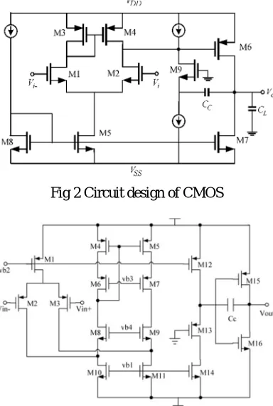
In complementary metal oxide semiconductor methodology, negative-type transistors and positive type transistors has been used for the establishment of reasonable qualties. A particular signal which can start a transistor of one type can be utilized in order to shut down a transistor of different type. Such type of features supports the development of logical gadgets by means of switches in the absence of of a pull-up resistor. In complementary metal oxide semiconductor logic gates an assortment of negative type metal oxide semiconductor field effect transistor are organized inside a pull-down network in the middle of output & low voltage power supply rail (Vss or many times ground).
In comparison to load resistor of negative channel MOS logic gates, complementary metal oxide semiconductor logic gates have an assortment of positive type metal oxide semiconductor field effect transistor inside a pull-up network in the middle of output & higher-voltage rail which is sometimes abbreviated as Vdd.
Therefore in conditions where the gates of negative-type transistors and positive type transistors are connected to identical input, positive type metal oxide semiconductor field effect transistor would start if negative type metal oxide semiconductor field effect transistor is OFF, & vice-versa. The networks are organized in such a way that if one transistor is in ON state , then other will be in OFF state for any input array as illustrated in the diagram below.
[image:4.612.210.402.431.716.2]complementary metal oxide semiconductor offers generally broadband, low power dissipation, high-frequency sound boundries in both states. It has been working within a broad spectrum of source as well as input voltages as long as source voltage is inflexible. In addition to this, for the excellent knowledge of Complementary Metal Oxide Semiconductor operation,a complete explanation related to complementary metal oxide semiconductor logic gates is illustrated below.
Fig 2 Circuit design of CMOS
IV. CALCULATIONS EQUATION
Research has designed of RF power detector for 2.4ghz & 5ghz on 30nm CMOS technique. Doherty principle has been applied. It is used to a 2.5ghz integrated power amplifier over 30nm cmos mechanism.
In proposed work frequency is 2 to 5 (GHz) & PAE% has been simulated accordingly. The following chart is representing PAE% with respect to Frequency. The simulation has been made in MATLAB.
Table 1 the PAE% with respect to Frequency
FREQUENCY(GHz) PAE (%)
0.5 23
1 15
1.5 13
2 12
2.5 8
3 7
3.5 6
4 5.5
4.5 5
5 4.5
frequency=[0.5 1 1.5 2 2.5 3 3.5 4 4.5 5] pae =[23 15 13 12 8 7 6 5.5 5 4.5 4] plot(frequency,pae)
xlabel('Frequency') ylabel('PAE%')
[image:5.612.72.427.115.542.2]title('PAE of power frequency')
Fig 4 Graph plot (Frequency & PAE%)
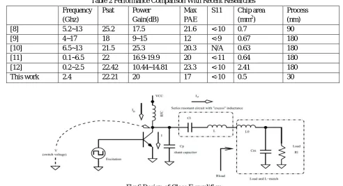
Following chart is representing the optimum load of PA versus frequency here z_opt in case of PAE ROPT , PAE_IOPT, POUT ROPT, POUT_IOPT has been represented.
This chart represent Psat, Power Gain , Max PAE, S11 in dB, Chip area in mm2,process in nm.
Fig 5 Optimum load of PA versus Frequency
[image:5.612.190.432.592.692.2]Table 2 Performance Comparison With Recent Researches Frequency
(Ghz)
Psat Power
Gain(dB)
Max PAE
S11 Chip area
(mm2)
Process (nm)
[8] 5.2~13 25.2 17.5 21.6 <-10 0.7 90
[9] 4~17 18 9~15 12 <-9 0.67 180
[10] 6.5~13 21.5 25.3 20.3 N/A 0.63 180
[11] 0.1~6.5 22 16.9-19.9 20 <-11 0.64 180
[12] 0.2~2.5 22.42 10.44~14.81 23.3 <-10 2.41 180
[image:6.612.58.550.82.349.2]This work 2.4 22.21 20 17 <-10 0.5 30
Fig 6 Design of Class E amplifier
A. Class E amplifier
Class-E conditions are completed at the time when switch closes at
[image:6.612.200.413.514.672.2]The voltage across switch has been provided by V (wt) and present via switch has been represented by I(wt). it has been done at any instant in normalised time wt. For expediency, a table related to variables relavent for analysis has been listed here such as:
Table 1: Table of pertinent variables
B. Design Process
1) Choose power supply voltage (Vdd).
2) It decides Vdd(max) of FET at nearly 3.5 times Vdd
3) Choose target power level
4) It decides optimum value of C1 & optimum load impedance
5) Decide the value of C2 and L2 from Excel Worksheet
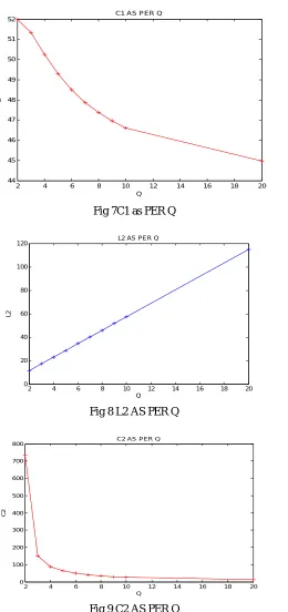
[image:7.612.185.445.178.730.2]C. Matlab Simulation
Fig 7C1 as PER Q
Fig 8 L2 AS PER Q
Fig 9 C2 AS PER Q
2 4 6 8 10 12 14 16 18 20
44 45 46 47 48 49 50 51
52 C1 AS PER Q
Q
C
2 4 6 8 10 12 14 16 18 20
0 20 40 60 80 100
120 L2 AS PER Q
Q
L
2
2 4 6 8 10 12 14 16 18 20
0 100 200 300 400 500 600 700
800 C2 AS PER Q
Q
C
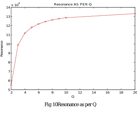
Fig 10Resonance as per Q
V. SCOPE OF RESEARCH
Several areas are there such as Precise RF Power Measurement in Test and as Measurement. Analysis related to Materials with HealthCare are there in which the RF power detectors. The Research work would be beneficial in field of Radar, Electronic Warfare. This research is beneficial where CMOS technology is digital IC designs. It would be useful in field of Computer memories, CPUs, Microprocessor designs, Flash memory chip designing.
The proposed is going to play essential role in designing application specific integrated circuits. Multi mode class E radio power amplifier having 30 nm CMOS technology with programming is proposed. This research has proposed Advanced CMOS radio frequency Power Amplifier Architecture. It has been proposed in case of Low Power 5G Wireless Networks.
VI. CONCLUSION
Research has presented effect of PAE% according to frequency. Tradition researches in which frequency was 5.2 to 13 Ghz , 4 to 17 ghz, 6.5 to 13 Ghz, 0.1 to 65 ghz,0.2 to 2.5 Ghz have been explained & proposed research where frequency 2.4Ghz has been represented. This type of research has been proved significant in wireless communication and CMOS based application. Output power & power gain has been simulated to represent effect of change in frequency & process. It has been observed that influencing factors are Psat, Power Gain, Max PAE when S& frequency is modified.
REFERENCES
[1] M. H. Montaseri, T. Rahkonen, J. Aikio, & A. Pärssinen, “Performance Improvement of Multi-Stacked CMOS mm-Wave Power Amplifiers Based on Negative Capacitance Phase Compensation,” Int. Work. Integr. Nonlinear Microw. Millimetre-Wave Circuits, INMMIC 2018 - Proc., pp. 5–7, 2018.
[2] I. Sejc, S. Popuri, & J. Sturm, “Design of DAC Based RMS Power Detector for RF Applications,” 2018 Austrochip Work. Microelectron., pp. 32–37, 2018. [3] X. Gao, L. Sun, J. Wen, G. Su, M. Jin, & J. Zhou, “A three stage, fully differential D-band CMOS power amplifier,” 2016 13th IEEE Int. Conf. Solid-State
Integr. Circuit Technol. ICSICT 2016 - Proc., pp. 1558–1560, 2017.
[4] E. Schwartz et al., “A 20dBm configurable linear CMOS RF power amplifier for multi-standard transmitters,” Dig. Pap. - IEEE Radio Freq. Integr. Circuits Symp., vol. 2016–July, pp. 318–321, 2016.
[5] G. Varga, B. Wolf, T. Van Rey, A. Ashok, & S. Heinen, “Design of an integrated CMOS highly sensitive true RMS RF power detector for Cognitive Radio applications,” 2016 12th Conf. Ph.D. Res. Microelectron. Electron. PRIME 2016, no. 3, pp. 3–6, 2016.
[6] A. Banerjee, L. Ding, & R. Hezar, “High efficiency multi-mode outphasing RF power amplifier in 45nm CMOS,” Eur. Solid-State Circuits Conf., vol. 2015– October, pp. 168–171, 2015.
[7] S. Dehghani, S. Abbasian, & T. Johnson, “Tracking load to optimize power efficiency in RF to DC rectifier circuits,” 2015 IEEE Wirel. Power Transf. Conf. WPTC 2015, pp. 3–5, 2015.
[8] H. Wang, C. Sideris, & A. Hajimiri, “A CMOS Broadband Power Amplifier With Matching Network,” vol. 45, no. 12, pp. 2709–2722, 2010.
[9] P. Amplifier, C. Technology, P. Huang, K. Lin, & H. Wang, “A 4 – 17 GHz Darlington Cascode Broadband Medium,” vol. 20, no. 1, pp. 2009–2011, 2010. [10] B. Ku, S. Member, S. Baek, & S. Member, “A Wideband Transformer-Coupled CMOS Power,” vol. 59, no. 6, pp. 1599–1609, 2011.
[11] H. Wu, S. Member, Q. Cheng, & S. Member, “Analysis & Design of an Ultrabroadband Stacked Power Amplifier in CMOS Technology,” vol. 63, no. 1, pp. 49–53, 2016.
[12] D. Ren, Z. Ren, K. Zhang, X. Zou, W. Zou, & Y. Yu, “A 0 . 2-2 . 5 GHz CMOS Power Amplifier Using Transformer-Based Broadband Matching Network,” pp. 31–34, 2016.
2 4 6 8 10 12 14 16 18 20
5 6 7 8 9 10 11 12 13 14x 10
4
Resonance AS PER Q
[13] N. Deltimple, M. L. Carneiro, E. Kerhervé, P. H. P. Carvalho, & D. Belot, “Integrated Doherty RF CMOS Power Amplifier design for average efficiency enhancement,” 2015 IEEE Int. Wirel. Symp. IWS 2015, pp. 2–5, 2015.
[14] B. Mohr et al., “An RFDAC based reconfigurable multistandard transmitter in 65 nm CMOS,” Dig. Pap. - IEEE Radio Freq. Integr. Circuits Symp., pp. 109– 112, 2012.
[15] S. Sakphrom & A. Thanachayanont, “201404 Power Detector_References_A low-power CMOS RF power detector,” Electron. Circuits Syst. (ICECS), 2012 19th IEEE Int. Conf., pp. 177–180, 2012.
[16] M. Zhao, L. Sun, J. Wen, Z. Yu, & J. Kang, “A 2.45GHz CMOS power amplifier with high linearity,” ASICON 2009 - Proc. 2009 8th IEEE Int. Conf. ASIC, no. 2, pp. 383–386, 2009.
[17] M. M. El-Desouki, S. M. Abdelsayed, J. M. Deen, N. K. Nikolova, & Y. M. Haddara, “The impact of on-chip interconnections on CMOS RF integrated circuits,” IEEE Trans. Electron Devices, vol. 56, no. 9, pp. 1882–1890, 2009.
[18] N. Zimmermann, R. Negra, & S. Heinen, “Design of an RF-DAC in 65nm CMOS for multistandard, multimode transmitters,” 2009 IEEE Int. Symp. Radio-Frequency Integr. Technol. RFIT 2009, pp. 343–346, 2009.
[19] S. Y. Huang et al., “Novel Pseudo-Drain (PD) RF power cell in 0.13 um CMOS technology,” Dig. Pap. - IEEE Radio Freq. Integr. Circuits Symp., pp. 259– 262, 2008.
[20] F. Carrara, C. D. Presti, A. Scuderi, C. Santagati, & G. Palmisano, “A methodology for fast VSWR protection implemented in a monolithic 3-W 55% PAE RF CMOS power amplifier,” IEEE J. Solid-State Circuits, vol. 43, no. 9, pp. 2057–2066, 2008.
[21] H. M. Zhe, A. K. Bin A’ain, & A. V. Kordesch, “An input driver circuit for class F power amplifier,” 2006 Int. RF Microw. Conf. Proc., pp. 157–159, 2006. [22] K. Lee et al., “The impact of semiconductor technology scaling on CMOS RF & digital circuits for wireless application,” IEEE Trans. Electron Devices, vol.
52, no. 7, pp. 1415–1422, 2005.
[23] N. Zhang et al., “A 60GHz power amplifier using 90-nm RF-CMOS technology,” Proc. Int. Conf. ASIC, pp. 933–936, 2011.
[24] M. A. Khan, D. Kalim, & R. Negra, “Analysis & design of an unconditionally stable common-drain class-B RF power amplifier in 90 nm CMOS technology,” 2011 Work. Integr. Nonlinear Microw. Millimetre-Wave Circuits, INMMiC 2011, no. 1, pp. 4–7, 2011.