ISSN(Online): 2319-8753 ISSN (Print): 2347-6710
I
nternational
J
ournal of
I
nnovative
R
esearch in
S
cience,
E
ngineering and
T
echnology
(A High Impact Factor, Monthly, Peer Reviewed Journal)
Visit: www.ijirset.com
Vol. 8, Issue 11, November 2019
CMOS Implementation of Low Power High
Performance Fast Fourier Transform
Using 180nm Technology
Priyanka Dhayal, Yashika Saini
Research Scholar M.Tech. (VLSI ) , RIET, Jaipur, India
Assistant Professor, RIET, Jaipur, India
ABSTRACT: FFT algorithms are prime models in the design of processing signals. These are widely applied to various WLAN, image processing application, radar and multimedia communication services and spectrum measurements. In this work the design of Decimation in Time-Fast Fourier Transform is described with required improvements in the design as well as in modules used for computation in order to obtain needed low power and low delay results. A low-complexity design for multiplication is essential requirement in Fast Fourier implementation.
I. INTRODUCTION
For digital signal processing systems, the Discrete Fourier Transform (DFT) is the widely used algorithm. These are not calculated directly, but instead are computed with the Fast Fourier Transform (FFT). The computation of N- sample input of this algorithm carries a large number of operations i.e. N2 complex multiplications and N (N−1) complex additions. Since the DFT is based on computation technique, many changes have been proposed for implementing it efficiently and rapidly. It has been continuously applied in Ultra Wide Band (UWB), Radars, receivers and image processing system [3].
Thus a fast algorithm has been made known by Cooley- Turkey, namely Fast Fourier Transform (FFT) by decreasing the number of computing operations. Hence for fast computation of the Discrete Fourier Transform (DFT), the Fast Fourier Transform (FFT) is an efficient and widely accepted technique [1]. This algorithm can be applied in various systems such as fast convolution and correlation, spectrum estimation, signal modulation, etc. With the arrival of semiconductor technologies in VLSI system, FFT design realization need to rise steadily [5].
II. FFT DESCRIPTION
FFT computation is the useful technique to convert the domains i.e the time domain to the frequency domain and the reverse for the implementation on digital hardware is the DFT. For N point DFT of a complex data sequence x(n) is defined in Eq. 1:
X(K)= (1.1)
Where:
ISSN(Online): 2319-8753 ISSN (Print): 2347-6710
I
nternational
J
ournal of
I
nnovative
R
esearch in
S
cience,
E
ngineering and
T
echnology
(A High Impact Factor, Monthly, Peer Reviewed Journal)
Visit: www.ijirset.com
Vol. 8, Issue 11, November 2019
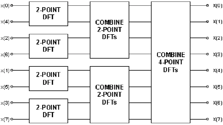
FFT algorithm first divides the system and then calculates i.e it divides the N coefficient points into smaller blocks in different stages. The first stage is implemented with groups of two coefficients, producing N/2 blocks, with each stage calculating the addition and subtraction of the coefficients multiplied by the respective twiddle factors, known as a butterfly. The outputs of these are then used to calculate the next N/4 blocks, which in turn tie up the outputs of two previous blocks, combining four coefficients at this stage. The process is repeated till one main block is produced, with a final calculation of all N coefficients [21].
Figure 1 Computation of an 8-Point DFT in Three Stages using Decimation-In-Time .
III. OBJECTIVE
The main motive of this research is VLSI implementation of FFT architectures, and circuits with the high-performance and energy-efficiency. This includes low power dissipation with high throughput and less propagation delay of the circuit. The main goal of the thesis is as follows:
1. FFT Implementation in 180NM technology.
2. Design of constant Complex multiplier for generation twiddle factor and using Vedic Multiplier for multiplying purpose, which shows various advantages over general multipliers.
3. To design 2 point, 4 point , 8 point FFT butterfly architecture and comparing with already proposed designs with same 180NM technology
Thus with these results and we have tried to make high performance FFT structure with less complexity.
IV. TWIDDLE FACTOR
This is the factor by which the input 2-points are multiplied in the butterfly. The value of N and k depends on the stage of the algorithm as shown in Figure 3.1. They are either stored or calculated on the fly. Some twiddle factors requires no multiplication, but just negation or multiplication by j, like , , , .
ISSN(Online): 2319-8753 ISSN (Print): 2347-6710
I
nternational
J
ournal of
I
nnovative
R
esearch in
S
cience,
E
ngineering and
T
echnology
(A High Impact Factor, Monthly, Peer Reviewed Journal)
Visit: www.ijirset.com
Vol. 8, Issue 11, November 2019
additions reaches a minimum and then increases. Further reductions in computational complexity are possible by simplifying trivial multiplications by ±1 or ±j. With questionable gains, multiplications by π/4, 3π/4, 5π/4, and 7π/4 can also be modified to require fewer actual multiplications [13].
V. CARRY LOOK AHEAD ADDER
The limitations of performance capabilities of RCA are overcome by the carry look-ahead (CLA) adders and improved the speed and performance of the CLA. As the name implies, in carry look-ahead adder all of the inputs are used to improve the addition function and produced carry chain ahead of time. On the bases of inputs, carry signal is calculated in advance which reduces the delay time problem of carry propagation.[12]
Carry look ahead adders addition is a faster way to add two binary numbers to reduce the computation time. In CLA, two signals (P and G) are created for each bit position, based on if a carry is propagated through from a less significant bit position (at least one input is a '1'), a carry is generated in that bit position (both inputs are '1'), or if a carry is killed in that bit position (both inputs are '0'). In maximum cases, the output sum of a half- adder is P signal and carry output of the same adder is G signal. Every bit position carries are created after P and G signal are generated.
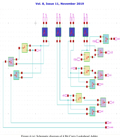
Figure 2: Block Diagrams of 4 Bit Carry Lookahead Adder.
ISSN(Online): 2319-8753 ISSN (Print): 2347-6710
I
nternational
J
ournal of
I
nnovative
R
esearch in
S
cience,
E
ngineering and
T
echnology
(A High Impact Factor, Monthly, Peer Reviewed Journal)
Visit: www.ijirset.com
Vol. 8, Issue 11, November 2019
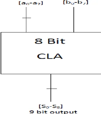
Figure 3: Block Diagrams of 8 Bit Carry Lookahead Adder.
In order to reduce the time to transfer the carry, the carry look-ahead adder is computed by calculating first the carry signals, as per the input signals. Carry Look Ahead adder block diagram of 4 bit input is shown in Fig.2. Fig 3 shows the block diagram of 8 input Carry look ahead adder.
The Boolean expression is manipulated according with full adder in order to understand how the CLA works. The both signals will be valid after one gate delay and propagate and generate signals depend only on the input bits. The Propagate P and generate G in a full-adder, is given as:
Carry propagate (1)
Carry generate (2)
The output carry and sum expression is given by:
(3)
(4)
The general expression of carry signal is
(5)
The above expression clears that the output carry will compute without waiting for the previous carry. Taking an example of 4-bit adder as shown in figure 4.11 and apply these equations to it, the output carries C1, C2, C3 and C4 (last Stage Carry) will be compute as:
ISSN(Online): 2319-8753 ISSN (Print): 2347-6710
I
nternational
J
ournal of
I
nnovative
R
esearch in
S
cience,
E
ngineering and
T
echnology
(A High Impact Factor, Monthly, Peer Reviewed Journal)
Visit: www.ijirset.com
Vol. 8, Issue 11, November 2019
ISSN(Online): 2319-8753 ISSN (Print): 2347-6710
I
nternational
J
ournal of
I
nnovative
R
esearch in
S
cience,
E
ngineering and
T
echnology
(A High Impact Factor, Monthly, Peer Reviewed Journal)
Visit: www.ijirset.com
Vol. 8, Issue 11, November 2019
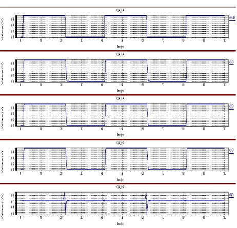
Figure 5(b): Output waveform of 4 bit Carry Lookahead Adder
According to above fig the 4 bit Carry Look Ahead Adder Schematic contains four half adders and various AND, OR, and XOR logic operations. The 5 bit output is produced after the simulation process. The 8 input carry look ahead adder schematic diagram is shown in fig 4(a) with its output waveform resulted from T spice simulation is given in fig 5(b).
ISSN(Online): 2319-8753 ISSN (Print): 2347-6710
I
nternational
J
ournal of
I
nnovative
R
esearch in
S
cience,
E
ngineering and
T
echnology
(A High Impact Factor, Monthly, Peer Reviewed Journal)
Visit: www.ijirset.com
Vol. 8, Issue 11, November 2019
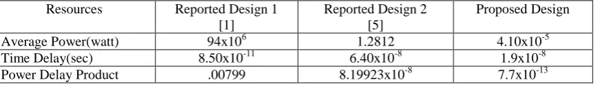
Table 6.1: Result Analysis
Resources Reported Design 1 [1]
Reported Design 2 [5]
Proposed Design
Average Power(watt) 94x106 1.2812 4.10x10⁻⁵
Time Delay(sec) 8.50x10⁻¹¹ 6.40x10⁻⁸ 1.9x10⁻⁸
Power Delay Product .00799 8.19923x10⁻⁸ 7.7x10⁻¹³
VI. CONCLUSION
Simulation results shows that the proposed Fast Fourier transform architecture represents a better and efficient architecture with lesser number of multiplications. This work proposes complex multiplier with reduced number of multipliers which in turn reduces the complexity of the overall design. Also a Constant complex multiplier is designed using adding and shifting operations for twiddle factor generation and multiplication required in Fast Fourier Transform algorithm. This multiplier increases the speed of the FFT designs and contributes to ROM less twiddle factor generators.
The Proposed 8 point Fast Fourier transform architecture is implemented on 180NM CMOS technology library files using tanner Tool. As Low power systems are of great need in current scenario, the T spice simulation results shows that the proposed FFT design offers low power and less delay as compared to reported literature [1] and [5], where total power obtained is 94MW. This is basically due to simplification of the mathematic algorithm in Multiplier operations, which provides the better computation of FFT Architecture.
REFERENCES
[1] Dora Suarez, Renato J. Cintra, F´abio M. Bayer, Arindam Sengupta, Sunera Kulasekera, Arjuna Madanayake, “Multi-Beam RF Aperture Using Multiplierless FFT Approximation”, electronic journal, volume 50,issue 24,2014/DOI-10.1049/el.2014.3561.
[2] Naman Govil,Shubhajit Roy Chowdhury “High Performance and Low Cost Implementation of Fast Fourier Transform Algorithm based on Hardware Software Co-design” , IEEE Region 2014
[3] Deepa Susan George & V.Sarada, “Low Power ROM less FFT Processor” ISSN (Print) : 2319 – 2526, Volume-2, Issue-2, 2013 [4] Dhanabal R, Bharathi V, Sujana D.V., Shruthi Udaykumar, Johny S Raj,Aravind Kumar V.N “Low Power Feed Forward FFT
Architectures Using Switch Logic”,Journal of Theoretical and Applied Information Technology, Vol. 62 No.3 30th April 2014.
[5] Rekha Masanam ,B.Ramarao “Area Efficient FFT/IFFT Processor for Wireless Communication”, IOSR Journal of VLSI and Signal Processing (IOSR-JVSP) Volume 4, Issue 3, Ver. III (May-Jun. 2014), PP 17-21.
[6] R.K. Bathija, R.S. Meena, S. Sarkar , Rajesh Sahu TINJRIT “Low Power High Speed 16x16 bit Multiplier using Vedic Mathematics”, International Journal of Computer Applications (0975 – 8887) Volume 59– No.6, December 2012
[7] Akanksha Mandowara, Mukesh Maheshwari “Performance Analysis of Different Parallel CMOS Adders and Effect of Channel Width at 0.18um”, International Journal of Advanced Research in Computer Engineering & Technology (IJARCET) Volume 1, Issue 8, October 2012.
[8] Siva Kumar Palaniappan and Tun Zainal Azni Zulkifli “Design of 16-point Radix-4 Fast Fourier Transform in 0.18μm CMOS Technology”, American Journal of Applied Sciences 4 (8): 570-575, 2007 ISSN 1546-9239 © 2007 Science Publications