ABSTRACT
ZHIGANG, LIANG. High Efficiency Distributed Solar Energy Conversion Techniques. (Under the direction of Dr. Alex Q. Huang)
The global demand for electric energy has continuously increased over the last few decades. Photovoltaic (PV) sources are predicted to become one of the biggest contributors to electricity generation among all renewable energy generation candidates by 2040.
At the meanwhile, the emerging distributed solar power conversion technologies, i.e., string inverter, multi-string inverters and micro-inverters, are widely adopted in the present photovoltaic (PV) applications, particularly for the residential level roof-top application and commercial PV applications. The core technology associated with the distributed solar energy conversion remains the distributed MPPT stage and the inverter control.
This research work focuses on development of high efficiency DC/DC converters for distributed MPPT stage as well as low cost single chip maximum power point tracking (MPPT) solution for the distributed solar energy conversion.
MOSFETs in the primary side and ZCS for the diodes in the secondary side are still preserved. The performance of proposed converters is validated by both of the simulation and experimental results.
For the distributed MPPT application, it requires a MPPT controller to generate a proper reference signal for the DC/DC controller in order to ensure the PV module operating at its maximum power point. In Chapter 5, a cost-effective analog MPPT controller is proposed to form a single chip controller solution for the distributed MPPT stage. The operation of proposed MPPT controller is based on a logic truth table extracted from the perturbation and observation (P&O) algorithm. The capacitor based storage cell concept is proposed to store the Vpv and Ppv in the last perturbation cycle. The perturbation frequency and step size may
High Efficiency Distributed Solar Energy Conversion Techniques
by Zhigang Liang
A dissertation submitted to the Graduate Faculty of North Carolina State University
in partial fulfillment of the requirements for the degree of
Doctor of Philosophy
Electrical Engineering
Raleigh, North Carolina 2011
APPROVED BY:
_______________________________ ______________________________ Dr. Alex Q. Huang Dr. Mesut Baran
Committee Chair
DEDICATION
T
O MY PARENTSBIOGRAPHY
ACKNOWLEDGMENTS
I would like to express my sincere appreciation to my advisor, Dr. Alex Huang, for his support, guidance and encouragement. Dr. Huang’s broad knowledge, great intuition and accurate judgment have been the source of inspiration for my research in North Carolina State University during the past several years. The most precious things I have learned from him are the ability of independent research and also a long-term vision in the research.
I am grateful to my committee members, Dr. Mesut Baran, Dr. Subhashish Bhattacharya, Dr. Srdjan Lukic for their valuable suggestions and help. Also I would like to thank Dr. Celeste Sagui for her service as the Graduate School Representative of my defense.
Parkhideh Babak, Dr. Jun Li, Dr. Xiaohu Zhou, Mr. Jifeng Qin, Ms. Juming Lai, Mr. Gangyao Wang, Mr. Qian Chen, Mr. Woongje Sung, Ms. Zhengping Xi, Ms. Zhan Shen, Mr. Zhuoning Liu, Mr. Sanzhong Bai, Mr. Xunwei Yu, Mr. Yen-Mo Chen, Mr. Li Jiang, Mr. Xu She, Ms. Jerry Hu, Mr. Yalin Wang, Mr. Xingchen Yang, Ms. Mengqi Wang, Mr. Pochih Lin, Mr. Fei Wang, Mr. Kai Tan, Mr. Xin Huang, Mr. Jiadi Jiang, Mr. Yizhe Xu, Mr. Rui Wang, Mr. Rui Gao, Ms. Xuansu Guo, Mr. Xiang Lu, Mr. Edward van Brunt, Mr. Anand Ramamurthy, Mr. Arvind Govindaraj, Mr. Baek Seunghun, Mr. Habiballah Rahimi-Eichi and Mr. Hesameddin Mirzaee Teshnizi. Also I would like to thank several visit scholars of the FREEDM Systems Centers, including Dr. Jiangjiang Shi, Dr. Wenxi Yao and Dr. Wu Chen.
I appreciate the assistance from the staff members of the SPEC and FREEDM Systems Center. They are Mr. Anousone Sibounheuang, Ms. Karen Autry, Ms. Colleen Reid, Mr. Rogelio Sullivan, Mr. Ewan Pritchard, Mr. Seth Crossno and Mr. Hulgize Kassa.
I also would like to give my special thanks to the North Carolina Solar Center for their donation of solar panels to my research and experiment.
My heartfelt appreciation goes toward my parents, Mingyuan Liang and Chongxin Ma, who have always supported and encouraged me during my study life.
TABLE OF CONTENTS
LIST OF TABLES ……… ix
LIST OF FIGURES ……….. xi
Chapter 1. Introduction ………. 1
1.1. Research Background ……… 1
1.2. Dissertation Outline ………... 6
Chapter 2. Grid-tied Solar Inverter Technologies: An Overview ………. 11
2.1. Basic Demands for PV Inverters ………...…. 11
2.2. Evolution of PV Converters: Past Present and Future ………..……….… 17
2.3. Energy Yield Comparison of Different PV Inverter Technologies ……….…...… 32
2.4. Category of PV Inverter Topologies ………..…….…...… 35
2.4.1. Number of Power Processing Stages …...…….………..…….…...… 35
2.4.2. Transformers and Grounding ………....………..…….…...… 38
2.4.3. Trends and Present Development ……….………..…….…...… 48
2.5. Summary ………..………..…….…...… 66
Chapter 3. “Hybrid Bridge” High Efficiency Resonant DC/DC Converter for String Level Distributed MPPT Applications ……….. 68
3.1. Research Motivation ……….. 68
3.2. Operation Principle of “Hybrid Bridge” Resonant Converter ………...… 74
3.3. Analysis of Proposed Converter Operation with PV Modules ……….. 82
3.5. Simulation and Experiment Verification …….………..…. 88
3.6. Summary ………...…. 97
Chapter 4. Variable Resonant Tank (VRT) High Efficiency DC/DC Converter for Module Level D-MPPT Application ………….………...…. 98
4.1. Research Motivation ……….…. 98
4.2. Comparison of MICs in Series and Parallel Connections ..……… 100
4.3. Proposed VRT Resonant Converter and Its Operation Principle ………...… 104
4.4. DC Gain Analysis for VRT Converter Operation in Mode II ……..……….. 115
4.5. DC Gain Verification and Comparison ………..……… 124
4.6. Design Example and Efficiency Analysis ……….………. 128
4.7. Experiment Verifications ………..…. 136
4.8. Summary ……… 149
Chapter 5. Low Cost Analog MPPT Controller for Single Chip “MPPT Regulator” ….. 151
5.1. Research Motivation ……..……….... 151
5.2. New Analog MPPT Controller and Its Operation Principle………... 159
5.2.1. Concept for Single Chip MPPT Solution ……… 159
5.2.2. The Truth Table Extracted from P&O Algorithm ………... 160
5.2.3. The Storage Cells ……… 162
5.2.4. Circuit Diagram of New Analog MPPT and Its Operation Principle ………. 166
5.2.5. Requirements for the Analog Multiplier ………. 170
5.3. Design Considerations ………..………. 172
5.5. Summary ………...…. 183
Chapter 6. Conclusions and Future Work ………. 184
6.1. Conclusion of Present Work ……..……… 184
6.2. Future Work ………... 185
LIST OF TABLES
Table 2.1 Summary of the Standards Related to Grid-tied PV Application ………. 12 Table 2.2 Inverter Response to Abnormal Grid Voltage ………... 13 Table 2.3 Inverter Response to Abnormal Grid Frequency ……….………. 13 Table 2.4 Advantages of Micro-inverters and Module Level Distributed MPPT …….… 26 Table 2.5 Efficiency Data of Micro-inverters ………...……… 29 Table 2.6 Efficiency Data of Distributed MPPT Stage + Centralized Inverter …..…….. 30 Table2.7 Inverter Company Global Market Shares (2006 ~ 2009)………….…………. 31 Table 2.8 Annual Energy Yield Increase from Partial Shading for Si Module Plant …... 32 Table 2.9 Annual Energy Yield Increase from Partial Shading for High Voltage Thin
Film Module Plant ………... 33 Table 2.10 Leakage Current Mean Levels and Response Time …….………... 42 Table 2.11 Leakage Current Comparison Results …………..………... 43 Table 2.12 Comparison between High-Side Active Clamp and Low-side Active
Clamp ………... 61
Table 4.2 A Summary of Operation Modes for Proposed Resonant Converter ……….... 105 Table 4.3 DC Gain Comparison Between Simulation and Calculation ……….... 124 Table 4.4 A List of Parameters of Proposed Converter for Gain Analysis ……...…….... 126 Table 4.5 Comparison of MOSFET Parameters for Prototype Design ………... 129 Table 4.6 Circuit Parameters for Experiment ………... 131 Table 4.7 Loss Break-down of Mode II Operation with 10%Prated (Vpv≤32V) ………... 135
Table 4.8 Loss Break-down of LLC Converter with 10%*Prated (Vpv≤32V) …...………. 135
LIST OF FIGURES
Fig. 1.1 Global PV Installation ………..……... 2
Fig. 1.2 IMS Research Forecasts-Installation Growth in 2011 by System Size ……... 2
Fig. 1.3 Part of the FREEDM System Diagram ……….………... 3
Fig. 1.4 Architecture of KW-MW Scale PV Application with Distributed MPPT …... 5
Fig. 2.1 Historical Overview of PV Inverters ………... 18
Fig. 2.2 Characteristic I-V and P-V Curves against Incident Radiation ………... 20
Fig. 2.3 Characteristic P-V Curve of PV Panels under Different Conditions ………... 21
Fig. 2.4 A Picture of Distributed MPPT Stage for Structure in Fig. 2.1 (d) …...……... 24
Fig. 2.5 A Picture of Distributed MPPT Stage for Structure in Fig. 2.1 (e) …………... 25
Fig. 2.6 A Picture to Demonstrate the AC Module Concept ………... 26
Fig. 2.7 Sunsil 300 PV Module with Cell Level Nano-converter ………... 28
Fig. 2.8 Inverter Firm Market Share 2009 ………...………... 31
Fig. 2.9 Three Types of PV Inverters: (a) Single Stage (b) Dual Stage (c) Dual Stage with Paralleled DC/DC Stage ………... 35
Fig. 2.10 Different Locations for the Power Decoupling Capacitor: (a) in Parallel with PV Modules (b) in Parallel with PV Modules or in DC Link ………... 36
Fig. 2.12 Several Transformerless Inverter Topologies Used for Evaluation ….……... 45
Fig. 2.13 Accelerated Test Results in NREL Report ……….... 47
Fig. 2.14 HBDC Inverter Topology ………...…………... 49
Fig. 2.15 PV Inverter with GCC ………...……….... 50
Fig. 2.16 HERIC Topology ………...……….... 51
Fig. 2.17 H5-Topology ………...………...………... 51
Fig. 2.18 Simulation Results to Verify PV Module Side Voltage Fluctuation of HERIC and H5 Topologies ………...……….………... 52
Fig. 2.19 Karschny Topology ………... 54
Fig. 2.20 Transformerless Inverter Proposed in [50] ………….………... 54
Fig. 2.21 One Phase Connection of Inverter in [50] ……….….... 55
Fig. 2.22 Two Possible Connections between Inverter and Grid ………….…………... 56
Fig. 2.23 Common Structure for Multi-string Inverters Without/With a Transformer….. 58
Fig. 2.24 Low-Side Active Clamped Flyback Converter ………... 60
Fig. 2.25 High-Side Active Clamped Flyback Converter ……….….... 61
Fig. 2.26 Several Inverter Topologies for AC Module Application ………... 64
Fig. 3.1 String Level Distributed MPPT Technology Depicted in Fig. 2.1 (c)……... 69
Fig. 3.4 Key Waveforms of LLC Resonant Converter for Three Operation Cases…... 73
Fig. 3.5 DC Gain Characteristic of a LLC Converter for PV Application …………... 76
Fig. 3.6 Proposed Hybrid Bridge Converter and Its Dual Mode Operation …………... 77
Fig. 3.7 fs for Different Vin under Various Load Conditions of Proposed Converter... 78
Fig. 3.8 Examples of an Unsafe Mode Transition Versus a Safe Mode Transition …... 79
Fig. 3.9 Controller Structure for Proposed DC/DC Converter………….………... 81
Fig. 3.10 Key Waveforms of Controller for Proposed Converter ………... 81
Fig. 3.11 Characteristic Curves of a Group of PV Panels ……..………... 82
Fig. 3.12 An Example Plot of M Curve in a 3D Plane …………..………... 85
Fig. 3.13 Simulation Results: Vin=180V, Vo=500V, Po=2kW, FB Mode ….…………... 89
Fig. 3.14 Simulation Results: Vin=250V, Vo=500V, Po=2kW, FB Mode …………... 89
Fig. 3.15 Simulation Results: Vin=360V, Vo=500V, Po=2kW, HB Mode …...………... 90
Fig. 3.16 Simulation Results: Vin=550V, Vo=500V, Po=2kW, HB Mode ……….…….... 90
Fig. 3.17 Picture of 2kW Solar Inverter Prototype ………...……….... 91
Fig. 3.18 FB Mode Operation of Proposed Converter: Vin=180V, Vo=500V, Po=1kW... 92
Fig. 3.19 HB Mode Operation of Proposed Converter: Vin=360V, Vo=500V, Po=1kW.... 92
Fig. 3.20 Gate Signals for Proposed Converter during Mode Transition ………... 93
Fig. 3.21 Mode Transition Test Result of Proposed Converter with PV Panel …...…... 94
Fig. 3.23 Calculated CEC Weighted Efficiency based on Measured Data …………... 96
Fig. 3.24 MPPT Tracking Results with PV Panels ………..……... 96
Fig. 4.2 Two Types of DC MIC Structure: (a) Parallel Connection (b) Series Connection ………... 101
Fig. 4.3 Circuit Diagram of Proposed Resonant Converter ……….…... 105
Fig. 4.4 The Equivalent Circuit for Proposed Converter Operation in Mode I ……... 106
Fig. 4.5 Equivalent Circuits for Each Stage (Mode II Operation) ……….... 113
Fig. 4.6 Key Waveforms of Proposed Converter (Mode II Operation) …………...…... 113
Fig. 4.7 Simulation Results of Proposed Converter Operating in Mode II …………... 114
Fig. 4.8 The Equivalent FHA Model for Proposed Converter Operation in Mode II... 118
Fig. 4.9 Example DC Gain Curves of New Resonant Converter (Mode II) ……...…... 123
Fig. 4.10 Example of DC Gain Curves for New Resonant Converter (Mode I)……... 123
Fig. 4.11 DC Gain Comparison between Mode I and Mode II at 50% Rated Power... 127
Fig. 4.12 Estimated Efficiency of Conventional LLC Converter with Same Parameters ……… 132
Fig. 4.13 Estimated Efficiency of Proposed Resonant Converter ……….... 133
Fig. 4.14 Efficiency Improvement of Proposed Converter in Mode II Operation…... 134
Fig. 4.15 Comparison of Estimated Weighted Efficiency ……….... 136
Fig. 4.17 The Flowchart of Converter Operation after Start-up …….………... 138
Fig. 4.18 A Picture of 240W MIC Prototype ……….... 139
Fig. 4.19 Waveforms of MIC in Mode I (ch1: 10V/div; ch4: 10A/div; t=4µs) ….…... 142
Fig. 4.20 Waveforms Mode II Operation (ch1:50V/div; ch2: 200V/div; ch3: 1A/div; ch4: 10A/div) ………...……… 143
Fig. 4.21 Waveforms to Verify the ZVS Operation in Mode II (ch1:10V/div; ch2: 20V/div; ch4: 10A/div) ……… 144
Fig. 4.22 Waveforms to Verify the ZVS Feature of MIC Prototype in Mode II Operation (ch1:10V/div; ch2: 20V/div; ch4: 10A/div) ……….……...………… 145
Fig. 4.23 Waveforms to Verify the MPPT Function ………... 146
Fig. 4.24 Measured Efficiency Improvements with HWR (Mode II) for 5%~50% Prated ……….. 147
Fig. 4.25 Weighted Efficiency Improvements with HWR in Mode II ………..……... 148
Fig. 4.26 Efficiency Measurement Results for Designed MIC Prototype ………...…... 148
Fig. 4.27 Weighted Efficiency Data for Proposed MIC Prototype ….………... 149
Fig. 5.1 Simplified Circuit Model for PV Cell………... 151
Fig. 5.2 PV Panel Typical Characteristic Curve under Different Irradiance Levels…... 153
Fig. 5.3 Distributed MPPT System with the Proposed Analog MPPT Controller …... 159
Fig. 5.5 Symbol of XNOR Gate and Its Logic Truth Table ………... 162
Fig. 5.6 Three Capacitor Based Storage Cell Structures ………... 163
Fig. 5.7 Circuit Diagram of Proposed Analog MPPT Controller ………….………….... 167
Fig. 5.8 Timing Diagram of Proposed MPPT Controller ………...…... 167
Fig. 5.9 Key Operation Waveforms for the Main Block ………... 170
Fig. 5.10 Key Operation Waveforms of (a) Control block for Storage Cell I (b) Timer Control Block (c) Control Block for Storage Cell II …….………….…………... 170
Fig. 5.11 An Example of Low Cost Analog Multiplier ………….…………...……….... 172
Fig. 5.12 Analog MPPT Controller with External Components ……..…………...…... 173
Fig. 5.13 Simulation Results from Saber ………... 177
Fig. 5.14 Pictures of the Analog MPPT Controller Based on Discrete Components... 178
Fig. 5.15 PV Panel Characteristic Curves During the Experiment Test ….………... 180
Fig. 5.16 The Experimental Verification of the Analog MPPT Controller Performance ……….. 181
Chapter 1. Introduction
1.1
Research Background
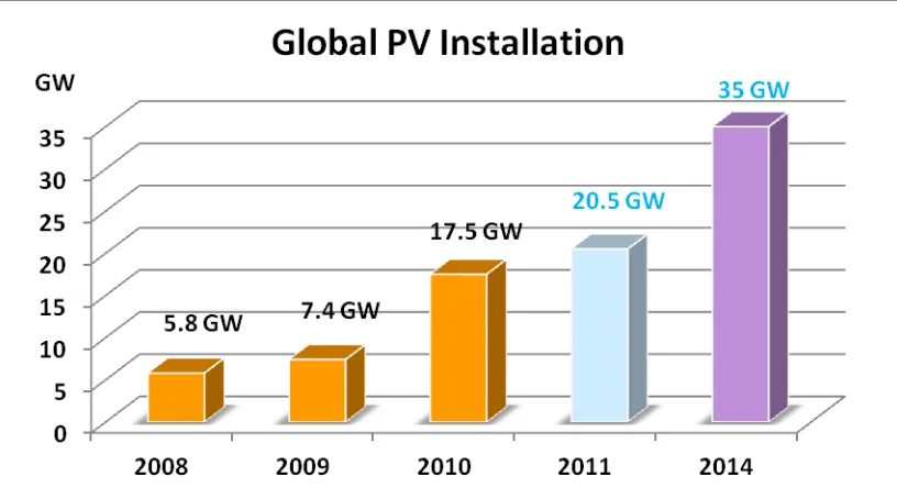
Fig. 1.1 Global PV Installation
Fig.1.2 shows the forecasts of installation growth in 2011 by system size. It is predicted that the very large scale utility PV plants will continue to dominate approximately 48% of the market share; small scale PV installations (<10kW) will account for about 33% of the total installation which implies that the residential scale of distributed PV energy generation will become increasingly important and popular with end users in the near future.
Meanwhile, large scale utilization of distributed renewable energy depends upon an advanced smart grid infrastructure where the users have the ability to manage their energy consumption as well as the use of plug-and-generate and plug-and-store energy devices at home and in industrial applications [6][7].
20 kVA SST
IEM
400V DC BUS120V AC
LOAD
DRER DESD
Communication
12kV AC Bus
LOAD DC DC UCAP/ Li-Ion DC DC PV DC AC Variable AC Generator
DGI
DRER IFM IFMThe FREEDM system is an intelligent electric power grid integrating highly distributed and scalable alternative generating sources and storage with existing power systems to facilitate a renewable energy based society [7]. The 400V DC bus in the FREEDM system provides an alternative interface for solar energy. Fig.1.3 shows part of the FREEDM system including an Intelligent Energy Management (IEM) module. As a result, PV converters in FREEDM system need only to have a DC/DC stage to perform Maximum Power Point Tracking (MPPT) and have a proper voltage conversion gain to interface with the DC bus.
The Solid State Transformer (SST) in IEM acts as an “energy hub” to do advanced power flow control as well as DC bus voltage regulation [7]. Generally, this structure has several advantages:
(1) Since the SST is the component interfacing with the electric grid, the PV converters’ controller does not require a phase locked loop (PLL), current regulator, or anti-islanding controller. Thus, the control task becomes much simpler.
(2) The PV converter can be comprised of a single power stage. Therefore, it is very likely to reduce the system cost for end users.
(a) PV String-level D-MPPT with a Centralized Inverter
(b) PV Module-level D-MPPT with a Centralized Inverter
Fig.1.4 Architecture of KW-MW Scale PV Application with Distributed MPPT [8] [9]
Moreover, from a system architecture point of view, this application has a similar structure as the advanced KW-MW scale PV application with central inverters (Fig.1.4) [8] [9]:
(2) In both applications, distributed MPPT (D-MPPT) technology is utilized to optimize the power output for each string (string-level D-MPPT) or even for each PV module (module-level D-MPPT). And the key element associated with the D-MPPT is the DC/DC converter.
Generally, the D-MPPT stage is usually comprised of a single DC/DC power stage with a MPPT controller. And the performance of the D-MPPT stage is critical to both systems. As a result, it becomes very important to research possible high performance solutions for the D-MPPT stage and this is also the key technology associated with the high efficiency power conversion in FREEDM systems.
1.2 Dissertation Outline
This research work focuses on development of high efficiency DC/DC converters as well as high performance power point tracking (MPPT) solution for distributed solar energy conversion in FREEDM systems and various scale PV applications.
The dissertation consists of six chapters. They are organized as follows:
Chapter I introduces background information and the motivation for this research.
reviewed and evaluated in terms of their efficiency, components count & size and other factors. These inverters are categorized from different points of view, such as the number of power processing stages and whether a transformer is used. Several important standards related to PV applications, i.e., IEEE 1547 [10] and the U.S. National Electrical Code (NEC) [11], are discussed and summarized. Also after the discussion of the requirements from the standards and the panel characteristics, a conclusion is drawn about whether PV panel side grounding is required. The objective of this part of work is to understand the requirements, challenges and new trends for solar energy conversion in the future.
VPV drops below a threshold voltage. Therefore, an efficiency-oriented design can be
executed and the converter can maintain high efficiency over an extended operation range. Both of the simulation and test results are provided to verify the feasibility of proposed converter. The results show that the experimental prototype’s weighted efficiency can reach 98%.
Chapter IV proposed PV module integrated converters (MICs) as a module-level D-MPPT stage which may result in a significant increase in the annual energy yield of this system. Mainly, there are two kinds of structures for PV-MICs: parallel connected structure and its counterpart, the series connected structure. A thorough comparison between these two structures is presented at the beginning of this Chapter. From the presented analysis, the parallel connected architecture was shown to have more advantages. But the challenge is also obvious: how to achieve high conversion gain with high efficiency. In this Chapter, a variable resonant tank (VRT) high efficiency resonant DC/DC converter is proposed for parallel connected DC MICs. This new topology may adapt resonant modes, depending on the panel operation conditions. By alternating the resonant tank structure, the converter may work at high efficiency in the low VPV condition and support a 400V DC bus with the help of an
operation principle of the proposed converter is explained in detail and a DC gain analysis is presented based on the fundamental harmonic analysis (FHA) method. The performance of the proposed VRT resonant converter was demonstrated on a 240W prototype when VPV
varies from 25V to 40V. The prototype’s maximum efficiency reaches 96.5% and an efficiency increase of more than 10% under light load conditions is shown when compared with a conventional LLC resonant converter.
perturbation step size and speed can be adjusted by the user. The operation principle of the new controller is explained and the cost evaluation is presented. The tracking performance of the proposed controller has been validated by both simulation and experimental results from a PV converter with 200W PV panels under different sun irradiation levels and temperatures.
Chapter 2. Grid-tied Solar Inverter
Technologies: An Overview
2.1 Basic Demands for PV Inverters
Since the grid-tied inverters are interfacing the PV modules with the grid, the standards given by the utility companies must be followed. At present, several particular standards and sections in U.S. National Electrical Code (NEC) [11] put more strict regulations for grid-connected solar inverters. For a solar inverter design, standards EN61000-3-2(applied in Europe) [14], IEEE1547 [10] and UL1741 [13] are worth considering. A summary of the requirements is listed in Table 2.1.
purpose is to avoid saturation of the distribution transformers [16].
Table 2.1 Summary of the Standards Related to Grid-tied PV Application [12]
including voltage disturbance and frequency disturbance. Table 2.2 and Table 2.3 below summarizes the required response time for inverters whose power ratings are less than 30kW.
Table 2.2 Inverter Response to Abnormal Grid Voltage [17] Voltage Range (% of base voltage) Clearing time (s)
V<50 0.16
50≤V<88 2
110<V<120 1
V>120 0.16
Table 2.3 Inverter Response to Abnormal Grid Frequency [17] Size Frequency Range (Hz) Clearing time (s)
≤30kW >60.5 0.16
<59.3 0.16
>30kW
>60.5 0.16 <{59.8-57.0} adjustable set-point adjustable 0.16 to 300
<57.0 0.16
disturbance (usually a current injection) into the grid and monitor the corresponding effect. This may affect the power quality and produce problems when large numbers of inverters are connected with the grid in parallel [18] [19]. IEEE Std.929-2000 [20] and IEEE Std. 1547 [10] both define several requirements for anti-islanding purposes. Several passive and active methods have been analyzed and tested in [18] and [19]. A drawback shared by all of these methods (except for the communication based ones) is that their successful detection rate is heavily load dependant and they may fail under certain load conditions. Only the communication based method is load independent. Considering that almost all of the solar inverters on the market have the communication capability, the cost to implement the communication based anti-islanding method into the inverter may be negligible. But a central monitoring system may be required to monitor the status of the grid and send out the commands to the solar inverters within range.
this may have significant impact on inverter design. These effects will be discussed later in this chapter.
For grid-connected inverters, there are two basic requirements for their functions: one is to ensure that the PV module(s) operates at the maximum power point; the other is to inject a sinusoidal current into the grid. In addition, inverters’ efficiency is quite an important index to evaluate an inverter’s performance. Usually efficiency is calculated according to the definition of European efficiency below:
EU 0.035%0.0610%0.1320%0.130%0.4850%0.2100% (2.1)
Another popular method to evaluate efficiency is based on the California Energy Commission (CEC) weighted efficiency formula:
CEC 0.0410%0.0520%0.1230%0.2150%0.5375%0.05100% (2.2)
Where the index value is equal to the percent of rated power [22]. For both calculation methods, the purpose for performing the six operating point efficiency calculation is to make a fair comparison of the inverters, under partial load conditions.
devices, soft switching techniques, and larger size heat-sinks to control the temperature rise, rather than using a fan.
2.2 Evolution of PV Converters: Past, Present and Future
The PV converter technology has a history of over half a century and is the key technology to power up satellites through PV panels in the aerospace application. In recent years, it has received considerably increasing attention worldwide due to the large demand for high efficiency solar energy application. There is a large amount of published literature related to PV converter technology.
The power rating of this centralized inverter is usually in the range of hundreds of KW or even MW. The centralized inverter usually has two kinds of DC bus voltage: 575V or 750V, depending on the grid side voltage. The advantage of this technology is the inverter’s high conversion efficiency and low cost per watt of produced electricity. However, this structure has several well known drawbacks, such as PV module mismatch losses, less flexibility to deal with partial shading and soiling conditions. In general, this architecture does not extract the maximum available energy that can be generated by the PV modules due to these drawbacks. The highest energy output is achievable only when all of the PV modules are exactly the same and the sun irradiation seen by each PV module is equal. Unfortunately, these conditions may never be met in practical solar applications due to variations of PV module parameters caused by temperature, aging and dust on the surface of modules. Also, partial shading caused by clouds, trees, and obstacles cannot be avoided completely. As a result, energy loss is relatively high in such a system, although the centralized inverter itself has a very attractive high efficiency.
will increase the complexity and cost of the system.
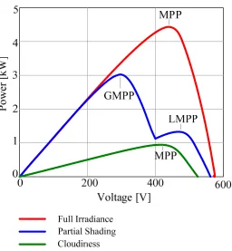
Fig. 2.2 Characteristic I-V and P-V Curves against Incident Radiation
Fig. 2.3 Characteristic P-V Curve of PV Panels under Different Conditions
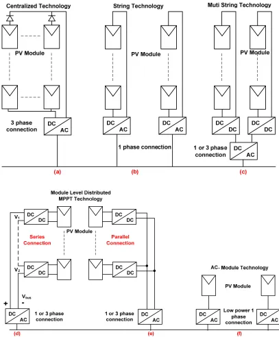
The present PV inverter technologies consist of the following: the string inverters (Fig. 2.1 (b)), the multi-string inverters (Fig. 2.1 (c)), the series/parallel connected power optimizer with centralized inverter (Fig. 2.1 (d) and Fig. 2.1 (e)), and the ac modules (Fig. 2.1 (f)).
inverter to interface with the electric grid. However, the negative effect of leakage current for the single stage solution should be evaluated in some cases. In practice, either advanced topology (i.e., H5 topology from SMA Inc) [29] or a low frequency transformer is used to solve the leakage current issue. More detailed discussion about leakage current’s impact on PV inverter design is presented in the next section.
The PV converter system structure shown in Fig. 2.1 (d), also known as the multi-string inverter, may increase year-round power generation in commercial or utility scale applications by taking advantage of string level distributed MPPT technology. A DC/DC converter is connected to a string of PV modules to fulfill the MPPT control for that string. The string level MPPT is achieved and it ensures that the negative effects of module shading, soiling, and aging mismatch, are minimized and contained within the string [30]. The DC/DC converter for each string may also boost the voltage to a higher level to allow the inverter to operate more efficiently. It is claimed that for this structure, the balance of system expense (BOS) may be reduced by 20-25% while gaining greater design flexibility [30]. Moreover, this solution is widely used in utility scale applications and it is receiving more attention from those solar inverter companies whose main products are high power centralized inverters.
The DC/DC converters in both types of structures may be called PV module integrated DC/DC converter (DC MIC). And particularly, the DC/DC converters in series connected structures are usually called solar power optimizers [31]. As shown in Fig. 2.1 (d), several DC MICs must form a series connection to obtain a voltage high enough for interfacing with the DC bus of the centralized inverter. The output current of the series connected DC MICs in a string remains the same. But their output voltage varies based on the amount of energy they can deliver. Assume only two DC MICs in series supporting DC bus in Fig. 2.1 (d), the following equations are valid:
VBUS V V1 2 (2.3) Ptotal VBUS I P P1 2 (V V1 2)I (2.4)
Where, I is the output current of MICs in this string; the Ptotal, P1 and P2 represent the total
generated power, output power of MIC 1 and output power of MIC 2, respectively. Apparently, the output voltage of MIC 1 and MIC 2 is proportional to its output power:
1 1 2 2
V P
V P (2.5)
V V1: ... :2 VN P P1: ... :2 PN
(2.6)
For the paralleled structure in Fig. 2.1 (e), multiple parallel connected MICs may interface with the DC bus directly. The basic requirement for MICs in this structure is that they need to have high conversion gain to support the DC bus considering the voltage for the single PV module is low. Fig. 2.4 and Fig. 2.5 present the pictures of both kinds of DC MICs products from Tigo Energy Inc.
Fig. 2.5 A Photograph of Distributed MPPT Stage for Structure in Fig. 2.1 (e) [32]
Generally, both series and parallel structures provide high flexibility in system design. The module level MPPT may greatly reduce the loss from partial shading and panel mismatch. Thus, optimized operation for each PV module may ensure the achievement of much better energy gain in practice. On the other hand, the two structures also differ in many ways and they have different features. A detailed analysis and comparison of their characteristics will be given in Chapter 4.
Fig. 2.6 A Picture to Demonstrate the AC Module Concept [33]
Table 2.4 Advantages of Micro-inverters and Module Level Distributed MPPT [23]
MICROINVERTERS DC-TO-DC
No specialized DC wiring or high-voltage components
Higher voltages=lower resistive losses in copper
Strong monitoring capabilities Strong monitoring capabilities No single point of failure Not necessary on every panel Enables DIY home owner and consumer sales
channels
High efficiency
Reduces cost of installation
inverters. Moreover, with continuous research effort and more companies entering this business field, the cost of micro-inverters is expected to decrease in the near future. Table 2.4 summarized the advantages of both micro-inverters and module level distributed MPPT technology.
The future technologies of PV inverters are a further extension of the development of present technologies, particularly, the PV converter structure (c), (d), (e), (f) in Fig. 2.1. The structure (c) may dominate the utility scale and commercial scale of PV applications in the future. The structure (d), (e) and (f) may receive large market shares in the residential and small commercial PV applications. Although it is hard to conclude which type of structure will prevail and dominate the market in the long run, it is pretty clear that the trend for PV converter technology is trying to squeeze out more energy from PV modules and reduce avoidable power loss. Although structure (c) has superior performance compared with conventional centralized structure, the system design and installation is still complex and expensive, requiring the installation site without any obvious obstacles and the PV modules in string should face the sun in a unified format. In such a system, maximum energy harvesting occurs only when every module in a string is matched exactly and the same amount of solar radiation reaches each solar cell in very module. From this point of view, this technology is realistically not a promising solution.
Considering that conversion efficiency is a primary concern for solar energy applications, it is s worthwhile to compare the efficiency of these promising solutions. Table 2.5 and Table 2.6 summarize the efficiency data based on datasheet of inverter products categorized in structures (c) ~ (f). Some companies in this area, like Tigo Energy Inc, Accurate Solar Inc and MPPC Inc, are not listed in the table because the efficiency data for their products are not published. In addition, the communication methods implemented in different micro-inverter products are also listed in Table 2.5.
Table 2.5 Efficiency Data of Micro-inverters
Micro Inverter
Company Prated (W) ηSYS
(CEC/EU)
Communication Type
Enphase 230/240 96% Powerline Carrier
Enecsys 200/240/280 94% Wireless IEEE. 15.4
Solar Bridge 235 94.2% Powerline Carrier
Petra Solar 200 93% Zigbee based Cellular Network
From Table 2.6, module level DMPPT solution has similar ηSYS as the string level DMPPT
with the DMPPT + Centralized Inverter solution. For the recently released Enphase products, their efficiency is about only 0.5% lower than the distributed MPPT solution.
Table 2.6 Efficiency Data of Distributed MPPT Stage + Centralized Inverter
String/Module Level Distributed MPPT (DMPPT)+ Centralized Inverter
Company
(DMPPT)
Company
(Inverter)
Structure Prated_DMPPT
(W) ηDMPPT (CEC/EU) ηINV (CEC/EU) ηSYS (highest)
Satcon SMA/ PV
Powered/ Satcon Inc
(>5kW)
Fig. 2.1 (c) 2.2K/2.9K 98.5% 97% ~ 98%
96.5%
Solar Edge Fig. 2.1 (d)
or Fig. 2.1 (e)
250/350 97.8% 95.8%
Azuray 250 98% 96%
Solar Magic 230 98.5% 96.5%
Fig. 2.8 Inverter Firm Market Share 2009 [23]
Table 2.7 Inverter Company Global Market Share (2006 ~ 2009) [23]
Inverter Manufacture 2006 MS% 2007 MS% 2008 MS% 2009 MS%
SMA 24% 33% 38% 40%
Ingeteam 3% 10% 6% 6%
Kaco 6% 7% 8% 8%
Fronius 10% 9% 8% 8%
2.3 Energy Yield Comparison of Different PV Inverter Technologies
The Energy yield is the key metric to compare the performance of different PV inverter technologies. Previous discussion pointed out that the distributed MPPT technologies may lead to lower conversion efficiency. However, placing the MPPT control at each module maximizes the power extraction and this begins to decrease as we move the MPPT closer to the central inverter. For systems with longer strings of series modules, partial shading has a more significant impact on the total generated power as compared to massively paralleled plants with high voltage PV modules, i.e., tandem amorphous silicon modules (VOC ~ 240V)
[24]. Also the annual energy yield increase by using distributed MPPT technologies is analyzed and quantified for several case studies in [24]. Table 2.8 ~ Table 2.9 gives the annual energy yield increase from partial shading for PV plants which consist of two types of PV modules: low voltage Si module or high voltage thin film module.
Table 2.8 Annual Energy Yield Increase from Partial Shading for Si Module Plant [24] MPPT
Location
Central DC/DC Converter
String Combiner
String Module System Location
Energy (kWh) 2,675,055 2,681,674 2,692,368 2,698,570 Phoenix, AZ 1,987,168 1,995,769 2,008,975 2,016,993 Newark, NJ % Yield Increase - 0.25% 0.65% 0.88% Phoenix, AZ
Table 2.9 Annual Energy Yield Increase from Partial Shading for High Voltage Thin Film Module Plant [24]
MPPT Location Central DC/DC Converter Array Combiner String Combiner
String Module System Location
Energy (kWh) 2328391 2336349 2338915 2338915 2341024 Phoenix, AZ 1704986 1715765 1719167 1719167 1722152 Newark, NJ % Yield
Increase
- 0.34% 0.45% 0.45% 0.54% Phoenix, AZ - 0.63% 0.83% 0.83% 1.01% Newark, NJ
Where the “array combiner”, “string combiner”, “string” and “module” mean to different MPPT locations. For example, if several PV arrays share a common MPPT, this arrangement is called “array combiner”. Similarly, if each PV string has its own MPPT, it is marked “string” in the table above.
The data in these table clearly show that by using distributed MPPT technologies, the annual energy yield increases in the range of 0.25% ~1.5% and for the plant with low voltage modules, the energy gain is even larger. This is because more low voltage modules are required to a form a string with a designed output voltage rating. And one key advantage of using distributed MPPT technologies is the increased availability of a power plant, since a failure in a single DC/DC converter does not lead to a complete plant shutdown [24].
Other factors affecting energy yield include:
level distributed MPPT.
Module mismatch, which may account for 0.5% ~ 1% gain in energy yield for distributed MPPT.
Converter efficiency. The drop in energy yield due to lower power conversion efficiency is estimated to range from 0.2% at the string combiner level to 1.9% for module level distributed MPPT.
MPPT algorithm, which may account for up to 2% of extra energy gain by moving it to a module converter.
2.4 Category of PV Inverter Topologies
PV inverter topologies can be categorized in terms of the number of power processing stages and whether a high frequency (HF) or low frequency (low frequency) transformer is utilized or not.
2.4.1. Number of Power Processing Stages
Fig. 2.9 depicted basic structure of single stage and multiple stage inverters.
Fig. 2.9 Three Types of PV Inverters: (a) Single Stage (b) Dual Stage (c) Dual Stage with Paralleled DC/DC Stage [12]
be calculated by:
2 sin (2 ) grid grid grid
p P t (2.7)
Where Pgrid is the average injected power, ωgrid is the angular frequency, and t represents
time. Since the pgrid varies at a frequency ωgrid and has a peak value of 2*Pgrid, the inverter
must be designed to handle a peak power level of twice the nominal power, according to equation (2.7). This structure is the typical configuration for a centralized inverter. At a certain maximum power point, since the power from the PV module is expected to be constant but the power delivered to the grid varies at a frequency of 2 ωgrid, power decoupling
capacitors must be added somewhere in the system. Fig. 2.10 shows possible power decoupling capacitors position in a system.
Fig. 2.10 Different Locations for the Power Decoupling Capacitor: (a) in Parallel with PV Modules (b) in Parallel with PV Modules or in DC Link [12]
Basically the size of the decoupling capacitor can be expressed as
ˆ 2
PV grid C C
P C
U u
Where Ppv is the nominal power of the PV modules, UC is the mean voltage across the
capacitor, and uˆCis the allowed amplitude of the ripple voltage. Equation (2.8) is based on
the fact that the current from the PV modules is pure dc and the current drawn from the grid-connected inverter follows a sin (2 )
gridt
waveform, assuming UC is constant.
Therefore, having a higher UC and larger allowable voltage variation at this decoupling
capacitor is beneficial to reduce the required capacitor size and extend the inverter’s lifetime. For a single stage inverter, CPV is the decoupling capacitor. In order to extract the maximum
possible energy from the PV modules, PV side voltage should be maintained at MPPT and does not allow for a large variation. Moreover, the single stage solution usually has a lower mean voltage on its decoupling capacitor CPV than the two stage solution where the DC link
capacitor CDC is chosen as the decoupling capacitor. These factors limit the capacitor size
reduction in the single stage inverter. For example, if Umpp=360V, uˆC is 2%*Umpp=7.2V,
Pmpp=2200W, a CPV of 1.15mF is required. On the contrary, if the capacitor is placed in the dc
link in two stage inverter (CDC in Fig. 2.10), it becomes 290μF at 500V with uˆC=20V
into sinusoidal waveform through SPWM modulation or space vector modulation [35] and the decoupling capacitor is usually placed at the DC link side. In the latter case, the dc-dc converter should be designed to handle a peak power of twice the nominal power; the required decoupling capacitor size is usually much larger since these capacitors are located at the PV module side (similar to the single stage inverter case). Obviously, there is no real DC bus at the DC link side for this case.
2.4.2. Transformers and Grounding
For commercial PV inverters, some of them utilize a transformer (either a high frequency transformer or a line frequency transformer). The transformer is a paradox inside the PV inverters. The answer to the question whether the transformer is required can have three aspects:
For the inverter itself: adding a transformer can be helpful to boost input voltage to a proper value when the input voltage is extremely low, such as in the AC module application; whereas the transformer is superfluous when the input voltage is sufficiently high.
most straightforward solution is to add a transformer.
It should be pointed out that the grounding requirement for Europe and the U.S is different. Floating PV systems are allowed in Europe and the filed application records show that such floating system is as safe as other grounding systems [21]. Usually a ground fault protection device (GFPD) is required for both the photovoltaic source and the output circuits. This device can detect a ground fault and automatically disconnects the conductors and /or shuts off the utility-interactive inverter or charge controller for that portion of the faulted array [11]. In the U.S. market, transformerless inverters are rare, particularly before 2005, since NEC690 (before 2005) requires all the PV systems should be grounded. It clearly pointed out that for residential applications, one of the conductors from the PV modules to the inverter circuit should be grounded. Since the neutral of either split phase transformer or 3-phase distribution transformer is grounded, one of the inverter’s output conductors connected with the grid is grounded when the inverter interfaces one phase in both cases. This kind of connection may bring trouble for the inverter design since a normal full-bridge inverter cannot be used as grid phase if there is not a transformer somewhere in the system. A few transformerless topologies can be grounded both at the input and at the output. These topologies will be discussed later.
several conditions. These changes further confirm that un-grounding PV system can be safe. Therefore from the standards point of view, grounding is no longer a requirement for the PV inverter design.
For the PV panel: basically, PV panels in the present market can be categorized into two types: Si crystalline type and thin film type. The crystalline type includes mono-crystal silicon and poly-crystal silicon. The mono-crystal technology is the oldest and its typical conversion efficiency is around 16%. Poly-crystal panels are widely used in today’s PV applications and its efficiency is approximately 15%. Compared with a crystalline panel, the thin film panel is less difficult to manufacture and exhibits relatively lower energy consumption. Thus the cost for manufacture of a thin film panel is lower than that of a crystalline one. Currently, thin film technology is more attractive and is expected to be used widely in the future after improvement of its conversion efficiency [36].
(Cp1, Cp2) whose value is in the range of 50-150nF/kW, depending on the weather conditions
and panel structure [37].
Fig. 2.11 Single Phase System with Parasitic Capacitances
In Fig. 2.11, the VPV+ and VPV- represents voltage potential applied to the positive and
negative conductors of the PV module. Although the differential voltage across the two conductors is constant DC in steady state, the VPV+ and VPV- themselves are not constant
voltage. Instead, VPV+ and VPV- may vary and contain high frequency components which are
highly dependent on the inverter circuit topologies and modulation methods. In other words, there is dv/dt between the module conductors and module frames since the frame is always firmly grounded. The leakage current can be calculated by the equations below:
1 1 ( PV ) lk P
d V
i C
dt
2 2 ( PV ) lk P
d V
i C
dt
(2.10)
Apparently, once a high enough dv/dt exists on the two conductors of PV module, a high leakage current will be induced which may flow between conductors and the ground. If the leakage current is sufficiently high, the GFPD may be triggered. Table 2.10 below gives the GFPD response time required by DIN VDE0126-1-1.
Table 2.10 Leakage Current Mean Levels and Response Time [38] Leakage Current Average
Value (mA)
Disconnect Time (s)
30 0.3
60 0.15
100 0.04
To limit the leakage current as well as to avoid the potential problems arises from high leakage current, the following solution may be considered:
Grounding one of the conductors of PV module. For most PV modules, the negative conductor may be grounded. The grounding may bring two advantages. First, the parasitic capacitance Cp2 is eliminated. Second, the dv/dt on the positive conductor can be greatly
reduced because it is only related to the voltage ripples on the PV side filter capacitor CPV. In
an ideal case (i.e., CPV size is infinite large), the dv/dt should go to zero. In practice, its value
Eliminate or reduce the dv/dt applied to the parasitic capacitors. This may be achieved by elimination/reduction of the high frequency components in VPV+and VPV-.
Generally, both solutions mentioned above are based on modification of the inverter circuit. To achieve the PV module side grounding, adding a transformer is a common solution otherwise advanced transformerless inverter topologies with grounding capability need to be developed. Similarly, in order to eliminate/reduce the dv/dt, advanced new inverter topologies are required.
Table 2.11 Leakage Current Comparison Results [37] Topology FB Bipolar FB
Unipolar
NPC 3FB 3xNPC 3xHB
Nr. Of Input Capacitors
1 1 2 1 2 2
Nr. Of Switches 4 4 4 6 12 6
Bypass Diodes - - 2 - 6 -
DC to Ground voltage (peak value
and frequency)
Vgrid/2,
50Hz
±Vdc,
10kHz
1% Vdc ±Vdc,
10kHz
1% Vdc 1% dc
Leakage Current (peak values)
< 30mA >> 5A <30mA >> 5A <30mA <30mA
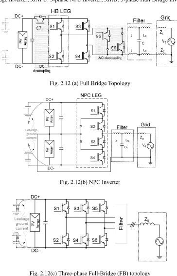
Several transformers-less inverter topologies have been investigated in [37] to evaluate their leakage current and the voltage imposed at the PV module conductors. Fig. 2.12 below shows topologies evaluated in [37] and Table 2.11 summarized the evaluation results.
Full Bridge Inverter; 3xNPC: 3-phase NPC Inverter; 3xHB: 3-phase Half Bridge Inverter.
Fig. 2.12 (a) Full Bridge Topology
Fig. 2.12(b) NPC Inverter
Fig. 2.12(d) 3xNPC Used for a Three Phase System
Fig. 2.12(e) Half-bridge Legs Used to Supply a Three Phase System Fig. 2.12 Several Transformerless Inverter Topologies Used for Evaluation [37]
single phase full-bridge topology can only use bipolar PWM strategy because using unipolar switching will produce ±Vdc voltage jump at the switching frequency on the PV module
conductors, generating high leakage currents. Same results have been seen on the 3-phase FB. Better results are achieved with NPC, 3xNPC and 3xHB because of the grounding of the middle point of the input capacitors. In this case, the voltage fluctuation is reduced to only several volts [37].
Further studies have shown that more attention should be put onto those applications with thin film PV modules since these types of PV modules are much more sensitive to the leakage current [39]. This is because of the lack of additional isolation from the outside environment afforded by the “ethylene vinyl acetate” (EVA) encapsulate between the Si solar cells and the top glass sheet [40]. Researchers in NREL applied voltage, water vapor and light stresses to thin-film PV modules with SnO2F transparent conducting oxides (TCOs)
deposited on the soda-lime glass super-stratum and evaluated the corrosion of the thin-film layers under different conditions.
showed no visible corrosion. Also Fig. 2.13 (b) shows the damage area percentage increases more rapidly with higher ambient temperature. The formation of this corrosion is due to the transport of positive charged sodium ions from a module front glass into the TCO layer in thin film panels.
(a) bar-graphing (b) corrosion comparison Fig. 2.13 Accelerated Test Results in NREL Report [40].
In summary, two conclusions can be drawn from the above discussion:
The floating PV system is allowed and no grounding requirement is from the electrical standards & codes point of view.
grounding of the negative conductor cannot be achieved, eliminating/reducing the dv/dt on the conductors may also benefit PV modules, including crystalline and thin-film modules.
For some other special PV modules, such as highly efficient back-side contact cells developed by Sun-Power in 2005, there may be special requirements. This kind of module needs the positive conductor grounded, in order to eliminate negative charges in the panel front surface [41].
2.4.3. Trends and Present Development
Since thin-film modules (or other newly developed PV modules) may become more important in the future PV module market, a PV inverter should have the capability to make one pole from the panel side to be grounded; or the dv/dt on the conductor poles of PV module can be controlled to be in an acceptable range. Considering these facts, the development of future PV inverter may follow two different trends:
transformerless inverters: it is easier to realize high efficiency. Thus the objective for transformerless inverters is to reduce the PV module side voltage fluctuation (dv/dt) or, if possible, achieve PV side positive/negative pole grounding.
which can be compared with that of transformerless inverters.
In recent years, several transformerless PV inverter topologies have been proposed to achieve panel side grounding. Fig. 2.14 below shows a grid connected half-bridge 3-level NPC inverter (HBDC) [28] [42], which is the same as the one in Fig. 2.13 (b). As stated previously, the middle-point of the capacitor can be grounded and thus the voltage fluctuation and parasitic capacitance can be reduced. In HBDC, one of the PV modules’ positive conductors is grounded and both the DC side and the AC side can be grounded. This connection is safe for crystalline modules but is not allowed for thin-film PV modules and thus the use of this topology is limited. Another drawback of this topology is the two PV strings are loaded alternatively with line frequency rather than continuously. Thus the decoupling capacitor size should be enlarged.
Fig. 2.14 HBDC Inverter Topology [28] [42]
circuit (GCC) which can load each PV string independently [43] [44]. The advantage of GCC is that individual MPPT can be applied to each string. Actually, one of the PV strings can be removed and sinusoidal current can still be injected into the grid. In this case, this structure can be used with various types of PV panels and realize grounding for both DC side and AC side.
Fig. 2.15 PV Inverter with GCC [43] [44]
module side. Fig. 2.18 gives the simulation results.
Fig. 2.16 HERIC Topology [32]
time/mSecs 10mSecs/div
0 10 20 30 40 50
V -300 -200 -100 0 100 200 300
HERIC topology DC side voltage (red: positive pole blue: negative pole)
(a) HERIC Simulation Results
time/mSecs 10mSecs/div
0 10 20 30 40 50
V -500 -400 -300 -200 -100 0 100 200 300 400
H5 topology DC side voltage fluctuation(green: positive pole red: negative pole)
(b) H5 Topology Simulation Results
Fig. 2.18 Simulation Results to Verify PV Module Side Voltage Fluctuation of HERIC and H5 Topologies
2
sin( )
2
PV m
V
V
wt
V
(2.11)2
sin( )
2
PV m
V
V
wt
V
(2.12)In the case of H5 topology, it has the same component of line frequency voltage with a small amount of high frequency ripple. Therefore, both of these two topologies may reduce the leakage current. However, since the negative conductor has a negative voltage potential relative to the ground, these topologies cannot be used with thin-film panels. The commercialized product from Sunways has 2-5kW inverters with euro-efficiency around 95%. Product SB8000TL (8kW power rating) from SMA using H5 topology has a CEC weighted efficiency of approximately 98%.
up to 97% [49].
Fig. 2.19 Karschny Topology [49]
Fig. 2.21 One Phase Connection of Inverter in [50]
Based on the analysis above, the converters in Fig. 2.14 and Fig. 2.15 can be used with the panels which require one of the conductors grounded. Moreover, converters in Fig. 2.19 and Fig. 2.20 may only support negative conductor grounding.
utilizing the step up/down feature of the transformer. Besides the line frequency transformer, high frequency transformers are also widely used in high power PV inverters.
In the case of string/multi string inverters for residential application (power rating below 10kW), most are connected to one phase and the neutral is at the grid side. In the U.S., they are typically connected with two phases of a split-phase distribution transformer with a typical RMS voltage equal to 240V, as shown in Fig. 2.22. In this case, several modifications should be added to the transformers-less inverters shown in Fig. 2.19 ~ Fig. 2.20. Otherwise they will not work properly if the PV side negative conductor is grounded.
Fig. 2.22 Two Possible Connections between Inverter and Grid
(a) Topology for Multi-String Inverter in [12]: Sunny Boy 5000TL
Most of the inverters for AC module application are based on a typical Flyback converter or its enhanced versions. Fig. 17 depicts several topologies proposed for AC module [12]. The reasons for using this type of topology are as follow:
Flyback converter inherently can boost the input voltage and meet the voltage requirement for grid connecting since the module side voltage is only 25V~ 55V.
Considering the topology limitations [62], the power rating of Flyback converter is usually in the range of several hundred watts, which is a good match of that of AC module.
Only one transistor is required on the primary side and no inductor is required at the Flyback output. Thus, it results in a lower cost design.
Like the Flyback application in power factor correction (PFC), it may regulate the output current in a way that the envelop line of output current becomes a rectified sine wave. After unfolding circuitry and filters, a sinusoidal current is reproduced which may be fed into the grid.
The disadvantages of this type of inverter are as follow:
The voltage stress of the switch in primary side is equal to the sum of the input voltage and the output voltage divided by transformer’s turn ratio, which is usually 2-3 times of input voltage.
Thus, several voltage clamp circuits or enhanced version Flyback converters are proposed to clamp the voltage. The active clamp transformer reset technique offers many well-documented advantages over traditional single-ended reset techniques, including lower voltage stress on the main MOSFET, the ability to switch at zero voltage, reduced EMI and duty cycle operation above 50%. The active clamp circuit may be applied to either the low side of the transformer (Fig. 2.24) or the high side of the transformer (Fig. 2.25). The differences between the two types of circuit are analyzed in [52] and Table 2.12 gives a summary of the comparison results.
Fig. 2.25 High-Side Active Clamped Flyback Converter [52]
Table 2.12 Comparison between High-Side Active Clamp and Low-side Active Clamp [52]
full sine wave. The first three utilize an additional secondary winding of the transformer together with several more switches to rebuild the sinusoidal current. For the last two in Fig. 2.26 (d) and Fig. 2.26 (g), the AC module utilizes a thyristor or MOSFET bridge to unfold the current. The added switches or the thyristors are switched at the line frequency and as a result, there is no apparent additional switching loss. Another topology proposed for AC module is the one shown in Fig. 2.26 (f): a series-resonant dc-dc converter with bang-bang dc-ac inverter [1]. The advantages of this topology are soft-switching for SPV1 and SPV2 and
the compact design of the transformer due to it ability to operate at a much higher switching frequency.
Fig. 2.26(b) Modified Shimizu Inverter [54]
Fig. 2.26(c) Dual Transistors Flyback-Type Inverter [55]
Fig. 2.26(e) Flyback dc/dc Converter with a PWM Inverter [57] [58]
Fig. 2.26(f) Series-Resonant dc-dc Converter with Bang-Bang controlled dc-ac Inverter [59]
Fig. 2.26(g) Soladin 120 Commercialized Inverter [60] Fig. 2.26 Several Inverter Topologies for AC Module Application
Table 2.13 Summery of AC Module Inverters [12] Fig. No. Decoupling capacitor lifetime Grid interface European Efficiency Cost [Euro] Component ratings (besides EMI filter)
- - - - - - T[cm^3] S+D [KVA]
Fig.
2.23(a)
2.2mF@45V Medium
2 transistor
CSI
91.4% 19.6 0.0115 12.3
Fig.
2.23(b)
68uF@160V Short
2 transistor
CSI
69.7% 27.6 0.0173 36.5
Fig.
2.23(c)
2.2mF@45V Medium
2 transistor
CSI
92% 22.6 0.0115 13.7
Fig.
2.23(d)
2.2mF@45V Medium
4 transistor
CSI
92.4% 20.7 0.0115 16
Fig.
2.23(e)
33uF@400V Long
4 transistor
VSI
90.3% 19.4 0.0081 14
Fig.
2.23(f)
33uF@400V Long
4 transistor
VSI
90.5% 25.3 0.0041 13.3
Fig.
2.23(g)
2.2mF@45V Medium
4 transistor
CSI
95.4% 21.1 0.0115 18.5
since the magnetic component size is minimized. The Flyback based converter attains a good balance between the efficiency and cost, and the topology in Fig. 2.26 (d) has a very practical value. The converter in Fig. 2.26 (b) has lowest efficiency and largest device rating. Also, the typical efficiency of these AC modules is around 90%-95.4% (except converter in Fig. 2.26 (b)).
2.5 Summary
This chapter discussed the roadmap for development of grid-tied solar inverters. The evolution of the solar inverter technologies has two aspects: system structures and inverter topologies. Therefore, the content of this chapter may be divided into two parts.
the advantages as well as disadvantages of different structures. The energy yield for different PV inverter structures is compared and energy gain is listed in the second section. The comparison showed that a year round energy yield gain in the range of 4% ~ 12% may be obtained for the system using distributed MPPT technologies over centralized inverter systems.
In the second part of this chapter (Section 2.4), various PV inverter topologies are reviewed and evaluated in terms of their efficiency, component count & size and other factors. These inverters are categorized according to different aspects, such as the number of power processing stages and whether a transformer is used. Several important standards related to PV applications are discussed and summarized. Also after the discussion of the requirements from the standards and the panel characteristics, a conclusion is drawn about whether PV panel side grounding is required.
The objective of this part of the project is to understand the requirements, challenges and new trends for solar energy conversion in the future. Generally, future research related to high efficiency PV energy conversion will focus on the following aspects:
The investigation and development of new PV system structures.
Chapter 3. “Hybrid Bridge” High Efficiency
Resonant DC/DC Converter for String Level
Distributed MPPT Applications
3.1 Research Motivation
The discussion in Chapter 2 pointed out that although PV module side grounding is not required by the corresponding standards both in Europe and the U.S., a versatile PV inverter should have the capability of PV module side grounding or at least, have the capability to control the dv/dt on the PV module conductors to avoid excessive leakage current.
As shown in Fig.3.1, for commercial and utility scale PV applications, string level distributed MPPT technology (also referred as multi-string inverter), may increase the year-round energy yield by utilizing individual MPPT controller for each PV string. The string level MPPT ensures that the negative effects of module shading, soiling, aging and mismatch are minimized and contained within the string.
Fig.3.1 String Level Distributed MPPT Technology Depicted in Fig. 2.1 (c)
Schottky Diodes. However, this solution may require an additional line frequency transformer at the output of the inverter stage if it is the objective of the PV system to achieve the PV module side grounding [63]. Apparently, the line frequency transformer will arrive at a solution which is both more expensive and heavier.
Fig.3.3 DC Gain Characteristics of the Half Bridge LLC Resonant DC/DC Converter [67]
During each switching cycle, the resonant component Lm joins the resonance between Lr
and Cr only for a part time. Thus, the LLC resonant converter has two resonant frequencies
shown as below [67]:
1 2
s
r r f
L C
(3.1) 1
2 ( )
m
m r r
f
L L C
(3.2)
![Table 2.1 Summary of the Standards Related to Grid-tied PV Application [12]](https://thumb-us.123doks.com/thumbv2/123dok_us/1489856.1182293/30.612.94.503.170.600/table-summary-standards-related-grid-tied-pv-application.webp)

![Table 2.4 Advantages of Micro-inverters and Module Level Distributed MPPT [23]](https://thumb-us.123doks.com/thumbv2/123dok_us/1489856.1182293/44.612.163.468.73.286/table-advantages-micro-inverters-module-level-distributed-mppt.webp)
![Table 2.7 Inverter Company Global Market Share (2006 ~ 2009) [23]](https://thumb-us.123doks.com/thumbv2/123dok_us/1489856.1182293/49.612.185.447.107.370/table-inverter-company-global-market-share.webp)
![Fig. 2.13 Accelerated Test Results in NREL Report [40].](https://thumb-us.123doks.com/thumbv2/123dok_us/1489856.1182293/65.612.300.491.235.387/fig-accelerated-test-results-nrel-report.webp)
![Fig. 2.17 H5-Topology [32]](https://thumb-us.123doks.com/thumbv2/123dok_us/1489856.1182293/69.612.145.492.136.604/fig-h-topology.webp)
