Grid-Connected Photovoltaic System Based
On the Switched Coupled - Inductor
Quasi-Z- Source Inverter
K.P.Nithya1, Soumi Pattanayak2, B.Rishana3, R.Aishvarya4
Assistant Professor, EEE, Panimalar Institute of Technology, Chennai, Tamil Nadu, India1 Fourth Year BE, Dept. of EEE, Panimalar Institute of Technology, Chennai, Tamil Nadu, India2 Fourth Year BE, Dept. of EEE, Panimalar Institute of Technology, Chennai, Tamil Nadu, India3 Fourth Year BE, Dept. of EEE, Panimalar Institute of Technology, Chennai, Tamil Nadu, India4
ABSTRACT: Embedded switched-inductor Z-source inverters have become a research hotspot because of their single-stage buck-boost inversion ability. However, their boost gains are limited because of complex component-voltage stresses and poor output power quality .To overcome these drawbacks, a new high-voltage boost impedance-source inverter called a switched-coupled-inductor quasi-Z-source inverter is proposed .The proposed inverters provide a high boost voltage inversion ability, a lower voltage stress across the active switching devices, a continuous input current and a reduced voltage stress on the capacitors. In addition, they can reduce the start up inrush current, which otherwise might destroy the devices. The proposed inverter adds only one capacitor and two diodes to a classical quasi-Z-source inverter, and even with a turns ratio of 1:1, it has stronger voltage boost-inversion ability than existing high-voltage boost quasi-Z-source inverter topologies. This paper grants the operating principles, analysis, and simulation results, and compares them to the conventional embedded switched-inductor Z-source inverter. To validate its advantages, analytical, simulation, and experimental results are also presented.
KEYWORDS: SCL-qZSI, qZSI, inrush current and PV-system
I.INTRODUCTION
Conventional voltage and current source inverters (VSIs and CSIs, respectively) [1], [2], in spite of their huge demand in industrial applications they suffer from some serious drawbacks, which make them less attractive. In specific, VSIs can perform only buck operations, while CSIs can perform only voltage boost inversions. Therefore, in applications that requireboth buck and boost operations, an additional dc-dc converter is needed, resulting in a two-stage power conversion with a higher system cost and volume, low efficiency, and complex control [3].
Z-source inverters were proposed [4] in order to achieve buck-boost abilities. In the Z-source inverter, both the switches in a leg can be turned on at the same time and therefore the dead time is eliminated. This significantly improves the reliability and reduces the waveform distortion. Various Z-source inverter topologies have been stated in many different studies.
Some papers have recently focused on the improvement of the boost factor of the Z-source inverter by using a very high modulation index in order to achieve better output waveform. For studies [7]-[8] add inductors, capacitors, and diodes to the Z-impendence network in order to produce a high dc voltage from a very low input dc voltage. These topologies outfit solar cell and fuel cell applications, since they require a high voltage gain in order to match the source voltage to the line voltage.
boosting ability. This paper can reduce the startup inrush current, lower the component-voltage stresses, and provide better output power quality ,which where the drawbacks of embedded switched-inductor Z-source inverter.
II.TRADITIONAL EMBEDDED SWITCHED-INDUCTOR Z-SOURCE INVERTER:
Fig.1 Embedded switched-inductor Z-source inverters
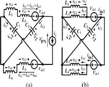
Fig. 1 shows the embedded switched-inductor Z-source inverters, having two separate dc sources .The difference between the proposed topologies and the ESL-ZSI topology is the positions of the dc sources and the number of components used. Fig.2 represents the operating states of ESL-ZSI.
Fig. 2.(a) Non-shoot-through Operating states and (b) Shoot-through Operating states of Embedded switched-inductor Z-source inverters.
The ESL-ZSI has two operating state , they are shoot-through and non-shoot through states.The inverter main circuit has six active states and two zero states. During the non-shoot-through state, Din, D5 and D6will beforward biased,
whereas D1, D2, D3 and D4will bereverse biased. So L1 and L3will be connected in series; L2 and L4will also be
connected in series. As a result Capacitors C1 and C2will be charged.Then the inductors L1, L2, L3, and L4 will transfer
energy to the main circuit. The corresponding voltages across L1, L2, L3 and L4 in this state are VL1_nonshoot , VL2_non shoot ,
VL3_non shoot and VL4_non shoot, respectively. In the shoot-through states,the inverter is short circuited by upper and lower
switching devices in the phase legs. During the shoot-through state, Din, D5 and D6will be reverse biased, whereas D1,
D2, D3 and D4will be forward biased. So L1 and L3will be connected in parallel; L2 and L4will also be connected in
energy.Since each dc source is directly connected to the switched-inductor cell (L1-L3-D1-D3-D5 or L2-L4-D2-D4-D6).
Therefore, a ripple appears on the input current of this topology. So the boost factor of theESL-ZSI, B is defined by:
. 3 1
1 D D B
III.PROPOSEDSCL-QZSI
Fig. 3 shows the circuit of the proposed SCL-qZSI .The proposed inverter consists of three diodes (Din , D1 ,
and D2 ), three capacitors (C1, C2, and C3 ), an input inductor L1 , and an SCLwith three windings (N1 , N2,
andN3 ). Windings N1 and N2 have the same number of turns (N1- N2 ), and the turn ratio of windings N3to
N1 (or N2 ) is n,(n=N3/N1=N3/N2).
Fig. 3. Proposed switched-coupled-inductor quasi-Z-source inverter The advantages of the proposed SCL-qZSI are as follows:
1. It reduces the starting inrush current.
2. Since the SCL is in series with switched-capacitor C3,the inrush of C3is reduced.
3. The energy stored in the leakage inductance is absorbed by capacitorC2.Hencethere is no voltage spikes due to
switching.
4. It has a boost factor of3/(1-4D) , which is higher than that of the ESL-ZSI. 5. It provides lower component-voltage stresses and better output power quality. 6. Core size of the input inductor L1 in the proposed SCL-qZSI is small.
A.OPERATING PRINCIPLEOF THE SCL-QZSI:
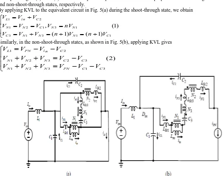
The proposed inverter has shoot-through zero states in addition to the traditional six active states and two zero states. For analytical purposes, the operating states may be simplified as shoot-through and non-shoot-through states. The equivalent circuits of the proposed inverter during these states are given in Figs. 4(a) and (b), in which a detailed SCL model is shown, including the magnetizing inductance. Llk1, Llk2, and Llk3are the leakage inductance of windings N1, N2,
and N3 respectively.
A.Shoot-through state:Fig. 4(a) represents the equivalent circuit of the proposed inverter during the shoot-through state, which is obtained by simultaneously closing both the switches of phase leg. During this state, diode Din is reverse
biased while diodes D1and D2 are forward biased. Windings N1 and N2 are energized with C1 in parallel. C3 gets
energizedby C1 through winding N3 , which increases the boost factor. leakage inductance of the SCL is used to limit
the charging current of C3.
B.shoot-through state:This state consists of six active states and two zerostates .The equivalent circuit of the Non-shoot-through state is shown in Fig. 4(b). During this state, diode Din is forward biased while D1and D2arereverse
biased. So Capacitors C1and C2 will be charged.Since the windings (N1 , N2 , and N3 ) and capacitor C3 are in series
B.BOOST ABILITY OF SCL:
The boost factor B of the SCL-qZSI network is the ratio of the dc-link voltage of the inverter-bridge VPN to the input
dc-voltage Vin. Due totrifilar windings the leakage inductance of the SCL is very small.Similar to the derivation of the
boost factor for trans-ZSIs [11]-[15]; the leakage inductance is eliminated in order to derive the boost factor of the SCL-qZSI. Figs. 5(a) and 6(b)show the simplified equivalent circuits ofthe proposed inverter during the shoot-through and non-shoot-through states, respectively.
By applying KVL to the equivalent circuit in Fig. 5(a) during the shoot-through state, we obtain
) 1 ( ) 1 ( ) 1 ( , 1 1 3 1 3 1 3 1 2 1 2 1 C N N N C N N C N N C n i L V n V n V V V nV V V V V V V V
Similarly, in the non-shoot-through states, as shown in Fig. 5(b), applying KVL gives
)
2
(
3 1 3 2 1 3 2 3 2 1 2 1
C C PN N N N C C N N N C n i PN LV
V
V
V
V
V
V
V
V
V
V
V
V
V
V
Fig: 4 Equivalent circuit of the proposed SCL-qZSI during (a) the shoot-through state, and (b) the non-shoot-through state.
Due to magnetic coupling VN3= nVN2=nVN1, evenduring non- shoot –through state ,VC3 = (n+1) VC1.Therefore,(2) can
be modified as follows: VN1 =
𝑉𝐶2−𝑉 𝐶3
2+𝑛 (3)
VN1 =
𝑉𝑃𝑁
𝑛+2 -
𝑉𝐶3
𝑛+1 (4)
If D is the shoot-through duty, then DT is the shoot-through time interval and (1-D)T is the non- shoot-through time interval .Applying the voltage-second balance condition on inductor L1 from (1) and(2) gives
VPN =
1
1−𝐷 (Vin +VC2) (5)
Similarly, applying the voltage-second balance condition on winding N1 from (1) and (3), we obtain
Again, applying the voltage-second balance condition on winding N1 or N2 from (1) and (4), gives
)
7
(
2
)
1
)(
1
(
3 PN CV
n
D
n
V
Again, applying the voltage-second balance condition on Substituting (6) in (7) ,yields
) 8 ( 2 1 2 PN C V n D n V
From (5) and (8),the dc-link voltage across the inverter-bridge can be expressed as,
) 9 ( ) ) 3 ( 1 ( 1 in PN V D n n V
Therefore, the boost factor of the proposed SCL-qZSI is given by ) 10 ( ) 3 ( 1 ( 2 D n n V V B in PN
When the turn ratio n is 1, the boost factor becomes
) 11 ( ) 4 1 ( 3 D V V B in PN
For the sake of comparison, Fig. 6 shows a plot of the boost B factor D versus for the proposed SCL-qZSI, ESL-ZSI, SL-qZSI, and qZSI. From this figure, it can be seen that the boost ability of the proposed inverter is significantly higher than the other topologies.
For the simple boost control method, the relation between the modulation index M and shoot-through duty ratio D can be expressed as,
) 12 ( 1
0 M
T T
D
Where T0 and T are the shoot –through time interval and time period, respectively.
By substituting (12) into (11), the boost factor B oftheproposed SCL-qZSI can be expressed in terms of themodulation index M as,
) 13 ( 3 4
3
M B
The output peak phase voltage
ph
V
of the inverter is given by, )
14 ( 2 2
in PN
ph
MBV MV
V
From (13) and (14), the voltage gain G( MB) of the proposed inverter can be written as,
) 15 ( 3 4
3 ) 2 /
(
M M V
Vph G
in
Fig .7 shows a plot of the voltage gain G versus themodulation index M for the proposed SCL-qZSI, ESL-ZSI,SL-qZSI, and qZSI. From Fig. 7, it can be observed that the voltage gain G increases with a decrease in the modulation index, and for the same modulation index M , the proposed inverter has a higher voltage conversion ratio than the other topologies. Therefore, for the same voltage conversion ratio, the proposed SCL-qZSI makes use of the larger modulation index.
IV.RESULTSANDDISCUSSION
In order to verify the above mentioned theoretical analysis, simulations are performed for the proposed SCL-qZSI to produce output ac-voltage of 220 Vrms (line-to-line) from the input dc-voltage of 50 V. The simulation parameters
selected are L1=320μH, C1=C2=C3=50μH, and the magnetizing and leakage inductances of the SCL are 100μH and
0.1μH respectively. The simulation used a resistive load of and a switching frequency of 20 kHz. 50/ phase.The simulation parameters are also listed in Table I. When simple boost control method is used, a voltage conversion ratio G of 4.5 is needed. The values of the various parametersare,D=0.1,B=5,VPN=415V,VC1=125V,VC2=290V, and VC3=
250V
TABLE-I ELECTRICAL SPECIFICATION OF THE PROPOSED INVERTER
Input voltage 50Vdc
Output voltage 220Vrms(line-line) Z-source capacitor(C1,C2,C3) 50Μf
Z-source inductor ,Lⁿ 320μH
Coupled inductor (n=1)
LN1,LN2,
LN3
Lm=100 μH ,
L1k=.1μH
Output filter inductor(Lf) 330 μH
Output filter capacitor(Cf) 50 μF
Fig 8: For the proposed SCL-qZSI(a) Three-phase output line-to-line ac-voltage and (b) input dc-voltage
(a) (b)
Fig:9 For the proposed SCL-qZSI (a) Capacitor voltages (b) and dc-link voltage
Fig.8(a), (b), and Fig. 9(a), (b) show the simulation results of the proposed inverter for M=0.9 , which are identically matching to the theoretical analysis. The voltages across capacitors C1, C2, andC3 are boosted to 125 V, 290 V, and
250V, respectively, whereas the dc-link voltage is boosted to 415 V.
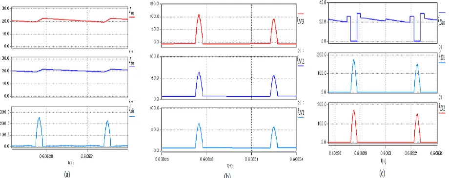
Fig. 10. Simulation results of the proposed SCL-qZSI for M = 0.9. (a) Input inductor current, magnetizing current, and shoot-through current. (b) Winding currents. (c) Diode currents.
V.CONCLUSION
power quality, which are attributed to the use of a lower modulation index. The proposed topology is obtained by combining the switched-capacitor SC and a three-winding SCL into the classical qZSI. The charging of the SC through the SCL significantly enhances the boostability of the proposed inverter, without increasing the turn ratio of the SCL.The proposed inverter reduces the starting inrush current.
The proposed inverter is best suited for applications that require a single-stage high step-up boost inversion of low dc-voltage sources such as fuel cells and PV systems. A comprehensive theoretical analysis of the proposed inverter was performed, and we successfully verified its performance through simulations results.
REFERENCES
[1]R. R. Errabelli, and P. Mutschler, “Fault- tolerant voltage source inverter for permanent magnet drives,” IEEE Trans. Power Electron., vol. 27, no. 2, pp. 500-508, Feb. 2012.
[2] B. Sahan, S. V. Araujo, C. Noding, and P. Zacharias, “Comparative evaluation of three-phase current source inverters for grid interfacing of distributed and renewable energy systems,” IEEE Trans. Power Electron., vol. 26, no. 8, pp. 2304-2318, Aug. 2011
[3] M. Shen, A. Joseph, J. Wang, F. Z. Peng, and D. J. Adams, “Comparison of traditional inverters and Z-source inverter for fuel cell vehicles,” IEEE Trans. Power Electron., vol. 22, no. 4, pp. 1453–1463, Jul. 2007.
[4] F. Z. Peng, “Z-source inverter,” IEEE Trans. Ind. Appl., Vol. 39, No. 2, pp. 504-510, March/April 2003. [5]J. Anderson, and F. Z. Peng, “Four quasi-Z-source inverters,” in Proc. IEEE PESC’08, 2008, pp. 2743-2749.
[6]J. H. Park, H. G. Kim, E. C. Nho, and T. W. Chun, “Power conditioning system for a grid connected PV power generation using a quasi-Z-source inverter,” Journal of Power Electronics, Vol. 10, No. 1, pp. 79-84, 2010.
[7]M. Zhu, K. Yu, and F. L. Luo, “Switched-inductor Z-source inverter,” IEEE Trans. Power Electron., Vol. 25, No. 8, pp. 2150-2158, Aug. 2010. [8]M. K. Nguyen, Y. C. Lim, and G. B. Cho, “Switched-inductor quasi-Z-source inverter,” IEEE Trans. Power Electron., Vol. 26, No. 11, pp. 3183-3191, Nov. 2011.
[9]C. J. Gajanayake, F. L. Luo, H. B. Gooi, P. L. So, and L. K. Siow, “Extended boost Z-source inverters,” IEEE Trans. Power Electron., Vol. 25, No. 10, pp. 2642 - 2652, Oct. 2010.
[10] S.-M. Chen, T.-J.Liang, K.-H.Chen, M.-L.Lao, and Y.-C. Shen, “A novel switched-coupled-inductor dc-dc step-up converter,” in Energy Conversion Congress and Exposition (ECCE), 2013, pp. 1830-1833.
[11] W. Qian, F. Z. Peng, and H. Cha, “Trans-Z-source inverters,” IEEE Trans. Power Electron., vol. 26, no. 12, pp. 3453–3463, Dec. 2011. [12] M. Adamowicz, R. Strzelecki, F. Z. Peng, J. Guzinski, and H. A. Rub, “New type LCCTZ-Z-source inverters,” in Proc. Eur. Conf. Power Electron. Appl., 2011, pp. 1-10.
[13] M.-K. Nguyen, Y.-C.Lim, and S.-J. Park “Improved trans-Z-source inverter with continuous input current and boost inversion capability,” IEEE Trans. Power Electron., vol. 28, no. 10, pp. 4500–4600, Oct. 2013.
[14] D. Li, P. C. Loh, M. Zhu, F. Gao, and F. Blaabjerg, “Cascaded multicell trans-Z-source inverters,” IEEE Trans. Power Electron., vol. 28, no. 2, pp. 826–835, Feb. 2013.
[15] D. Shin, H. Cha, J.-P. Lee, D.-W.Yoo, F. Z. Peng, and H.-G.Kim, “Parallel operation of trans-Z-source inverter,” in Proc. IEEE 8th Int. Conf. Power Electron.and ECCE Asia, 2011, pp. 744-748