Available Online atwww.ijcsmc.com
International Journal of Computer Science and Mobile Computing
A Monthly Journal of Computer Science and Information Technology
ISSN 2320–088X
IJCSMC, Vol. 4, Issue. 4, April 2015, pg.842 – 850
RESEARCH ARTICLE
Design and Verification of Low Power Programmable
PRPG Using Universal Verification Methodology
KANISETTY REDDY PRASAD
(M.Tech)1,CHITHRA MARGABANDU
M.Tech2 1Dept of E.C.E (VLSI Design), Sri Venkateswara College of Engineering & Technology, R.V.S. Nagar, Chittoor, A.P, INDIA2
Associate Professor, Dept of E.C.E, Sri Venkateswara College of Engineering & Technology, R.V.S. Nagar, Chittoor, A.P, INDIA
Abstract: This project describes a design of low-power (LP) programmable generator capable of producing pseudo random test pattern generator (PRPG) with desired toggling levels, code coverage and functional coverage using Universal Verification methodology (UVM). It is comprised of a linear finite state machine (a linear feedback shift register (LFSR) or a ring generator) driving an appropriate phase shifter and it comes with a number of features allowing this device to produce binary sequences. In the Built-In-Logic-Block Observation (BILBO), the require consideration of time and power is not desirable.so we are introducing a self-testing using MISR and parallel SRSG (STUMPS) architecture. Furthermore, this project proposes an LP test pattern generator comparison method that allows shaping the test power envelope in a fully predictable, accurate, and flexible fashion by adapting the STUMPS-based logic BIST infrastructure over conventional method. The proposed LP-PRPG is designed using Verilog HDL and functional coverage is verified by using System Verilog and UVM.
Keywords: built-in–self-test (BIST), LP (low-power) test, pseudo random pattern generator (PRPG), STUMPS, System Verilog, Universal Verification Methodology (UVM).
1. Introduction
As the complexity of VLSI circuits constantly increases, there is a need of a built-in self-test (BIST) to be used. Built-in self-test enables the chip to test itself and to evaluate the circuit’s response. There have been proposed many BIST equipment design methods. In most of the state-of-the-art methods some kind of a pseudorandom pattern generator (PRPG) is used to produce vectors to test the circuit. These vectors are applied to the circuit either as they are, or the vectors are modified by some additional circuitry in order to obtain better functional coverage.
Patterns generated by simple LFSRs or CA often do not provide a satisfactory functional coverage. Thus, these patterns have to be modified somehow. One of the most known approaches is the weighted random pattern testing. Here the LFSR code words are modified by a weighting logic to produce a test with given probabilities of occurrence of 0’s and 1’s at the particular circuit under test (CUT) inputs.
1.1.Linear Feedback Shift Register(LFSR)
Linear Feedback shift registers (LFSRs) are commonly used in data-compression circuits implementing a signature analysis technique called cyclic-redundancy check (CRC). Autonomous LFSRs are used in applications requiring pseudo-random binary numbers. For example, an autonomous LFSR can be a random pattern generator providing stimulus patterns to a circuit.
The response to these patterns can be compared to the circuit’s expected response and thereby reveal the presence of an internal fault. The autonomous LFSR shown in Figure 3.2 has binary tap coefficients C1,………CN that determine whether Y [N] is connected directly to the input of the left most stage.
In general if CN-j+1 = 1, then the input to stage j is formed as the exclusive-or of Y [j - 1] and Y [N], for j=2, . . . . .N. Otherwise, the input to stage j is the output of stage j-1-Y[j] <= Y [j - 1]. The vector of tap coefficients determines coefficients of the characteristics polynomial of the LSFR, which characterize its cyclic nature. The characteristic polynomial determines the period of the register (the number of cycles before a pattern repeats).
Fig.1: Pin Description of Linear Feedback Shift Register
Use of linear feedback shift register (LFSR) is being studied extensively by engineers, designers and researchers working in testing design for testability and built-in self-test Environments. LFSRs are rather attractive structures for use in these environments fir some of the following reasons:
1) LFSRs have a simple and fairly regular structure,
2) Their shift property is easily integratable in the scan design environment,
3) They are capable of generating exhaustive and / or random vectors,and
4) Their error correction and error detection properties make them prime candidates for signature analysis applications.
Fig.2: Linear feedback shift register (LFSR)
2. Basic Architecture
The main challenging areas in VLSI are performance, cost, testing, area, reliability and power. The demand for portable computing devices and communications system are increasing rapidly. These applications require low power dissipation for VLSI circuits. The power dissipation during test mode is 200% more than in normal mode. Hence it is important aspect to optimize power during testing. Power optimization is one of the main challenges. There are various factors that affect the cost of chip like packaging, application, testing etc. In VLSI, according to thumb rule 5000 of the total integrated circuits cost is due to testing.
During testing two key challenges are:
Cost of testing that can't be scaled.
Engineering effort for generating test vectors
Fig.3: Low-Power Linear feedback shift register (LP-LFSR)
There are main two sources of power dissipation in digital circuits; these are static and dynamic power dissipation. Static power dissipation is mainly due to leakage current and its contribution to total power dissipation is very small [2]. Dynamic power dissipation is due to switching i.e. the power consumed due to short circuit current flow and charging of load capacitances is given by equation:
P=0.5VDD 2 E (SW) CL Fclk
Where Vdd is supply voltage, E (sw) is the average number of output transitions per 1/fclk, fclk is the clock frequency and CL is the physical capacitance at the output of the gate. Dynamic power dissipation contributed to total power dissipation. From the above equation the dynamic power depends on three parameters: Supply voltage, Clock frequency, switching activity. To reduce the dynamic power dissipation by using first two parameter only at the expense of circuit performance. But power reduction using the switching activity doesn't degrade the performance of the circuit. There are several reasons for this power increased in test mode. To test large circuit, circuits are partitioned to save the test time but this parallel testing result in excessive energy and power dissipation.
Due to the lack of at-speed equipment availability, delay is introduced in the circuit during testing. This cause power dissipation.
In this successive functional input vectors applied to a given circuit in normal mode have a significant correlation, while the correlation between consecutive test patterns can be very low. This can cause large switching activity in the circuit during test then that during its normal operation. During testing large power is dissipated than in the normal mode.
3. Low-Power Programmable PRPG Operation
The fault detection probability is the probability of detecting the fault by a random vector, and is represented by the distribution of detectable faults.
= Fraction of detectable faults with probability of detection between and .
is non-zero and positive only when 0 ≤ x ≤ 1. Also, . This assumes that all faults have non-zero detection probabilities. If redundant faults are present, then the formation cane be modified by adding a Dirac delta function, , to such that the integral still evaluates to 1. The magnitude of the delta function will then be the fraction of redundant faults. For BIST pseudo-random vectors, there are faults with detection probability . The mean coverage
among those faults by pseudo-random vectors is the mean fault coverage of the pseudo-random vector is
This expression is valid when N is large. The integral can now be evaluated as:
Accuracy improves as N increases, so one obtains the from fault simulation using fault sampling, and then is compared. The fault coverage is estimated using for random vectors for deterministically-generated vectors. The test length to obtain a pre-specified fault coverage can be predicted by inverting, and solving it numerically. The functions and represent the circuit testability.
4. BIST Architecture
Testing of integrated circuits (ICs) is of crucial importance to ensure a high level of quality in product functionality in both commercially and privately produced products. The impact of testing affects areas of manufacturing as well as those involved in design. Given this range of design involvement, how to go about best achieving a high level of confidence in IC operation is a major concern. This desire to attain a high quality level must be tempered with the cost and time involved in this process. These two design considerations are at constant odds. It is with both goals in mind (effectiveness vs. cost/time) that Built-In-Self Test (BIST) has become a major design consideration in Design-For-Testability (DFT) methods.
The self-testing using MISR and parallel SRSG (STUMPS) architecture is shown in below figure. The STUMPS architecture introduced by Bardell and McAnney 1982, 1984. It was originally applied at the board level, and subsequently at the chip level.it has the following attributes:
Centralized and separated BIST architecture;
Multiple scan paths;
No boundary scan.
The scan paths are driven in parallel by a PRPG, and the signature is generated in parallel from each scan path using a MISR. At the board level, each scan path corresponds to the scan path in a separate chip, at the chip level each scan path is just one segment of the entire scan path of a chip.
The use of multiple scan paths leads to a significant reduction in test time. Since the scan paths may be of different lengths, the PRPG is run for K clock cycles to load up the scan paths, where K is the length of the longest scan path. For short scan path s, some of the data generated by the PRPG flow over into the MISR. When this approach is applied at the board level to chips designed with a scan path, then the PRPG and the MISR can be combined into a special-purpose test chip, which must be added to the board.
FIG.4: Self-testing using MISR and parallel SRSG (STUMPS)
As before, problems related to linear correlation of data and periodicity can adversely affect the performance of this architecture. Note that if type LFSR is used in the PRPG, then Qi(t)=Qi-1(t-1). Hence data is one scan path are a shifted version of data in another scan path.
5. Verification Process
5.1 Basic Test bench Functionality
The purpose of a test bench is to determine the correctness of the DUT. This is accomplished by the following steps. • Generate stimulus
• Apply stimulus to the DUT • Capture the response • Check for correctness
• Measure progress against the overall verification goals
Some steps are accomplished automatically by the test bench, while others are manually determined by you.
5.2 Universal Verification Methodology (UVM)
An UVM test bench is composed of reusable verification environments called verification components. A verification component is an encapsulated, ready-to-use, configurable verification environment for an interface protocol, a design sub module, or a full system. Each verification component follows a consistent architecture and consists of a complete set of elements for stimulating, checking.
6. Experimental Results
TheapproachpresentedinSectionIVhasbeenvalidatedbyexperimentsrunonfivedifferentscanarchitectures(203×300,122×104,84×416, 128×353,160×541)usedinfiveindustrialdesigns,andwitha33bitringgeneratorimplementingaprimitivepolynomial
x33+x25+x16+x8+1 and feeding33-input phase shifter for 10000 pseudo random test patterns.
Fig.5:64-bit LP-LFSR RTL Schematic
6.2 Simulation Results
LFSR is implemented using Verilog HDL with 8 stages and tap coefficients are selected as ―11001111‖ and the initial state of LFSR as ―10010001‖. The simulation results show the generated test patterns.
The low power programmable pseudo random pattern generator using Verilog HDL with 64 stages and gray code generator, counter logic, ex-or gates, and gates, nor gates and using normal PRPG. The simulation results shown in below vectors by using Xilinx isim.
This chapter presents previous work that has been done in the area of low power testing, especially techniques involved in reducing transitions or toggles to reduce switching activity during the test. The first section summarizes the work done for controlling power dissipation during testing circuits with BIST circuitry. The second section gives brief descriptions of the work done to reduce the test application time in scan testing.
Fig.7: simulation results for normal LFSR
Fig.8: Simulation results for 64-bit LP-LFSR
The approach presented in Section IV has been validated by experiments run on five different scan architectures (203× 300, 122 × 104, 84 × 416, 128 × 353, 160 × 541) used in five industrial designs, and with a 33-bit ring generator implementing a primitive polynomial x33+x25+x16+x8+1 and feeding 33-input phase shifter for 10,000 pseudorandom test patterns.
6.3 POWER COMPARISION RESULTS
TABLE 1: Power Consumption Calculation
The Table shows the comparison of experimental results of the test power consumption with the proposed method. In Table I the columns refers to the test power consumption with Standard LFSR circuit. It can be found that the LFSR circuit consumes 16.29 mw (16298.971nw) test power whereas the LP-LFSR circuit consumes12.20mw (12205.045nw) test power with 26% improvement of power consumption during testing
6 4 Verification Results
6.4.1 System Verilog results
The test bench creates constrained random stimulus, and gathers functional coverage. It is structured according to the guidelines from so you can inject new behavior without modifying the lower-level blocks.
The design is an ATM switch that was shown in Sutherland, who based his System Verilog description on an example from Janick Bergeron’s Verification Guild. Sutherland took the original Verilog design and used System Verilog design features to create a switch that can be configured from 4×4 to 16×16. The test bench in the original example creates ATM cells using $random, overwrites certain fields with ID values, sends them through the device, then checks that the same values were received.
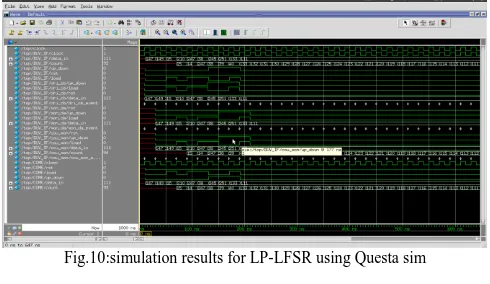
Fig.10:simulation results for LP-LFSR using Questa sim
Fig.11: code coverage report for 64-bit LP-LFSR
6.5 UVM Results
6.5.1 Code Coverage Report
The factory method is a classic software design pattern that is used to create generic code, deferring to run time the exact specification of the object that will be created. In functional verification, introducing class variations is frequently needed. For example, in many tests you might want to derive from the generic data item definition and add more constraints or fields to it; or you might want to use the new derived class in the entire environment or only in a single interface; or perhaps you must modify the way data is sent to the DUT by deriving a new driver. The factory allows you to substitute the verification component without having to provide a derived version of the parent component as well.
Fig.12: UVM Code coverage report 64-bit LFSR
Fig.13: UVM Functional coverage report
The put/get communication as described above allows verification components to be created that model the ―operational‖ behavior of a system. Each component is responsible for communicating through its TLM interface(s) with other components in the system in order to stimulate activity in the DUT and/or respond its behavior. In any reasonably complex verification environment, however, particularly where randomization is applied, a collected transaction should be distributed to the rest of the environment for end-to-end checking (scoreboard), or additional coverage collection
.
As the complexity of VLSI circuits constantly increases, there is a need of a built-in self-test (BIST) to be used. Built-in self-test enables the chip to test itself and to evaluate the circuit’s response. There have been proposed many BIST equipment design methods. In most of the state-of-the-art methods some kind of a pseudorandom pattern generator (PRPG) is used to produce vectors to test the circuit. These vectors are applied to the circuit either as they are, or the vectors are modified by some additional circuitry in order to obtain better functional coverage.
7. Conclusion
8. Future Work
SOC designs are making a rapid shift from mostly digital to mixed signal including millions of user defined logic gates and dozens of IP (Core as well as I/O based). IC Verification and Test strategy needs to include advanced controllers and pattern generators for testing digital as well as analog components of the chip. Pattern generation inside the chip is well known to cause increase in the power consumption of the IC during the manufacturing test. New design and test techniques need to be investigated to keep this increase in the power consumption by the chip as minimum as possible. The availability of advanced manufacturing process rules in the design/verification libraries and tool flow methodologies is mandating the IC front-end designers to verify the manufacturability of the chip much in advance in the design process . Therefore development of the new SOC DFT techniques needs to be compliant with the advanced DFM rules
References
[1] A. S. Abu-Issa and S. F. Quigley, ―Bit-swapping LFSR for low-power BIST,‖ Electron. Lett., vol. 44, no. 6, pp. 401–402, Mar.2013. [2] [K2] IEEE Std. 1364-1995, IEEE Standard Hardware Description Language Based on the Verilog¨ HardwareDescription Language 1995. ISBN 0-7381-3065-6. IEEE Product No. WE94418-TBR.
[3] A. Sagahyroon, G. Lakkaraju and M. karunaratne, "A Functional Verification Environment,", Circuits and Systems Symposium. 48th Midwest, 108-111 Vol.1, 2014
[4] A. Jas, C. V. Krishna, and N. A. Touba, ―Hybrid BISTbased on weighted pseudo-random testing: A new test resource partitioning scheme,‖
in Proc. 19th IEEE Proc. VLSI Test Symp. (VTS), 2001, pp. 2–8.
[5] A. Jas, C. V. Krishna, and N. A. Touba, ―Weighted pseudorandom hybrid BIST,‖ IEEE Trans. Very Large Scale Integr. (VLSI) Syst., vol. 12, no. 12, pp. 1277–1283, Dec. 2004.
[6] R. Kapur, S. Mitra, and T. W. Williams, ―Historical perspective on scan compression,‖ IEEE Design Test, vol. 25, no. 2, pp. 114–120, Mar./Apr. 2008.
[7] B. Koenemann, ―LFSR-coded test patterns for scan designs,‖ in Proc.Eur. Test Conf. (ETC), 1991, pp. 237–242.
[8] Y. Kim, M.-H. Yang, Y. Lee, and S. Kang, ―A new low power test pattern generator using a transition monitoring window based on BIST architecture,‖ in Proc. Asian Test Symp. (ATS), Dec. 2005, pp. 230–235.
[9] C. V. Krishna and N. A. Touba, ―Reducing test data volume using LFSR reseeding with seed compression,‖ in Proc. Int. Test Conf. (ITC), 2002, pp. 321–330.
[10] C. V. Krishna and N. A. Touba, ―Hybrid BIST using an incrementally guided LFSR,‖ in Proc. 18th IEEE Int. Symp. Defect Fault
Tolerance(DFT) VLSI Syst., Nov. 2003, pp. 217–224
[11] IEEE IEEE Standard for SystemVerilog — Unifi ed Hardware Design, Specifi cation, and Verifi cation Language . New York: IEEE 2009 (a.k.a. SystemVerilog Language Reference Manual,or LRM.)
[12] IEEE Standard Verilog Hardware Design, Description Language . New York: IEEE 2001 Rich, Dave Are SystemVerilog Program Blocks Needed?
Acknowledgements
I am great full to Ms. M Chithra M.Tech who is helping and for providing guidelines and encouragement to me and I also thankful to Mr.K.Lokesh Krishna (Ph.D),Dr.C.Chandrashekar (H.O.D) for motivated and encouraged to fulfill this project.
AUTHORS
Kannisetty Reddi Prasad Received B.Tech degree In electronics and communication engineering from Jawaharlal Nehru technological university in 2013,anathapur,A.P,INDIA, and the doing M.Tech degree (SVCET) in electronics and communication engineering (VLSI Design) from Jawaharlal Nehru technological university in 2015,ananthapur,A.P,INDIA