Miniaturized Microstrip Patch Antenna with Defected
Ground Structure
Hanae Elftouh1, *, Naima A. Touhami1, Mohamed Aghoutane1, Safae El Amrani1, Antonio Tazon2, and Mohamed Boussouis1
Abstract—The aim of this work is to miniaturize a microstrip patch antenna resonating at 3 GHz. For this purpose, defected ground structure (DGS) has been employed to shift the resonance frequency of an initial microstrip antenna from 5.7 GHz to 3 GHz by disturbing the antenna’s current distribution. The proposed DGS is incorporated in the ground plane under the patch antenna to improve its performances. Finally, a miniaturization up to 50%, with respect to the conventional microstrip antenna, is successfully accomplished. A prototype of the antenna was fabricated with the FR4 substrate and tested. The measurements results were in good agreement with simulation results.
1. INTRODUCTION
Microstrip patch antennas have been a topic of intense investigation over the last two decades, due to their several advantages and better prospects [1]. Among these advantages we distinguish for instance: lighter weight, lower cost and smaller dimensions. Moreover, microstrip patch antennas can be easily designed to operate in dual-band and multi-band applications, for dual or circular polarization [2]. Thus, they are widely used in many practical applications such as medical applications, satellites and military systems [3].
With the rapid development in wireless communications, much effort has been devoted to reduce the size of microstrip antennas. In this way, several methods have been proposed recently [4], such as using a dielectric substrate of high permittivity [5], Defected Microstrip Structure (DMS) [6], Defected Ground Structure (DGS) at the ground plane [7] or a combination of them.
Mainly DGS is a periodic or non-periodic cascaded defect configuration etched in the ground plane of a planar transmission line. The defect geometry is easy to implement and does not need a large area. These features enable such structures to acquire a great relevance in microwave circuit design [8]. In particular, DGS is employed to design microstrip antennas for different applications, as for instance, cross polarization, mutual coupling reduction in antenna arrays and harmonic suppression. Moreover, DGS has been widely used in the development of miniaturized antennas [9].
When DGS is introduced in a microstrip antenna, the defect geometry etched in the ground plane disturbs its current distribution [10, 11]. This disturbance affects the transmission line characteristics, such as the line capacitance and inductance. In other words, introducing DGS in a microstrip antenna can result in an increase of the effective capacitance and inductance [12] which influences the input impedance and current flow of the antenna [13, 14] and thus reducing its size with respect to a given resonance frequency.
In this paper, we use DGS to design a miniaturized microstrip antenna as compared with a conventional one, resonating at 3 GHz [15]. Initially the proposed antenna resonates at 5.7 GHz, and then DGS is employed to shift the resonance frequency to 3 GHz. Finally, a comparison between our DGS microstrip antenna and the conventional one, at 3 GHz, is carried out.
Received 23 September 2014, Accepted 13 November 2014, Scheduled 18 November 2014
* Corresponding author: Hanae Elftouh ([email protected]).
Figure 1. Top view of our patch antenna resonating at 5.7 GHz, (A= 13 mm, B = 0.2 mm, C = 6.6 mm, D = 2 mm, E = 0.3 mm, F =
2 mm, G = 2 mm, H = 3 mm, I = 3 mm and
J = 12 mm).
Figure 2. Simulated return loss of the patch antenna resonating at 5.7 GHz.
The simulated return loss obtained for this antenna is shown in Fig. 2. We can see that the adaptation is better than 10 dB in a frequency band of about 200 MHz and the resonance frequency is around 5.7 GHz.
3. DEFECTED GROUND STRUCTURE (DGS)
Recently, there has been an increasing interest in the study of microstrip lines with various periodic structures that prohibit wave propagation in certain frequency bands, including photonic band gap (PBG), electromagnetic band gap (EBG) and defected ground structures (DGSs) [16]. Fig. 3 shows
(a) (b) (c) (d) (e)
(f) (g) (h) (i) (j)
Figure 4. Equivalent circuit of DGS.
some of the DGS geometries used, which may be simple or relatively more complicated.
In general, the equivalent circuit of a DGS consists of a parallel tuned circuit in series with the transmission line to which it is coupled [17], as shown in Fig. 4.
The varieties of attached area shapes have the same role and the same characteristics of miniaturization of size, stop band, slow wave effect and high impedance [12–14]. And also they all have the same equivalent circuit. However, we change the kind of DGS only to improve the circuit performance of each antenna.
In our model, radiation and surface wave losses were taken into consideration by including the parallel resistance R in the equivalent circuit.
The equivalent admittance of the parallel resonance is given by Equation (1):
Y = 1 R +j2π
Cf− 1
4π2Lf
(1)
Since Z = 1/Y, then the equivalent impedance is given by
Z = 1/1 R +j2π
Cf− 1
4π2Lf
(2)
In order to compute the equivalent circuit parameters (R, L, and C), we use the following expressions [18]:
S21 =
1
1 +1 2ZZ
−1 0
(3)
S21 =
2Z0
2Z0+
1 R +j2π
Cf− 1
4π2Lf
−1 (4)
Supposing thatRZ0, we obtain: S21=
2Z0
2Z0+
j2π
Cf− 1
4π2Lf
−1 (5)
At −3 dB corresponding to the cutoff frequency fc we have:
|S21|= 2Z0
4Z2
0 +
ωc
Cω2 0−ω2c
2 =
1 √
2 (6)
S21|ω=ω0 = 2Z0
2Z0+Ze
= 2Z0
2Z0+R
(9)
Then,
R =2Z0
1−S21|ω=ω0
S21|ω=ω0
(10)
4. MICROSTRIP PATCH ANTENNA WITH DGS
We introduce DGS in order to shift the resonance frequency of the microstrip antenna previously presented in Fig. 1. First we introduce one cell of the selected DGS geometry and we study its effect on the antenna properties, specially the resonance frequency. Then we introduce a second cell of DGS and do the same study. Both of these simulations have been carried out by CST Microwave Studio.
4.1. With One Cell of DGS
One cell of the selected DGS geometry is etched on the metallic ground plane of our antenna as shown in Fig. 5.
In absence of DGS, we have seen in Section 2 that the resonance frequency of our microstrip patch antenna is at 5.7 GHz. Now with one cell DGS introduced, the simulation result obtained for the return loss is shown in Fig. 6. We can see that the resonance frequency has been significantly influenced by the DGS, namely, it has been brought to about 3.38 GHz.
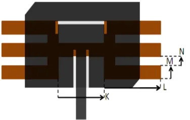
Figure 5. Microstrip patch antenna with one cell DGS (K = 11.5 mm,L= 4 mm,M = 0.7 mm and N = 0.5 mm).
Figure 6. Simulation of return loss for the antenna with one cell of DGS.
4.2. With Two Cells of DGS
Figure 7. Microstrip antenna with two cells of DGS.
Figure 8. Simulation of return loss for the antenna with two cells of DGS.
With two DGS of cells, the return loss simulation result presented in Fig. 8 shows that the resonance frequency has been shifted to around 3 GHz.
Thus, we can say that we have obtained very acceptable result with simulation. Namely, we have designed a microstrip patch antenna with DGS resonating at 3 GHz. Next we present our antenna fabrication and compare simulation with measurement results.
5. FABRICATION AND MEASUREMENT
We have fabricated a prototype of our microstrip patch antenna for each case: one cell and two cells of DGS. We have used an FR4 substrate with relative dielectric constant 4.3 and thickness 1.58 mm. Fig. 9 shows the size of the fabricated DGS microstrip antenna that operates at 3.38 GHz with one cell
(a) (b) (c)
Figure 9. Prototype of DGS microstrip antenna, (a) top view, (b) bottom view with one cell of DGS, (c) bottom view with two cells of DGS.
2 3 4 5 6
x 10 9
Frequency [Hz] Measurement Simulation 0 -10 -20 -30 -40 -50 -60 | S
(1, 1)| [dB]
Figure 10. Measurement and simulation results for the antenna with one cell of DGS (resonating at 3.38 GHz).
2 3 4 5 6
x 10 9
Frequency [Hz] Measurement Simulation 0 -10 -20 -30 -40 -50 -60 | S
(1, 1)| [dB]
WITH DGS AT 3 GHz
6.1. Size Comparison
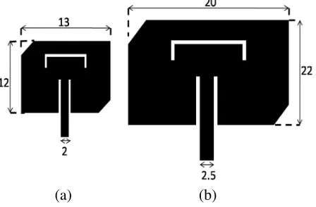
Figure 12 shows a size comparison between a conventional microstrip antenna and the antenna that we have previously designed using two cells of DGS, and both resonating at 3 GHz. We can see that employing a defected ground plane beneath the microstrip patch antenna allows us to reduce the conventional surface up to 50%.
(a) (b)
Figure 12. Top view dimensions (mm) for the 3 GHz antennas, (a) antenna with DGS, (b) conventional antenna.
Figure 13. Radiation pattern for the DGS antenna.
6.2. Radiation Pattern
The radiation patterns presented in Figs. 13 and 14 are obtained for our DGS microstrip antenna and for a conventional microstrip antenna at 3 GHz, respectively. In these figures we can see that the simulated gain for the DGS antenna is 2.14 dBi as for the conventional antenna the simulated gain is 4.41 dBi.
With DGS in the ground plane, the antenna will radiate on both sides of the ground plane due to the aperture efficiency resulting in a high back radiation level which explain the gain reduce about 2 dB. This gain decrease is explained by the increase of lateral and longitudinal radiations due to the propagation of surface waves. Namely, these radiations adversely affect the main lobe power, and therefore a reduction of the gain is produced (see Figs. 13 and 14). In fact, one of the problems in microstrip antenna applications is to reduce the size while keeping good performance.
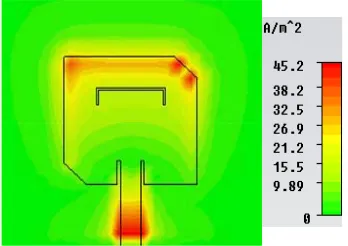
6.3. Current Distribution
To further examine the excitation mechanism, average surface current distributions obtained from CST simulation on both patch and ground plane for optimized antenna were studied. Figs. 15 and 16, show the current distribution of patch antenna without and with DGS respectively at 3 GHz. In conventional antenna, a large surface current was observed over the coins of the patch and along the microstrip line (Fig. 15). However, the current was more concentrated along the DGS on the ground plane of the patch antenna (Fig. 16). The defects on ground structure disturbs the current distribution, resulting in a controlled excitation and propagation of the electromagnetic waves via the substrate layer and change the resonance peak.
Figure 15. The current distribution of conventional antenna at 3 GHz.
(a)
(b)
Cantabria.
REFERENCES
1. Howell, J. Q., “Microstrip antennas,” Dig. Int. Symp. Antennas Propagat. Soc., 177–180, Williamsburg, VA, Dec. 1972.
2. Liu, J., W.-Y. Yin, and S. He, “A new defected ground structure and its application for miniaturized switchable antenna,” Progress In Electromagnetic Research, Vol. 107, 115–128, 2010.
3. Arya, A. K., A. Patnaik, and M. V. Kartikeyan, “Gain enhancement of micro-strip patch antenna using dumbbell shaped defected ground structure,” International Journal of Scientific Research Engineering &Technology (IJSRET), Vol. 2, No. 4, 184–188, Jul. 2013.
4. Nashaat, D., H. A. Elsade, E. Abdallah, H. Elhenawy, and M. F. Iskandar, “Multiband and miniaturized inset feed microstrip patch antenna using multiple spiral-shaped defect ground structure (DGS),” IEEE Antennas and Propagation Society International Symposium, 2009, APSURSI’09, 1–4, Jun. 1–5, 2009.
5. Lo, T. K. and Y. Hwang, “Microstrip antennas of very high permittivity for personal communications,”1997 Asia Pacific Microwave Conference, 253–256, 1997.
6. Tirado-Mendez, J. A., M. A. Peyrot-Solis, H. Jardon-Aguilar, E. A. Andrade-Gonzalez, and M. Reyes-Ayala, “Applications of novel defected microstrip structure (DMS) in planar passive circuits,” Proceedings of the 10th WSEAS International Conference on CIRCUITS, 336–369, Vouliagmeni, Athens, Greece, Jul. 10–12, 2006.
7. Chakraborty, M., B. Rana, P. P. Sarkar, and A. Das, “Size reduction of microstrip antenna with slots and defected ground structure,” International Journal of Electronics Engineering, Vol. 4, No. 1, 61–64, 2012.
8. Elsheakh, D. M., H. A. Elsadek, E. A.-F. Abdallah, H. M. Elhenawy, and M. F. Iskander, “Miniaturized and multiband operations of inset feed microstrip patch antenna by using novel shape of defected ground structure (DGS) in wireless applications,”PIERS Proceeding, 1082–1086, Moscow, Russia, Aug. 18–21, 2009.
9. Kim, H. M. and B. Lee, “Bandgap and slow fast-wave characteristics of defected ground structures (DGSs) including left-handed features,” IEEE Trans. Microwave Theory Techn., Vol. 54, No. 7, 3113–3120, 2006.
10. Arya, A. K., M. V. Kartikeyan, and A. Patnaik, “Efficiency enhancement of microstrip patch antennas with defected ground structure,”Proc. IEEE Recent Advanced in Microwave Theory and Applications (MICROWAVE-08), 729–731, Nov. 2008.
11. Zulkifli, F. Y., E. T. Rahardjo, and D. Hartanto, “Mutual coupling reduction using dumbbell defected ground structure for multiband microstrip antenna array,” Progress In Electromagnetics Research Letters, Vol. 13, 29–40, 2010.
12. Fan, M., R. Hu, Z. H. Feng, X. X. Zhang, and Q. Hao, “Advance in 2D-EBG structures research,”
The Journal of Infrared and Millimeter Waves, Vol. 22, No. 2, 2003.
14. Kapoor, S. and D. Parkash, “Miniaturized triple band microstrip patch antenna with defected ground structure for wireless communication applications,” International Journal of Computer Applications, Vol. 57, No. 7, ISSN: 0975-8887, Nov. 2012.
15. Pozar, D. M., “Microstrip antennas,” Proceedings of the IEEE, Vol. 80, No. 1, 79–91, Jan. 1992. 16. Rahman, M. and M. A. Stuchly, “Transmission line-periodic circuit representation of planar
microwave photonic bandgap structures,” Microw. Opt. Technol. Lett., Vol. 30, 15–19, Jul. 2001. 17. Park, J. S., J. H. Kim, J. H. Lee, S. H. Kim, and S. H. Myung, “A novel equivalent circuit
and modeling method for defected ground structure and its application to optimization of a DGS lowpass filter,” IEEE MTT-S Int. Dig., 417–420, 2002.